#RF PCB Design
Explore tagged Tumblr posts
Visit Tumblr Blog
Explore Tumblr blogs with no restrictions, modern design and the best experience.
Last Seen Tumblr Blogs


Fun Fact
Tumblr Inc. has $15.1M in annual revenue.
Text
Navigating the Future of Electronics with Rigid-Flex and Taconic PCB Manufacturers
Today’s Printed Circuit Boards (PCBs) are much more flexible and advanced than the first rigid versions. Compact devices with great capabilities and multiple features have earned popularity in the electronics industry, leading to the rise of Rigid-Flex PCBs and Taconic PCBs. The use of these technologies enables unique designs, improves how long the device works, and maintains good electricity flow. Rigid-flex PCB Manufacturers can move and also keep their form, similar to how rigid boards function. They particularly shine in high-speed or RF and microwave applications. Dependable and effective products rely greatly on what electronics do.
Rigid-Flex PCBs: Hybrid Structure with High Functionality
Rigid-Flex PCBs take attributes from both stiff and flexible PCBs and merge them into one board. As a result, rigid and flexible boards no longer need connectors and cables, letting us make assemblies that are lighter and more space-saving. You can find these boards in smartphones, medical devices used on patients, military systems and aerospace devices. They are suited for use in places that require resistance to vibration and bending due to machines. In manufacturing, various layers are made and bonded together using very accurate methods. Therefore, it is only experienced manufacturing companies that can keep products of constant quality and performance.
Key Advantages of Rigid-Flex PCB Manufacturers
Important benefits of using well-known Rigid-flex PCB Manufacturers are their excellent design aid and advanced methodologies. They depend on laser direct imaging for precise work and optical inspection that finds problems in the early stage. Tests using temperature fluctuation and electrical overload guarantee that the product will function in any extreme condition. Manufacturers typically boost efficiency by assisting with design changes that lower the number of components and simplify assembly. In addition, they guarantee that flexible circuit boards meet all IPC standards for quality. Because they are involved in developing products and moving them into mass production, they help make the process more efficient.
Taconic PCBs: High-Frequency Performance Excellence
Taconic PCB Manufacturers are produced from proprietary PTFE-based laminates designed by Taconic with low dielectric loss and thermal stability. These boards are the preferred option for RF, microwave, and high-speed digital designs. They are most prevalent in satellite communications, radar systems, 5G base stations, and aerospace communication modules. Taconic laminates have low signal attenuation and superior dimensional stability. They exhibit moisture resistance as well as heat tolerance, which makes them dependable in extreme working environments. Production using these laminates demands proficiency in drilling, plating, and multilayer bonding because of their special properties.
What to Expect from a Taconic PCB Manufacturers
The best Taconic PCB Manufacturers must possess extensive experience in working with high-frequency laminate material. It involves strict impedance control, surface preparation, and low-loss transmission line engineering. Cleanroom facilities, specially designed PTFE-compatible equipment, and precise lamination procedures are necessary for high-quality output. The producers may perform RF testing and thermal profiling to ensure circuit integrity. They also guide customers on stack-up selection as well as PCB layout according to end-use frequency requirements. By maintaining compliance with IPC and MIL-spec specifications, these companies ensure the critical applications' performance and safety.
Comparing Rigid-Flex and Taconic PCBs
Although both are sophisticated PCBs, Rigid-Flex and Taconic PCBs are for different technical applications. Rigid-Flex is prized for mechanical flexibility, whereas Taconic leads for signal transmission at high speeds. Rigid-Flex boards simplify systems and minimize space utilization in cramped enclosures, while Taconic boards maintain signal purity in communication networks. The components and manufacturing methods are quite different, as are the final-use applications. The two are chosen based on physical space, frequency range, and exposure to the environment. Designers will often talk to both varieties of manufacturers to match their circuit requirements with the appropriate solution.
Conclusion
As innovation speeds up in electronics, the need for Rigid-flex PCB Manufacturers and Taconic PCBs keeps increasing. Such technologies facilitate the development of lighter, faster, and more efficient devices across industries. With increasingly sophisticated design challenges, collaborating with an experienced manufacturer is crucial. BS Interconn Hong Kong Co., LIMITED differentiates itself by providing quality-oriented, customer-centric PCB manufacturing services. Whether you're creating a next-generation medical wearable or a state-of-the-art RF device, selecting a reliable Rigid-Flex or Taconic PCB producer guarantees that your product will outperform and outlast the competition.
#Rigid-flex PCB Manufacturers#Taconic PCB Manufacturers#flexible circuit boards#high-frequency PCB#RF PCB solutions#microwave PCBs#PTFE laminates#hybrid PCB design#aerospace PCB#medical device PCBs#5G PCB manufacturer#signal integrity PCB#low dielectric PCB#high-speed PCB#multilayer PCB assembly#IPC compliant PCBs#MIL-spec PCBs#advanced PCB manufacturing#Taconic laminate PCB#Rigid-Flex technology
1 note
·
View note
Text
Best Partner for Wireless Modules: A Comprehensive Antenna Selection Guide
n the field of wireless communication, antenna selection is crucial. It not only affects the coverage range and transmission quality of signals but also directly relates to the overall performance of the system. Among various wireless modules, finding the right antenna can maximize their potential, ensuring stable and efficient data transmission.
When designing wireless transceiver devices for RF systems, antenna design and selection are essential components. A high-quality antenna system can ensure optimal communication distances. Typically, the size of antennas of the same type is proportional to the wavelength of the RF signal; as signal strength increases, the number of required antennas also grows.
Antennae can be categorized as internal or external based on their installation location. Internal antennas are installed within the device, while external antennas are mounted outside.
In situations where space is limited or there are multiple frequency bands, antenna design becomes more complex. External antennas are usually standard products, allowing users to simply select the required frequency band without needing additional tuning, making them convenient and easy to use.
What are the main types of antennas?
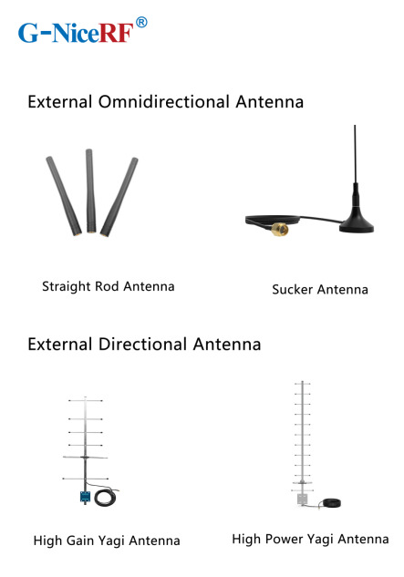
External Antennas: These antennas can be classified into omnidirectional antennas and directional antennas based on the radiation pattern.
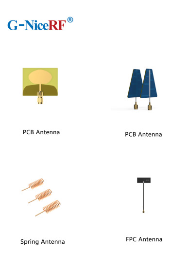
Internal Antennas: These antennas refer to antennas that can be placed inside devices.
Omnidirectional Antennas: These antennas radiate signals uniformly in the horizontal plane, making them suitable for applications that require 360-degree coverage, such as home Wi-Fi routers and mobile devices.
Directional Antennas: These antennas have a high emission and reception strength in one or more specific directions, while the strength is minimal or zero in others. Directional antennas are primarily used to enhance signal strength and improve interference resistance.
PCB Antennas: These antennas are directly printed on the circuit board and are suitable for devices with limited space, commonly used in small wireless modules and IoT devices.
FPC Antennas: FPC antennas are flexible printed circuit antennas that are lightweight, efficient, and easy to integrate.
Concealed Antennas: Designed for aesthetic purposes, concealed antennas can be hidden within devices or disguised as other objects, making them suitable for applications where appearance is important without compromising signal quality.
Antenna Selection Guide
When selecting the appropriate antenna for a communication module, it's essential to first determine whether to use an internal or external antenna based on the module's structure.
External Antennas: These antennas offer high gain, are less affected by the environment, and can save development time, but they may take up space and impact the product's aesthetics.
Internal Antennas: These have relatively high gain and are installed within the device, maintaining a clean and appealing exterior.
Sucker Antennas: These provide high gain and are easy to install and secure.
Copper Rod Sucker Antennas: Made from large-diameter pure copper radiators, these are highly efficient with a wide bandwidth.
Rubber Rod Antennas: Offer moderate gain at a low cost.
Fiberglass Antennas: Suitable for harsh environments and ideal for long-distance signal

External Directional Antennas
Typically used in environments with long communication distances, small signal coverage areas, and high target density.
Panel Antennas��have high efficiency, are compact, and easy to install, while considering the impact of gain and radiation area Yagi Antennas offer very high gain, are slightly larger, and have strong directionality, making them suitable for long-distance signal transmission; however, attention must be paid to the antenna's orientation during use
Internal Antenna Selection
Most internal antennas are affected by environmental factors and may require custom design or impedance matching
Spring Antennas are cost-effective but have low gain and narrow bandwidth, often requiring tuning for good matching when installed Ceramic Patch Antennas occupy minimal space and perform well, but have a narrow bandwidth
For details, please click:https://www.nicerf.com/products/ Or click:https://nicerf.en.alibaba.com/productlist.html?spm=a2700.shop_index.88.4.1fec2b006JKUsd For consultation, please contact NiceRF (Email: [email protected]).
2 notes
·
View notes
Text
At work they seem to think I'm an electrical engineer. I'm just. Just so baffled by this. If there's one thing I'm not, surely it's that.
Like, ok, the mechanical engineers think I'm a mechanical engineer, and that's fine. The bosses think everyone is a mechanical engineer, or can be, given half a chance. They think the actual mechanical engineers--the ones with masters degrees in mechanical engineering--are simply the most experienced, but that anyone else could do their job slightly worse but basically successfully. But the mechanical engineers treat me like I'm one of them in a way they don't with other physicists, trust me with tools that they wouldn't trust others with, one of them even gave me admin privileges to some equipment that they won't give my supervisor admin privileges to. Apparently they thought I was going to be working 3/4 time as a physicist and 1/4 time as a laser engineer when I was hired; my previous employer killed that possibility (the one real concession he got with his threatened lawsuit was that I'm not allowed to work on the insides of any lasers for two years) but that's still how they think of me, as basically one of them. But that's just the mechanical engineers who see me that way.
When I applied I said I had mechanical engineering experience and software experience. I hate software, but you've gotta put that in your resume, if you can do it even a little bit. My supervisor remembered that and took it seriously, and I do actually do some software engineering when I have to, but the bosses mainly don't want me working on software.
But somehow the bosses think I'm an electrical engineer, instead. That I should be a major bridge between the electrical engineering department and physics. That that's my rare expertise rather than (in my opinion) my most embarrassing incompetence, the one thing I try to avoid having come up in job interviews because I can't find a positive spin for it.
I mean. It's kind of good, because the company president sees himself as being an electrical engineer as well as a physicist. So he's like, oh, we have this extra competency in common! And it's also kind of good that the skillset that I'm the least secure about, other people have convinced themselves that I'm good at--although I think that's partly because they haven't really asked that much of me, and partly because I know a bit about rf/mw. But, like, I can barely design an inverting amplifier or a low pass filter and then put it together with large components from a kit (although it'll look reasonably nice if I do, because my soldering is decent). And I've only actually laid out a PCB for manufacturing exactly once in my entire life. But it's, idk, weird. I rarely get anything that looks like imposture syndrome, but I can feel it creeping in a little bit here. (Except, of course, it's justified.)
#you may wonder then: if they see me as an electrical engineer surely that implies they're assigning me electrical engineering projects#so how do I get those done in such a way that the bosses are pleased with me?#because surely they're pleased with me if they've--after 10 months of employment--convinced themselves that I can do this?#well: I delegate these tasks to one of the actual electrical engineers rather than doing them myself#(which is the same thing my supervisor does--but unlike the bosses I don't think my supervisor thinks I'm an electrical engineer)#(then again the bosses think my supervisor is this superstar who's excellent at literally everything#so I guess this MUST be a winning strategy)#the engineers are considered more or less support staff to the physicists so the electrical engineer that I'm delegating to#sees picking up assignments like this from physicists who don't want to do it themselves as a core part of his job#rather than feeling that I'm taking time away from his own projects or something#I don't know how the bosses see it though if they think this shows MY competence as an electrical engineer
4 notes
·
View notes
Text
Top 15 PCB Board Manufacturers in USA

When it comes to building reliable electronics, choosing the right PCB board manufacturer in USA is critical. Whether you’re a startup, engineer, OEM, or tech company, having a dependable partner for printed circuit board fabrication and assembly ensures faster production, fewer errors, and better results.
In this blog, we list the Top 15 PCB board manufacturers in the USA known for high-quality PCB fabrication, assembly, and fast delivery. These companies are widely searched and trusted across various industries — from medical to aerospace, IoT, automotive, and industrial applications.
1. PCB Power
PCB Power is one of the most trusted names among PCB board manufacturers USA. With over two decades of industry experience, PCB Power offers quick-turn PCB fabrication, full turnkey assembly, and components sourcing — all under one roof.
As a USA-based PCB company, they focus on delivering high-quality single, double, and multilayer PCBs with fast turnaround and competitive pricing. Whether you’re building prototypes or mass production, PCB Power’s online ordering system makes it easy to get instant quotes, track orders, and communicate with real engineers.
Key Features:
US-based production for fast and reliable delivery
ISO-certified processes for superior quality
Advanced manufacturing for high-density, multilayer PCBs
Turnkey assembly and BOM handling
Expert support for startups, engineers, and OEMs
If you’re looking for a complete PCB manufacturing solution in the USA, PCB Power should be your first stop.
2. Advanced Circuits
Advanced Circuits is one of the largest and oldest PCB manufacturers in the United States. Known for high-quality prototypes and low-to-medium volume production, they serve industries like aerospace, defense, and telecom.
They offer same-day and next-day shipping options and have their own in-house manufacturing for consistent quality.
3. Sierra Circuits
Sierra Circuits is a full-service PCB company specializing in quick-turn fabrication and assembly. They’re well-known for their high-performance HDI PCBs, rigid-flex boards, and support for complex designs. Sierra Circuits is ideal for companies looking for technical precision and tight tolerances.
4. Sunstone Circuits
Sunstone Circuits has built a reputation for delivering reliable prototype PCBs and small-batch orders. Their online design tools and instant quote system are ideal for hobbyists, startups, and small engineering teams. Their US-based manufacturing ensures high quality and fast shipping.
5. Bay Area Circuits
Located in California, Bay Area Circuits serves the Silicon Valley tech community with rapid prototyping, fabrication, and assembly services. They are experts in small-run production and serve various industries including medical, aerospace, and communications.
6. Rush PCB Inc.
Rush PCB Inc. offers full turnkey PCB services, including design, manufacturing, and assembly. They specialize in multilayer, flex, and rigid-flex PCBs with quick-turn options. Their experienced team supports everything from prototypes to volume production.
7. Custom Circuit Boards
Based in Arizona, Custom Circuit Boards provides high-quality PCBs for engineers and hardware startups. They focus on fast production and specialize in multilayer boards, thick copper PCBs, and RF designs.
8. Imagineering Inc.
Imagineering Inc. offers both PCB fabrication and assembly with ISO 9001 and AS9100 certifications. They serve demanding industries like medical and aerospace and are known for excellent quality and fast lead times.
9. Epec Engineered Technologies
Epec is a full-service provider offering custom PCB manufacturing, flexible circuits, and battery packs. With decades of experience, they provide engineered solutions for complex applications and tight deadlines.
10. APCT Inc.
APCT is known for high-speed, high-density interconnect PCBs. They support quick-turn and production-scale manufacturing. Their specialties include aerospace and defense-grade boards with rigorous quality requirements.
11. OnBoard Circuits
OnBoard Circuits offers affordable PCB prototyping, fabrication, and assembly with domestic and offshore capabilities. They are known for great customer support and fast delivery for small to medium volume orders.
12. Millennium Circuits Limited (MCL)
MCL provides reliable PCBs including rigid, flex, and rigid-flex boards. They serve industries like telecom, industrial, and medical, offering fast turnaround times and excellent pricing.
13. TechnoTronix
TechnoTronix offers advanced PCB manufacturing and assembly solutions with a strong focus on precision and fast lead times. They work with both small businesses and large enterprises, offering everything from basic to complex PCB designs.
14. RedBoard Circuits
RedBoard Circuits provides quality PCBs with a focus on customer service and quick delivery. They offer a wide range of PCB types including FR4, aluminum, and Rogers materials.
15. ALLPCB USA
ALLPCB USA offers cost-effective PCB solutions with a quick-turn focus. They provide both prototype and production runs and serve customers looking for affordable yet reliable circuit boards.
Choose the Best PCB Manufacturer for Your Needs
Selecting the right PCB board manufacturer in USA can be the difference between a successful project and costly delays. Whether you need fast prototyping, volume production, or full turnkey PCB assembly, each of these top 15 manufacturers brings something unique to the table.
However, if you’re looking for a complete solution with fast delivery, reliable quality, and competitive pricing — PCB Power is a clear leader. With US-based manufacturing, expert support, and a user-friendly online ordering platform, PCB Power makes your PCB journey seamless from design to delivery.
0 notes
Text
Reliable Metal Clad PCB Suppliers in India: Vaishnavi Electronics at the Forefront of Innovation
As the electronics industry moves toward higher power and thermal efficiency, Metal Clad PCBs (MCPCBs) have become an essential component in modern electronic design. Known for their superior heat dissipation, durability, and performance in high-power applications, MCPCBs are widely used in LED lighting, automotive electronics, power converters, and industrial equipment. In India, Vaishnavi Electronics stands out as one of the most dependable metal clad PCB suppliers, known for its quality manufacturing, technical expertise, and customer-centric approach.
The Strategic Importance of Metal Clad PCBs in High-Power Applications
Metal Clad PCBs, often composed of a thermally conductive dielectric layer sandwiched between a metal base (typically aluminum or copper) and a copper circuit layer, are engineered to manage heat more efficiently than standard PCBs. Their ability to draw heat away from active components ensures longer lifespan, higher reliability, and improved performance in thermally demanding environments.
Unlike traditional PCBs, MCPCBs allow designers to use higher power densities and compact layouts without compromising thermal performance. They are particularly valuable in LED lighting systems, where excessive heat can degrade performance, as well as in power supply units, motor controllers, and RF applications.
As demand for energy-efficient and high-performance devices increases, so does the need for advanced PCB solutions like metal clad boards. This has positioned quality suppliers like Vaishnavi Electronics as critical partners for OEMs and electronics manufacturers across sectors.
Vaishnavi Electronics: Trusted Partner for Custom Metal Clad PCB Solutions
Vaishnavi Electronics, based in India, has earned a reputation as a leading supplier of metal clad PCBs, offering reliable and tailored solutions that meet the specific needs of its clients. The company has invested in advanced manufacturing processes and quality control systems to ensure consistent production of high-performance MCPCBs.
With capabilities to work on various metal substrates—such as aluminum, copper, and steel—Vaishnavi Electronics supports a wide range of applications, from LED modules to power management systems. The company’s expertise extends beyond standard offerings; it provides customized MCPCB solutions, including multi-layer constructions, specific thermal conductivity requirements, and design support for complex layouts.
Vaishnavi’s production process emphasizes durability, thermal stability, and electrical integrity. Every MCPCB undergoes rigorous testing to ensure it meets industry standards for thermal resistance, mechanical strength, and electrical performance. Additionally, their engineering team works closely with clients to optimize board layout for maximum efficiency and reliability.
What sets Vaishnavi Electronics apart is not just its technical know-how but its commitment to customer service. Whether it's rapid prototyping or bulk production, the company delivers on time, offering competitive pricing without compromising on quality.
In conclusion, the growing demand for Metal Clad PCB suppliers across high-power and thermally challenging applications highlights the need for experienced and dependable suppliers. Vaishnavi Electronics continues to lead the way in India’s PCB industry with its advanced capabilities, customized solutions, and unwavering focus on quality. For businesses seeking a trusted partner in metal clad PCB supply, Vaishnavi Electronics offers a strategic advantage through innovation, reliability, and precision manufacturing.
Visit:- https://www.vaishnavielectronics.co.in/metal-clad-pcb.html
0 notes
Text
ASC-i's Advanced RF Test Capabilities: Ensuring Peak Performance for Your RF PCB Designs
As an industry-leading RF PCB manufacturer, ASC-i is dedicated to providing high-performance, high-quality solutions for a wide range of applications, including wireless communication, automotive radar, medical devices, and IoT systems. When it comes to RF PCBs, ensuring the reliability and functionality of the circuits is paramount. With our advanced RF test capabilities, we ensure that every PCB we produce meets the rigorous demands of the RF industry, delivering optimal performance across all environments and conditions.

The Importance of RF Testing for High-Quality PCB Manufacturing
Radio Frequency (RF) signals are critical for modern communication systems, and even the smallest flaw in the design or manufacturing of an RF PCB can lead to signal loss, interference, or even complete failure. This is why thorough RF testing is essential at every stage of PCB production. At ASC-i, we recognize that precise testing ensures the signal integrity, performance, and durability of the final product. Our RF testing services are designed to identify potential issues early, ensuring that your designs perform at their best before they are integrated into end-use products.
As a trusted RF PCB manufacturer, ASC-i provides comprehensive testing solutions that guarantee each RF PCB we create meets the highest industry standards. Whether you're developing high-frequency communication systems or specialized RF devices, we have the expertise and tools to ensure your products meet exacting specifications.
ASC-i’s Advanced RF Test Capabilities
Our RF test capabilities are built to cover every essential aspect of RF performance, ensuring that your RF PCBs operate reliably and efficiently. Our testing process focuses on key parameters such as signal integrity, impedance matching, thermal stability, power handling, and electromagnetic compatibility. Here’s an overview of our comprehensive RF testing services:
S-Parameter Testing: S-parameters, or scattering parameters, measure the reflection and transmission characteristics of RF circuits. By using high-precision network analyzers, ASC-i tests the insertion loss, return loss, and signal integrity of the RF PCB. This allows us to ensure that the board exhibits minimal signal degradation and high performance under real-world conditions.
Impedance Matching Tests: One of the most critical aspects of RF circuit performance is impedance matching. Proper impedance ensures that the signal is transmitted without reflection or loss. We perform detailed impedance testing across PCB traces, vias, and components to ensure that the impedance is optimized, guaranteeing smooth and efficient signal transmission.
RF Power Handling Testing: RF PCBs often need to handle high power levels, especially in demanding applications like wireless communication, radar, and broadcast systems. We test the power-handling capacity of your PCB to ensure that it can withstand high power inputs without compromising performance or causing thermal issues.
Thermal Performance Testing: RF circuits generate heat, and without proper heat management, thermal buildup can lead to degradation in signal quality or even failure of components. ASC-i conducts comprehensive thermal tests to evaluate how effectively the RF PCB dissipates heat and performs under varying temperature conditions.
Environmental and Aging Tests: To simulate the real-world conditions your RF PCB will face over time, we perform aging and environmental tests that assess how the board handles temperature fluctuations, humidity, vibration, and other environmental factors. This ensures that the RF PCB is durable and can withstand long-term use.
Electromagnetic Interference (EMI) Testing: EMI can significantly disrupt the performance of RF circuits. Our EMI testing ensures that your PCB meets electromagnetic compatibility standards, minimizing the risk of interference with nearby components and ensuring that the device operates smoothly in its intended environment.
Custom RF Testing Solutions for Every Need
At ASC-i, we know that each project is unique. Whether you’re designing a wireless communication system, automotive radar unit, or medical RF device, our team of engineers is ready to customize our testing solutions to meet the specific needs of your design. We work closely with you to understand the requirements of your project and develop a tailored testing plan that addresses all relevant performance factors.
By providing tailored testing services, we ensure that your RF PCBs will meet the precise criteria for your application, ensuring flawless performance across different environments and use cases.
Why Choose ASC-i as Your RF PCB Manufacturer?
Expertise and Experience: With years of experience in designing and manufacturing RF PCBs, ASC-i brings invaluable expertise to every project. Our engineers are well-versed in RF design principles and testing methods, allowing us to deliver high-quality, high-performance RF PCBs for a wide range of applications.
State-of-the-Art Testing Equipment: ASC-i uses the latest testing technologies and equipment to ensure the accuracy and precision of our testing processes. Our RF testing labs are equipped with advanced tools such as network analyzers, spectrum analyzers, thermal chambers, and more to ensure that each PCB is tested to the highest standards.
Comprehensive Testing Services: From signal integrity to thermal and environmental testing, ASC-i provides a full spectrum of RF test services. Our rigorous testing process ensures that each PCB performs optimally in its intended application, providing a reliable solution for every project.
Customization: Every RF PCB design has unique needs. ASC-i offers customized RF testing solutions that can be tailored to meet the specific parameters of your design. We take a collaborative approach to understand the requirements of your project and offer flexible testing services to address your needs.
Quality Assurance: At ASC-i, we prioritize quality in every stage of the manufacturing and testing process. Our robust testing procedures help identify and address any potential issues early, ensuring that your RF PCB meets the highest standards of reliability, durability, and performance.
Timely and Cost-Effective Solutions: We understand the importance of meeting deadlines in the fast-paced world of electronics. ASC-i offers quick turnaround times without compromising quality, allowing you to meet your project timelines while keeping costs under control. Our streamlined processes ensure that you receive competitive pricing for top-tier testing and manufacturing services.
Conclusion
ASC-i is your trusted partner for RF PCB manufacturing and testing services. Our advanced RF test capabilities, coupled with our expertise in RF design and production, allow us to deliver high-quality RF PCBs that perform reliably in the most demanding applications. Whether you’re developing a new wireless communication device, automotive radar system, or medical equipment, ASC-i’s comprehensive RF testing ensures that your PCB will meet the highest standards of performance, reliability, and durability.
Partner with ASC-i today and experience the difference our advanced RF testing capabilities can make for your RF PCB designs. We’re here to help you achieve success by delivering top-quality, high-performance solutions that meet the challenges of today’s technology-driven world. Contact us to learn more about our RF PCB manufacturing and testing services.
0 notes
Text
Why Are Surface Mount Inductors Vital in Modern Electronics? A Complete Guide

Surface mount inductors have emerged as critical components in today’s compact and high-performance electronic devices. As the demand for miniaturization and efficiency continues to grow, these components offer a reliable solution for energy storage, filtering, and signal integrity. Whether you are designing consumer electronics, industrial systems, or automotive applications, understanding the role and advantages of surface mount inductors can significantly enhance your product development process.
What Are Surface Mount Inductors?
Surface mount inductors are passive electronic components designed to store energy in a magnetic field when electrical current flows through them. Unlike traditional through-hole inductors, surface mount variants are mounted directly onto the surface of a printed circuit board (PCB), enabling compact, low-profile, and automated assembly designs. These inductors are widely used for their efficient space utilization and high-frequency performance.
How Do Surface Mount Inductors Work?
The basic working principle of surface mount inductors is grounded in electromagnetic induction. When current passes through the coil inside the inductor, it creates a magnetic field. This field resists changes in the current, providing a filtering or energy storage function depending on the application.
Surface mount inductors are typically manufactured using a ferrite or powdered iron core surrounded by a coiled conductor. The magnetic properties of the core and the number of coil turns determine the inductance value. Their compact design allows them to perform reliably in dense circuit boards.
Where Are Surface Mount Inductors Used?
These inductors are essential in multiple sectors where space-saving components are crucial. Common applications include:
Smartphones, tablets, and laptops
Power supplies and DC-DC converters
Automotive electronic control units (ECUs)
RF and telecommunications systems
Medical and industrial instrumentation
LED lighting systems and IoT modules
Each of these areas requires high-performance signal integrity and energy efficiency, both of which are facilitated by surface mount inductors.
What Are the Key Benefits of Surface Mount Inductors?
Surface mount inductors provide a range of advantages for engineers and product designers. Their integration into compact electronics is particularly valuable in today’s market.
Enable miniaturized circuit design for compact devices
Support high-frequency operations with excellent performance
Reduce production time through automated pick-and-place mounting
Offer low DC resistance (DCR) for higher efficiency
Enhance electromagnetic compatibility (EMC) in sensitive circuits
Provide thermal stability in harsh environments
Available in a wide variety of inductance values and sizes
These benefits make them indispensable in both analog and digital electronic systems.
What Are the Different Types of Surface Mount Inductors?
The choice of surface mount inductor depends on the specific application and performance requirements. Key types include:
Wire-wound inductors: Known for high Q-factor and current handling capabilities, ideal for power applications.
Multilayer inductors: Offer compact size and are suitable for high-frequency filtering.
Thin-film inductors: Deliver precision and low-profile characteristics, often used in RF circuits.
Molded inductors: Provide strong mechanical durability, often used in automotive environments.
Each type has unique characteristics that influence its behavior in a circuit, and selecting the right one depends on factors such as frequency, current rating, and size constraints.
How to Choose the Right Surface Mount Inductor?
Selecting the right surface mount inductor for your application involves considering several important technical parameters:
Inductance (L): Measured in microhenries (µH) or nanohenries (nH), this value defines how much energy the inductor can store.
Current rating: Determines the maximum current the inductor can handle without saturating or overheating.
Saturation current: Indicates the point at which the inductor loses its inductive properties.
DC resistance (DCR): Lower DCR means better efficiency and less power loss.
Frequency range: Ensures compatibility with the intended signal or switching frequency.
Size and footprint: Must match the PCB layout and spatial constraints.
Understanding these parameters helps ensure optimal circuit performance, reliability, and compliance with regulatory standards.
Why Are Surface Mount Inductors Preferred Over Through-Hole Types?
While both surface mount and through-hole inductors serve similar electrical purposes, surface mount options are increasingly preferred in modern electronic assemblies. This shift is driven by:
Smaller package sizes suitable for compact PCBs
Better performance at higher frequencies
Faster, more cost-effective automated manufacturing
Improved thermal performance in high-density applications
Enhanced mechanical stability during vibration or movement
Surface mount technology enables the design of lightweight, efficient, and high-performance devices across various industries.
What Are the Trends in Surface Mount Inductor Technology?
As technology evolves, surface mount inductors continue to improve in performance, durability, and miniaturization. Key developments in this field include:
Use of advanced core materials for higher energy density
Lower EMI solutions to support 5G and wireless technologies
Integration with ICs and other passives for modular designs
Eco-friendly manufacturing with lead-free soldering
High-reliability solutions for automotive and aerospace sectors
These innovations make surface mount inductors a forward-looking solution for next-generation electronic products.
Where to Buy High-Quality Surface Mount Inductors?
Finding trusted suppliers is essential for securing reliable surface mount inductors. It’s important to source components from distributors that provide:
Comprehensive technical datasheets
RoHS-compliant and quality-certified components
Wide inventory of top brands and value options
Global shipping and responsive customer service
Compatibility with high-frequency and power electronics
Buyers and engineers should consider trusted electronic suppliers with extensive product listings and verified sourcing standards.
Conclusion
Surface mount inductors are indispensable building blocks of today’s advanced electronic systems. Their compact form factor, high-frequency capability, and reliable performance make them ideal for power conversion, signal conditioning, and EMI suppression tasks. By understanding how these components work, where they are used, and how to select the right one, engineers can unlock new possibilities in their designs. As innovation accelerates, surface mount inductors continue to play a central role in enabling smarter, smaller, and more efficient electronics.
0 notes
Text
Global WiFi and Bluetooth RF Antenna Market: Growth Drivers, Technological Advancements, and Forecast 2025–2032
MARKET INSIGHTS
The global WiFi Bluetooth Radio Frequency Antenna Market size was valued at US$ 4.86 billion in 2024 and is projected to reach US$ 8.42 billion by 2032, at a CAGR of 8.3% during the forecast period 2025-2032. The U.S. market accounted for 32% of global revenue in 2024, while China is expected to witness the fastest growth with an estimated 9.1% CAGR through 2032.
WiFi Bluetooth Radio Frequency Antennas are critical components that enable wireless communication across multiple frequency bands, including 2.4GHz and 5GHz for WiFi and 2.4GHz ISM band for Bluetooth. These antennas are categorized into internal (PCB, chip, flexible printed circuit) and external (directional, omnidirectional) types, each offering distinct advantages in terms of size, gain, and radiation patterns. Advanced antenna technologies like MIMO (Multiple Input Multiple Output) are increasingly being integrated to enhance data throughput and connection reliability.
The market growth is driven by surging demand for IoT devices, which grew by 18% year-over-year in 2023, and the rapid adoption of 5G networks requiring advanced RF solutions. Automotive applications represent the fastest-growing segment, projected to account for 28% of market share by 2032 due to increasing vehicle connectivity features. Key industry players including TE Connectivity, Molex, and Amphenol collectively held 45% market share in 2024, with recent product launches focusing on miniaturized antennas for wearable devices and automotive-grade solutions.
MARKET DRIVERS
Proliferation of IoT Devices and Connected Technologies to Accelerate Market Growth
The exponential growth of IoT devices across industries is driving unprecedented demand for WiFi Bluetooth radio frequency antennas. With over 40 billion active IoT connections expected by 2025, the need for reliable wireless connectivity solutions has never been higher. These antennas serve as critical components in smart home ecosystems, industrial automation systems, and wearable technologies, enabling seamless data transmission across networks. The automotive sector’s rapid adoption of vehicle-to-everything (V2X) communication technologies further amplifies this demand, with modern vehicles requiring multiple antennas for navigation, entertainment, and safety systems.
Advancements in 5G Infrastructure Deployment to Fuel Antenna Innovation
Global 5G network expansion is creating substantial opportunities for advanced antenna technologies. Current 5G implementations require sophisticated antenna designs capable of supporting higher frequency bands while maintaining efficient power consumption. The transition to millimeter wave (mmWave) frequencies in particular demands innovative antenna solutions that can overcome propagation challenges. Manufacturers are responding with compact, high-performance antennas featuring beamforming capabilities and improved signal-to-noise ratios. For instance, recent development cycles have seen a 35% improvement in antenna efficiency for mmWave applications compared to previous generations.
Increasing Consumer Demand for High-Speed Wireless Connectivity to Drive Adoption
Consumer expectations for uninterrupted, high-bandwidth connectivity continue to shape antenna technology development. The average household now contains more than 10 connected devices, each requiring robust wireless performance. This trend has led antenna manufacturers to focus on multi-band solutions that can simultaneously support WiFi 6/6E, Bluetooth 5.x, and emerging standards. Streaming applications alone account for over 65% of internet traffic during peak hours, creating persistent demand for antennas with superior range and interference mitigation capabilities. Recent product launches demonstrate significant improvements in throughput, with some consumer-grade antennas now supporting concurrent data rates exceeding 3 Gbps.
MARKET RESTRAINTS
Signal Interference and Spectrum Congestion Challenges Impacting Performance
The growing density of wireless devices creates significant challenges for maintaining signal integrity. In urban environments, spectrum congestion has reached critical levels, with some frequency bands exhibiting interference levels that degrade antenna performance by up to 40%. This is particularly problematic for Bluetooth Low Energy (BLE) applications in crowded settings like retail stores or smart offices. Device manufacturers must implement increasingly sophisticated filtering techniques and adaptive algorithms to counteract interference, which adds complexity and cost to antenna systems.
Miniaturization Constraints Limiting Design Options
The relentless push for smaller form factors in consumer electronics presents substantial engineering challenges for antenna designers. As device footprints shrink, antennas must maintain performance while occupying less than half the space they required five years ago. This miniaturization often comes at the expense of radiation efficiency, with some compact antennas experiencing up to 30% reduction in effective range compared to their larger counterparts. The integration of multiple wireless protocols into single-chip solutions further exacerbates these constraints, requiring careful optimization of PCB layout and component placement.
MARKET CHALLENGES
Complex Certification Processes Delaying Time-to-Market
Navigating global regulatory requirements remains a persistent challenge for antenna manufacturers. Each region maintains distinct certification protocols for wireless devices, with testing procedures often taking six months or longer to complete. The introduction of new frequency bands for 5G and WiFi 6E has added further complexity, requiring extensive retesting for compliance with evolving standards. These delays can significantly impact product launch timelines and increase development costs, particularly for small and medium-sized enterprises.
Supply Chain Vulnerabilities Affecting Component Availability
The antenna industry faces ongoing supply chain disruptions affecting critical materials and components. Specialty substrates and high-frequency laminates essential for advanced antenna designs have experienced lead time extensions of up to 12 months in some cases. Semiconductor shortages have also impacted integrated RF front-end modules, creating production bottlenecks. These constraints have compelled manufacturers to redesign products around available components, sometimes compromising performance specifications to maintain shipment schedules.
MARKET OPPORTUNITIES
Emergence of Smart Cities and Infrastructure Creates New Demand Channels
The global smart city initiative represents a substantial growth opportunity for antenna manufacturers. Municipal deployments of IoT sensors, traffic management systems, and public safety networks require robust wireless infrastructure. These applications often necessitate ruggedized antenna solutions capable of withstanding harsh environmental conditions while maintaining reliable connectivity across diverse urban landscapes. Recent pilot programs have demonstrated that smart city networks can reduce operational costs by up to 30% while improving service delivery, indicating strong potential for continued investment in these technologies.
Advancements in Material Science Enabling Next-Generation Antennas
Breakthroughs in metamaterials and flexible electronics are opening new possibilities for antenna design. Researchers have developed composite materials that exhibit negative refraction indexes, allowing for unprecedented control over electromagnetic wave propagation. These innovations support the development of conformal antennas that can be integrated into clothing, flexible displays, and curved surfaces without sacrificing performance. Early prototypes demonstrate 40% wider bandwidth and improved gain characteristics compared to conventional designs, suggesting significant potential for commercialization in coming years.
Integration of AI for Adaptive Antenna Systems Creates Competitive Advantage
The incorporation of machine learning algorithms into antenna control systems represents a transformative opportunity for the industry. Modern adaptive antenna arrays can now employ real-time pattern optimization based on environmental conditions and usage patterns. These intelligent systems demonstrate remarkable improvements in energy efficiency, with some implementations reducing power consumption by up to 60% during low-demand periods. As edge computing capabilities expand, the ability to locally process signal data and optimize radiation parameters will become an increasingly valuable differentiator in competitive markets.
WI-FI BLUETOOTH RADIO FREQUENCY ANTENNA MARKET TRENDS
5G and IoT Expansion Driving Antenna Innovation
The proliferation of 5G networks and IoT devices is significantly accelerating demand for advanced Wi-Fi and Bluetooth RF antennas. With over 1.4 billion 5G connections globally as of recent data, manufacturers are developing compact, high-performance antennas that support wider frequency ranges (2.4GHz-6GHz) and MIMO (Multiple Input Multiple Output) configurations. The automotive sector particularly demonstrates growth, where premium vehicles now incorporate 15+ antennas for connected features. Emerging antenna-on-chip (AoC) and antenna-in-package (AiP) technologies are enabling smaller form factors while maintaining signal integrity in space-constrained applications like wearables and smart home devices.
Other Trends
Miniaturization and Integration Challenges
As consumer electronics shrink, antenna designers face mounting pressure to deliver sub-6mm solutions without sacrificing performance. While chip antennas dominate smartphone applications (85% market penetration in flagship devices), hybrid designs combining ceramic and PCB antennas are gaining traction for industrial IoT applications requiring ruggedness. The trade-off between size and efficiency remains critical – recent tests show compact antennas can experience 15-20% efficiency drops compared to traditional external antennas. Manufacturers are countering this through advanced simulation tools and metamaterial coatings that enhance radiation patterns.
Automotive Connectivity Demand Surge
The automotive sector is emerging as a key growth vertical, with connected car antennas expected to comprise 30% of the market by 2026. Modern vehicle architectures require antennas supporting Wi-Fi 6, Bluetooth 5.2, C-V2X, and satellite communications simultaneously. This complexity drives adoption of multi-band, multi-protocol antenna arrays, particularly for electric vehicles where traditional shark-fin housings interfere with aerodynamics. Recent developments include embedded glass antennas and conformal designs molded into body panels, yielding 40% space savings while maintaining 5dB gain improvements over conventional whip antennas.
WiFi Bluetooth Radio Frequency Antenna Market – Competitive Landscape
Key Industry Players
Innovation and Market Expansion Drive Fierce Competition Among Antenna Manufacturers
The global WiFi Bluetooth Radio Frequency Antenna market is characterized by moderate consolidation, with major players competing alongside emerging manufacturers. Leading companies are focusing on miniaturization, multi-band compatibility, and improved signal efficiency to maintain their competitive edge. The market is witnessing accelerated growth due to increasing demand across automotive, consumer electronics, and IoT applications.
TE Connectivity and Amphenol currently dominate the global antenna market, collectively holding approximately 30% market share in 2024. Their dominance stems from extensive product portfolios spanning internal and external antennas, along with strong distribution networks across North America and Europe. Both companies have recently introduced 5G-compatible antennas, addressing the growing need for high-speed connectivity in smart devices.
Molex and Laird Connectivity are emerging as significant competitors, particularly in the automotive electronics sector. These companies are investing heavily in low-profile antenna designs that can be integrated seamlessly into modern vehicle architectures. Their focus on automotive-grade reliability and extended temperature range performance gives them an advantage in this demanding application segment.
The competitive landscape is further enriched by specialized manufacturers like Taoglas and C&T RF Antennas, who are carving niches in high-performance industrial applications. These companies differentiate themselves through proprietary technologies such as beamforming antennas and advanced impedance matching techniques.
Strategic Developments Shaping the Market
Recent industry movements highlight aggressive growth strategies among key players:
Abracon expanded its antenna solutions portfolio through acquisitions in 2024
Pulse Electronics partnered with major smartphone OEMs for customized antenna solutions
INPAQ Technology launched a new line of ultra-wideband (UWB) antennas for precise positioning applications
These strategic initiatives demonstrate how companies are adapting to meet the evolving connectivity requirements of modern electronic devices, particularly in automotive telematics and industrial IoT sectors.
List of Leading WiFi Bluetooth RF Antenna Manufacturers
TE Connectivity (Switzerland)
Amphenol (U.S.)
Molex (U.S.)
Laird Connectivity (U.K.)
Abracon (U.S.)
Pulse Electronics (U.S.)
Taoglas (Ireland)
C&T RF Antennas (China)
Eteily Technologies (India)
INPAQ Technology (Taiwan)
Linx Technologies (U.S.)
MARS Antennas (U.S.)
Wieson Technologies (Taiwan)
The market remains dynamic as manufacturers balance the need for cost-effective solutions with demands for higher performance across increasingly congested RF spectrums. Companies that can combine innovative engineering with scalable manufacturing are best positioned to capitalize on the projected market growth through 2032.
WiFi Bluetooth Radio Frequency Antenna Market: Segment Analysis
By Type
Internal Antennas Segment Leads the Market Due to Compact Design and Increasing IoT Adoption
The market is segmented based on type into:
Internal Antennas
Subtypes: PCB trace antennas, chip antennas, and others
External Antennas
Subtypes: Dipole, monopole, patch, and others
By Application
Consumer Electronics Dominates Due to Proliferation of Smart Devices
The market is segmented based on application into:
Automobile Electronics
Aerospace and Defense
Consumer Electronics
Others
By Frequency Band
2.4GHz Segment Holds Significant Share Owing to WiFi and Bluetooth Compatibility
The market is segmented based on frequency band into:
2.4GHz
5GHz
Sub-1GHz
Others
Regional Analysis: WiFi Bluetooth Radio Frequency Antenna Market
North America North America remains a dominant region in the WiFi Bluetooth Radio Frequency Antenna market, driven by rapid advancements in IoT and smart device adoption. The U.S. leads in innovation, with key players like Amphenol and TE Connectivity investing heavily in R&D for compact, high-performance antennas. The automotive sector, particularly electric vehicle production, is a major growth driver due to increasing demand for connected infotainment systems. However, stringent FCC regulations on spectrum allocation and signal interference pose challenges for manufacturers. The region is shifting toward internal antennas for sleek consumer electronics designs, with companies prioritizing low-power, high-efficiency solutions.
Europe Europe’s market thrives on strict compliance with CE and RED (Radio Equipment Directive) standards, pushing manufacturers toward energy-efficient designs. Germany and the U.K. are key contributors, focusing on industrial IoT and 5G-ready antenna solutions. The adoption of WiFi 6/6E and Bluetooth 5.2/5.3 technologies in smart homes and wearables is accelerating demand. However, supply chain disruptions and material shortages have impacted production timelines. Despite this, sustainability initiatives are shaping product development, with recyclable materials gaining traction. The aerospace sector also presents growth opportunities, particularly for ruggedized antennas in defense applications.
Asia-Pacific Asia-Pacific is the fastest-growing market, fueled by China’s massive electronics manufacturing ecosystem and India’s expanding telecom infrastructure. China accounts for over 40% of global antenna production, serving both domestic and international markets. The region favors cost-effective external antennas for industrial applications, though internal variants are gaining ground in smartphones and IoT devices. Japan and South Korea lead in high-frequency antenna innovations, particularly for 5G small cells. Challenges include price sensitivity and intellectual property concerns, but government initiatives like China’s “Digital Silk Road” are boosting long-term prospects. Southeast Asian nations are emerging as alternative manufacturing hubs due to lower labor costs.
South America The South American market shows moderate growth, with Brazil being the primary adopter of WiFi Bluetooth antennas for automotive and agricultural IoT applications. Economic instability and currency fluctuations hinder large-scale investments, leading to reliance on imported components. Nevertheless, smart city projects in urban centers are driving demand for public WiFi antennas. Local manufacturers face competition from Chinese suppliers offering budget solutions, though quality concerns persist. Regulatory frameworks are less stringent compared to North America or Europe, allowing faster product launches but risking interoperability issues.
Middle East & Africa This region exhibits untapped potential, with the UAE and Saudi Arabia spearheading smart infrastructure projects requiring advanced RF antennas. The oil & gas sector utilizes rugged antennas for remote monitoring, while urban centers deploy WiFi 6 systems in transportation hubs. Africa’s growth is hampered by limited technical expertise and infrastructure gaps, though mobile network expansions present opportunities. Cost remains a critical factor, with many projects opting for refurbished or lower-tier antenna solutions. Political instability in some areas creates supply chain risks, but increasing foreign investments in telecom and renewable energy projects indicate future demand growth.
Report Scope
This market research report provides a comprehensive analysis of the global and regional WiFi Bluetooth Radio Frequency Antenna markets, covering the forecast period 2025–2032. It offers detailed insights into market dynamics, technological advancements, competitive landscape, and key trends shaping the industry.
Key focus areas of the report include:
Market Size & Forecast: Historical data and future projections for revenue, unit shipments, and market value across major regions and segments. The market was valued at USD 1.2 billion in 2024 and is projected to reach USD 2.5 billion by 2032, growing at a CAGR of 9.8%.
Segmentation Analysis: Detailed breakdown by product type (Internal Antennas, External Antennas), application (Automobile Electronics, Aerospace & Defense, Consumer Electronics), and end-user industry to identify high-growth segments.
Regional Outlook: Insights into market performance across North America (30% market share), Asia-Pacific (fastest growing at 12.1% CAGR), Europe, Latin America, and Middle East & Africa.
Competitive Landscape: Profiles of 13 key players including Abracon, Amphenol, TE Connectivity, and Molex, covering their market share (top 5 control 45% revenue), product portfolios, and strategic developments.
Technology Trends: Analysis of 5G integration, IoT antenna designs, miniaturization trends, and emerging materials like liquid crystal polymer (LCP) substrates.
Market Drivers & Restraints: Evaluation of factors including 5G rollout (86% of telecom operators investing), smart home adoption (2.2 billion devices in 2024), and supply chain challenges for rare earth materials.
Stakeholder Analysis: Strategic insights for OEMs, component suppliers, and investors regarding the USD 78 billion IoT antenna opportunity and automotive connectivity trends.
Related Reports:
https://semiconductorblogs21.blogspot.com/2025/06/global-pecvd-equipment-market-size.htmlhttps://semiconductorblogs21.blogspot.com/2025/06/global-embedded-sbc-market-trends-and.htmlhttps://semiconductorblogs21.blogspot.com/2025/06/global-encoder-chips-market-driving.htmlhttps://semiconductorblogs21.blogspot.com/2025/06/global-bluetooth-audio-chips-and.htmlhttps://semiconductorblogs21.blogspot.com/2025/06/semiconductor-ip-blocks-market-growth.htmlhttps://semiconductorblogs21.blogspot.com/2025/06/global-dc-power-supply-for.htmlhttps://semiconductorblogs21.blogspot.com/2025/06/global-high-voltage-power-supply-for.htmlhttps://semiconductorblogs21.blogspot.com/2025/06/global-industrial-sun-sensors-market.htmlhttps://semiconductorblogs21.blogspot.com/2025/06/global-consumer-grade-contact-image.htmlhttps://semiconductorblogs21.blogspot.com/2025/06/global-non-residential-occupancy.htmlhttps://semiconductorblogs21.blogspot.com/2025/06/global-standalone-digital-signage.htmlhttps://semiconductorblogs21.blogspot.com/2025/06/12-inch-silicon-wafers-market-global-12.htmlhttps://semiconductorblogs21.blogspot.com/2025/06/global-12-inch-semiconductor-silicon.htmlhttps://semiconductorblogs21.blogspot.com/2025/06/global-extreme-ultraviolet-lithography.htmlhttps://semiconductorblogs21.blogspot.com/2025/06/global-industrial-touchscreen-market.htmlhttps://semiconductorblogs21.blogspot.com/2025/06/global-distributed-fiber-optic-sensor.html
0 notes
Text
Top Reasons to Buy Electronic Components Online from Semikart
In today’s digital age, the demand for high-quality electronic components is greater than ever — from college students building DIY kits to industries manufacturing cutting-edge technology. But the challenge remains the same: where can you get genuine components quickly, reliably, and affordably?
The answer is simple: Semikart – India’s leading B2B and B2C online platform for sourcing electronic parts.
Whether you're a startup founder, an R&D engineer, a university professor, or a hobbyist, here’s why Semikart should be your go-to source for electronic components.
Top Reasons to Choose Semikart
1. Largest Selection of Components in India
Semikart brings together over 10 million+ electronic parts from global suppliers. You’ll find everything from:
Integrated Circuits (ICs)
Sensors
Microcontrollers
Connectors
Power supplies
RF modules
PCBs and much more
Whether you’re sourcing parts for IoT devices, automation systems, robotics, or general electronics — you’re covered.
2. Only Genuine and Certified Products
At Semikart, authenticity is a priority. All components are sourced from authorized distributors and reputed brands like Texas Instruments, STMicroelectronics, Microchip, NXP, and many more. You get guaranteed quality and performance — no duplicates, no second-hand stock.
3. Simplified Online Buying Experience
The user-friendly website offers:
Smart filters
Powerful search
Real-time inventory status
Technical specifications
Datasheets This helps both first-time buyers and professionals find the right part — fast and easy.
4. Real-Time Availability & Competitive Pricing
No more guesswork. With Semikart, you see live stock levels and actual pricing. Transparent rates and clear availability help you make informed decisions and avoid unnecessary delays.
5. Bulk Orders & Business Support
If you’re running a business or managing procurement, Semikart offers support for:
Volume discounts
Custom quotes
Scheduled deliveries
GST invoicing
Supply chain support
Perfect for OEMs, research institutes, and product design companies.
6. Quick Delivery Across India
Semikart ensures fast shipping to all regions, including metros, Tier-2, and Tier-3 cities. Thanks to their reliable logistics partners, your order is delivered safely and on time.
7. Technical & Customer Support
Have questions about compatibility or specs? Semikart has a dedicated support team ready to help with technical queries, order updates, and post-sales service. They also provide datasheets and helpful advice for selecting the right components.
8. Support for Students, Startups & DIYers
Semikart is not just for big businesses. It’s also a perfect place for:
Students building college projects
Makers designing prototypes
Hobbyists working on DIY gadgets With easy search, low MOQs (minimum order quantities), and budget-friendly pricing — it’s beginner-friendly too.
Conclusion
If you're looking for a reliable, all-in-one solution for electronic components, look no further than Semikart. With a wide product range, trusted quality, bulk order support, and excellent customer service, Semikart has everything you need to bring your electronic ideas to life.
Visit www.semikart.com today and experience a smarter way to source electronics online!
Frequently Asked Questions (FAQs)
Q1: Is Semikart only for bulk or industrial buyers?
No, Semikart caters to both individual and business customers. Whether you need a single resistor or thousands of microcontrollers, Semikart can help.
Q2: Are the products on Semikart genuine and new?
Yes. Semikart sources all components directly from trusted manufacturers and authorized distributors. You always get brand-new, original products.
Q3: Can I track my order after purchase?
Absolutely. Once your order is shipped, you’ll receive tracking details to monitor the delivery status.
Q4: Does Semikart ship all over India?
Yes. Semikart delivers to all major cities and towns across India with fast and secure shipping.
Q5: Do they offer GST invoices?
Yes. You can get a GST-compliant invoice, which is helpful for business purchases and tax purposes.
Q6: What if I need technical help?
Semikart offers pre-sales and post-sales technical support to help you choose the right components and answer any product-related questions.
#semikart#buy online electronics components#components#electronic parts distributor#electronic components distributor#electronics#electronic component suppliers#distributor for electronic components#best electronics components
1 note
·
View note
Text
What Should I Look for in an Electronics Manufacturing Services Provider in India?

If you're a startup, product developer, or OEM looking to bring an electronics product to market, finding the right electronics manufacturing services provider in India is crucial. With India's rapidly growing manufacturing ecosystem and government initiatives like “Make in India,” more companies are turning to Indian EMS providers for reliable, scalable, and cost-effective production solutions.
However, with numerous options available, how do you select the ideal electronic manufacturing services in India for your specific needs? This comprehensive guide will walk you through what EMS providers offer, what you should expect, and how to evaluate them for your product development and go-to-market journey.
What Are Electronic Manufacturing Services (EMS)?
Electronic Manufacturing Services (EMS) refer to companies that design, manufacture, test, distribute, and provide repair or return services for electronic components and assemblies. EMS providers support a range of industries, including consumer electronics and telecommunications, as well as aerospace, automotive, medical devices, and industrial equipment. A full-service EMS provider in India may offer:
- PCB design and layout
- PCB assembly (SMT and THT)
- Component sourcing and procurement
- Box build and final assembly
- Product testing and quality control
- Supply chain and logistics support
- Aftermarket services and repairs
Whether you're in the early stages of prototyping or ready for mass production, an EMS partner can help turn your idea into a tangible, functional, and market-ready product.
Why Choose Electronic Manufacturing Services in India?
India is becoming a global hub for electronics manufacturing due to several competitive advantages:
1) Cost Efficiency: Labor and operational costs in India are significantly lower than in many Western countries or even China, offering better margins for global and local companies.
2) Skilled Workforce: India has a large pool of engineering and technical talent, especially in electronics and embedded systems, which enhances product quality and innovation.
3) Government Support: Programs like “Make in India” and the Production Linked Incentive (PLI) schemes for electronics have created a favorable policy environment for EMS growth.
4) Strategic Location: India is strategically positioned to serve global markets in Asia, the Middle East, Europe, and Africa.
5) Modern Infrastructure: Many Indian EMS providers have state-of-the-art facilities with ISO certifications, cleanrooms, automated SMT lines, and Industry 4.0 capabilities.
Key Factors to Consider When Choosing an EMS Provider in India
Not all EMS companies are created equal. Choosing the right partner can mean the difference between success and failure for your product. Here are the essential criteria to evaluate:
1) Technical Capabilities: Ensure the EMS provider can meet your specific product requirements—whether it's high-density PCBs, RF components, IoT devices, or medical-grade electronics. Check if they have experience in your industry vertical.
2) End-to-End Services: A full-service EMS provider will support you from concept to product delivery. This includes design for manufacturability (DFM), prototyping, new product introduction (NPI), and after-sales support. Resolute Electronics, for example, is one such electronics manufacturing services provider in India that offers turnkey solutions—from design and assembly to logistics.
3) Flexibility and Scalability: Your needs may change, especially if you're a startup or a rapidly growing company. Your EMS partner should be able to scale production up or down and be flexible in working with small-batch runs or high-volume orders.
4) Component Sourcing and Supply Chain Strength: A reliable EMS provider will have strong relationships with global suppliers and distributors, ensuring timely and cost-effective component sourcing. They should also have risk mitigation strategies to handle supply chain disruptions.
5) Testing and Quality Control: A good EMS company doesn’t just build products—it tests and validates them. Inquire about their testing protocols, such as:
- In-circuit testing (ICT)
- Functional testing
- Automated optical inspection (AOI)
- Burn-in testing
- X-ray inspection (for BGA packages)
This ensures that your product works correctly before it ships.
6) Data Security and IP Protection: Intellectual property is a valuable asset. Ensure the EMS provider signs strict non-disclosure agreements (NDAs) and has systems in place to protect your design files, source code, and proprietary components.
7) Location and Logistics: Proximity to logistics hubs, ports, or your operations can significantly impact shipping timelines and costs. Many EMS companies in India offer export-compliant services for global delivery.
Common Challenges and How to Avoid Them
While India offers a wealth of manufacturing advantages, some challenges do exist:
Communication Gaps: Ensure the team you work with is fluent in technical English and has solid project management processes.
Hidden Costs: Communicate pricing terms, including non-recurring engineering (NRE) charges, tooling costs, and shipping fees.
Timeline Management: Set realistic timelines and establish frequent checkpoints to avoid project delays.
Choosing an experienced, transparent, and technically capable EMS partner can help you avoid these common pitfalls.
Final Thoughts
Choosing the right electronic manufacturing services in India is not just a procurement decision—it’s a strategic partnership that can shape the future of your business. Whether you're a startup working on your prototype or a global brand seeking volume manufacturing, India’s EMS providers offer a compelling blend of cost, quality, and scalability.
Please begin your search by defining your product requirements, vetting potential partners for their technical expertise and reliability, and seeking a long-term collaborative mindset.
If you're exploring EMS providers, platforms like Resolute Electronics are a great starting point. They offer comprehensive services backed by technical excellence and a customer-first approach—exactly what modern product companies need.
By investing time in choosing the right EMS partner, you’re not just building a product—you’re building the foundation for business success.
0 notes
Text
KT1025A Dual-Mode Bluetooth Audio Chip Layout Description and Design Precautions
1.Brief Overview
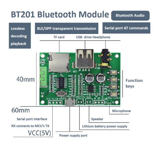
1. First, please refer to the provided BT201 test DEMO module as the standard.
2. If using the chip independently without testing the BT201 module and directly proceeding to layout, background noise is highly likely if experience is limited. Therefore, always compare with the manufacturer’s test board first.
3. The BT201 solution does not include FM functionality. Please note this. The FM circuit should be left floating without hesitation.
2.Precautions
1. Background noise or interference is common in Bluetooth audio products. Do not be careless during layout.
2. If you have not worked on audio products before, study online resources thoroughly. Assuming things casually will naturally lead to noise issues.
3. The core principle is to separate analog ground and digital ground. If unclear, consult an experienced engineer.
4. Ensure a clean power supply. Use an LDO whenever possible instead of a DC-DC converter.
5. Bluetooth operates at high-frequency RF and radiates energy, so some background noise is inevitable but can be minimized. With good design, noise is imperceptible to the human ear, though it may be measurable with instruments.
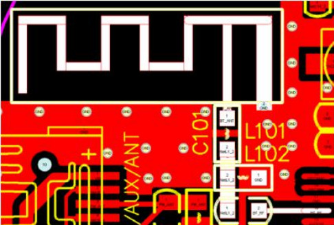
3.Antenna Description
1. For antenna and component packaging, directly refer to the PCB files of the DEMO module, available in the document library.
2. The Bluetooth antenna has no special requirements. Follow the provided package and reference instructions.
3. The Bluetooth antenna does not require impedance matching, and standard copper thickness is sufficient. Don't over complicate it—Bluetooth has a low entry barrier.
4.Power Supply Description
(1)The BT201 test board has minimal background noise, barely noticeable to the human ear.
(2)You can try powering it with a phone charger, which should not produce significant noise.
(3)Battery power is ideal as it provides pure DC and is very clean. However, consider the battery's load capacity.
(4)USB output from a desktop computer may produce significant ripple, leading to background noise. Avoid using it.
(5)If the board includes a DC-DC converter, it may cause noise. The optimal power supply is an LDO, such as a 7805.
(6)The BT201 module can drive a maximum speaker of 4 ohms, 3W with a 5V supply.
(7)When driving speakers, ensure sufficient current with a stable power supply. Insufficient current can cause speaker distortion, buzzing, etc.
(8)If possible, purchase various amplifier modules online for comparison testing. We sell Bluetooth chips, but amplifier-related noise, distortion, or other issues are extended topics that are complex and cannot be explained briefly.
5.How to check if the board has background noise?
(1)Use a clean power supply, ideally a battery, and disconnect all front-end power circuits.
(2)Connect the chip's headphone output and listen for noise. If none, check the rear-stage amplifier circuit.
(3)If USB playback has no noise but Bluetooth does, this does not necessarily indicate a problem.
(4)Use headphones to check for noise. If none, the issue lies in the amplifier section, so inspect it.
(5)If noise is present with headphones, disconnect the rear-stage amplifier and inspect the Bluetooth chip's peripheral circuits. Determine whether noise occurs during Bluetooth or MP3 playback. For Bluetooth noise, check if capacitors around the main controller are properly soldered and if they are too close to the Bluetooth module. Refer to other instructions for troubleshooting.
(6)For noise testing, avoid using a computer's USB or a charger's USB. Use a clean power supply with strong load capacity, ideally tested at 5V, not 3.7V.
6.Methods to Reduce Bluetooth Background Noise
(1)Keep the Bluetooth antenna and Bluetooth module as far as possible from analog circuits.
(2)The chip's analog ground must be connected to the power ground at the input.
(3)Check capacitors around the chip for issues such as short circuits or poor soldering.
(4)Add multiple vias to the GND of the Bluetooth section.
7.Selection and index requirements of crystal oscillators
(1)Bluetooth has high frequency offset requirements, so the crystal oscillator's quality is critical for performance. During selection, ensure consistency and stability, with a frequency deviation of ≤±10ppm and a recommended load capacitance (CL) of 12pF.
Note: Crystal-to-ground capacitors C102 = C103 = 2*CL – (4pF~6pF), where CL is the crystal's load capacitance.
(2)For designs with no size constraints, use the crystal specified in our DEMO, which is cost-effective and high-performing.
(3)For size-constrained designs, use a 24M-3225 crystal, which is slightly more expensive but performs well.
Recommendation: Use our provided crystal, which is more cost-effective and quality-assured compared to random purchases.
8.Simple PCB Layout Precautions
(1)The input voltage to LDO_IN (Pin 18 of the chip) must not exceed +5.5V.
(2)The chip must strictly separate digital GND and analog AGND (refer to the provided BT201 PCB).
(3)During PCB routing, digital GND and analog AGND must be routed separately and connected only at the battery input. If the design includes a pre-amplifier ground, connect AGND to it.
(4)All decoupling capacitors on the main controller must be placed as close as possible to the chip pins, with short ground return paths.
(5)Prioritize the placement of the Bluetooth antenna. The RF antenna must be near the board edge (or in an open area if structural constraints apply). The antenna matching circuit must be close to the RF pin, with short routing. The antenna's ground plane should follow the yellow outline in the antenna package, and the space on both sides should be as wide as possible, as shown in the diagram avove.
(6)The 24M crystal must be placed close to the chip's clock pins (BTOSCO and BTOSCI). Its routing must be shielded with a ground plane, kept away from interference sources, and not routed parallel to other data lines.
(7)Audio signal lines (DACL, DACR, AUXL, AUXR, MIC, etc.) must be routed away from digital signals (LCD/LED signals, USB, SD, etc.).
#bluetooth#audiochip#bluetoothchip#voicechip#ble#spp#electronic#coding#embeddeddevelopment#devlog#aiot
0 notes
Text
Antenna in Package AiP Market Opportunities Rising with Expansion of Millimeter Wave Technology Globally
The Antenna in Package (AiP) market is gaining significant traction as wireless communication technologies become increasingly integrated into compact, high-performance electronic devices. AiP technology incorporates antennas directly into semiconductor packages, enabling advanced radio frequency (RF) performance while saving space. This innovation is particularly relevant in 5G, millimeter-wave (mmWave), automotive radar, satellite communications, and IoT applications.

Market Drivers
One of the primary drivers of the AiP market is the global rollout of 5G technology, which operates at higher frequencies such as mmWave. These frequencies require advanced antenna solutions capable of handling high data rates and low latency. Traditional printed circuit board (PCB) antennas often fall short in terms of integration and performance. AiP offers a more efficient alternative by reducing interconnect losses and supporting beamforming technologies critical for 5G.
Another major factor is the increasing miniaturization of consumer electronics. Smartphones, wearables, and IoT devices demand compact components that deliver excellent performance. AiP technology meets this requirement by integrating the antenna and RF front-end into a single compact module, freeing up space and improving system-level efficiency.
Technological Advancements
Recent advancements in substrate materials, system-in-package (SiP) technologies, and 3D packaging are making AiP solutions more cost-effective and scalable. Low-temperature co-fired ceramic (LTCC) and organic substrates have enabled better thermal and electrical performance. Integration of multiple functions such as filters, power amplifiers, and transceivers within the package has allowed manufacturers to create multi-functional modules tailored for specific end-uses.
In addition, the evolution of advanced simulation tools and design automation has shortened development cycles and reduced costs, making AiP more accessible to a broader range of industries. These advancements have facilitated faster prototyping and more reliable testing environments.
Key Market Segments
The AiP market can be segmented based on frequency band, end-user application, and geography.
By frequency, the market includes sub-6 GHz and mmWave segments, with mmWave seeing higher growth due to its necessity in 5G and automotive radar applications.
By application, the market is divided into consumer electronics, automotive, telecommunications, aerospace and defense, and industrial IoT.
Geographically, North America and Asia-Pacific dominate the AiP landscape, thanks to the presence of major semiconductor companies and 5G infrastructure deployment.
Regional Insights
Asia-Pacific leads the AiP market due to robust electronics manufacturing ecosystems in countries like China, South Korea, Taiwan, and Japan. Government initiatives to boost 5G and smart city projects further support AiP growth in the region. North America, especially the United States, sees significant demand from telecom providers, defense contractors, and autonomous vehicle manufacturers. Europe is also emerging as a key region, driven by automotive and industrial automation applications.
Competitive Landscape
The AiP market is highly competitive, with key players including Qualcomm, ASE Group, Amkor Technology, Murata Manufacturing, TSMC, and MediaTek. These companies are investing in research and development to improve integration, reduce power consumption, and enhance RF performance. Collaborations, joint ventures, and strategic acquisitions are common strategies to gain market share and accelerate product development.
Startups and mid-sized players are also entering the space with niche AiP solutions for IoT and wearable devices, contributing to market dynamism and innovation.
Challenges and Opportunities
Despite its promise, AiP adoption faces several challenges. High design complexity, thermal management issues, and initial manufacturing costs are significant barriers. Additionally, maintaining signal integrity in densely packed modules remains a technical hurdle.
However, opportunities abound. As mmWave adoption expands and edge computing grows in importance, AiP is poised to play a pivotal role in enabling low-latency, high-speed communication across various devices and systems. The trend toward smart cities, connected vehicles, and AR/VR applications also offers long-term growth potential.
Future Outlook
The AiP market is expected to grow at a CAGR exceeding 15% over the next five years, driven by surging demand across multiple industries. Technological advancements, cost optimization, and expanding 5G infrastructure will be key enablers. As device manufacturers strive to balance performance, size, and power efficiency, AiP is likely to become a standard in RF design and packaging.
#AntennaInPackage#AiPMarket#5GTechnology#MillimeterWave#WirelessCommunication#IoTDevices#RFTechnology
0 notes
Text
Parry Technology
We specialize in delivering end-to-end embedded product solutions, guiding our customers from concept to fully manufactured products. Our expertise covers embedded system design, product engineering, and manufacturing, making us the trusted partner for Tier-1 and OEM clients seeking to reduce time-to-market while maintaining the highest standards of quality and innovation.
Engineering Services
Comprehensive Design Expertise: Delivering advanced engineering solutions across embedded systems, high-speed digital, RF, analog sensing, and power management. We support industrial, consumer, and automotive developments with high-speed & RF PCB layouts, EMI/EMC optimization, antenna matching, and application development.
Antenna Tuning
Optimized Wireless Performance: Enhancing efficiency across wireless technologies such as 4G/LTE, GNSS, BLE/Wi-Fi, and NFC. Our tuning services ensure reliable, high-performing connectivity for modern wireless devices.
Manufacturing Services
From Prototype to Production: Providing seamless manufacturing support, including prototyping, New Product Introduction (NPI), and batch production. We scale from low to high volumes, ensuring a smooth transition from design to delivery.
0 notes
Text
What Sets Apart a Great Electronics Design Engineer and a Top-Tier PCB Designer
Developing cutting-edge products requires more than just a basic understanding of electronics—it demands specialized expertise at multiple levels of the design process. While the roles of an electronics design engineer and a PCB designer often overlap, each discipline has its own set of core skills, priorities, and best practices. Understanding these differences can help companies build stronger teams and ensure both functionality and manufacturability from concept to production.
1: Foundations: Concept vs. Layout
Electronics Design Engineer
System-level thinking: Architects circuits that meet performance, power, and cost targets.
Component selection: An electronics design engineer chooses processors, sensors, power supplies, and other parts based on specifications and availability.
Simulation and validation: Uses SPICE, MATLAB, or custom scripts to verify that circuits behave as intended under various conditions.
PCB Designer
Physical realization: Translates schematic diagrams into board layouts, deciding component placement, routing, and layer stacks.
Signal integrity: Manages trace lengths, impedance control, and differential pairs to prevent timing mismatches and noise.
Thermal management: Integrates heat sinks, copper pours, and thermal vias to maintain reliable operating temperatures.

2: Technical Skills: Breadth vs. Depth
Breadth of Knowledge (Engineer)
A great electronics engineer understands analog and digital domains, power management, RF techniques, and often systems integration. Their toolkit includes:
Circuit simulation tools (e.g., Cadence, LTspice)
Firmware debugging (e.g., JTAG, SWD)
Test equipment (oscilloscopes, spectrum analyzers)
Depth of Expertise (PCB Designer)
A top-tier PCB designer goes deep into board stack-up design, advanced routing strategies, and material characteristics:
PCB CAD software mastery (e.g., Altium Designer, Mentor Xpedition)
High-speed design considerations (e.g., controlled impedance, crosstalk analysis)
3: Collaboration and Workflow
Communication Styles
Electronics engineers often work in cross-functional teams—mechanical, software, and compliance—to validate overall design requirements. Their deliverables include schematics, block diagrams, and simulation reports.
PCB designers interact heavily with manufacturing partners. They must document fabrication drawings, assembly notes, and BOM details clearly to avoid production delays.
By recognizing the strengths each role brings—and fostering close collaboration between them—teams can bring innovative, reliable products to market faster and more efficiently.
Source: https://extrondesignservice.blogspot.com/2025/05/what-sets-apart-great-electronics.html
0 notes
Text
PCB Design Driven by Precision, Practicality and Performance

At Arrival Electronics Limited, we understand that PCB design isn’t just a step in product development—it’s the foundation that supports every component, signal path, and functionality. Whether you're developing a next-generation medical device, a robust industrial control unit, or a compact consumer electronic product, our role is to ensure your ideas are backed by dependable, efficient, and expertly engineered printed circuit boards.
With decades of hands-on experience in electronics, our team has worked with companies across multiple industries, helping bring projects to life—from concept through to production.
In this article, we’ll share what makes a strong design, the practical elements that often go unnoticed, and how our services help keep your project moving forward from the drawing board to delivery.
Why PCB Design Matters
Designing the right board isn't just about connecting components—it's about ensuring the entire electrical system performs reliably, consistently, and within its intended environment. A well-thought-out layout contributes to:
Product longevity and durability
Efficient power consumption
Signal integrity and reduced noise
Thermal control and mechanical stability
Overlooking critical details during this stage can lead to performance issues, unnecessary rework, or even total product failure. We take every aspect seriously to help our clients avoid costly missteps and stay on track.
What Makes a Solid Design?
Over the years, we’ve found that strong board design depends on more than just software skills or technical knowledge. It’s about having the awareness to balance practical considerations with real-world requirements. Here’s what we focus on in every project:
1. Clear Design Objectives
Before a single trace is laid out, we work closely with you to understand the end-use of the product. Is it intended for a high-vibration environment? Will it operate at high frequency? These questions shape everything from component selection to board layout.
2. Efficient Layout and Routing
We pay close attention to the physical layout, making sure component placement allows for clean, short signal paths and minimal electromagnetic interference. Where needed, we apply differential pair routing, impedance control, and strategic layer stacking.
3. Manufacturability
A design that’s difficult to produce can quickly eat into budgets and timelines. We align our designs with your manufacturing capabilities—choosing standard sizes, spacing, and materials that avoid bottlenecks in production.
4. Thermal Management
Heat can quietly cause long-term damage. We integrate copper pours, thermal vias, and heat sinks when necessary, ensuring temperature-sensitive components stay within safe operating ranges.
5. Design for Testability
We keep diagnostics in mind from the outset. Well-placed test points and clearly labelled nets allow engineers to easily validate performance and troubleshoot issues during development.
Our Approach
What sets us apart is the level of care and accountability we bring to each project. We don’t treat board design as a one-size-fits-all task. Instead, we tailor our process to match your product’s specific technical and commercial requirements.
Collaborative from the Start
We believe good design starts with good communication. Our team begins by understanding your specifications, timelines, and constraints. If needed, we assist with component selection and design reviews, helping guide decisions that support project success long-term.
In-House Expertise
Our engineers bring decades of collective experience across RF design, digital and analogue electronics, signal integrity, and power distribution. This depth of expertise means we’re equipped to handle both complex multilayer PCBs and simpler single-sided designs with the same level of detail and reliability.
Detailed Documentation
We provide comprehensive documentation for every design, including Gerber files, BOMs, assembly drawings, and test documentation. Everything is clearly structured, so your production team or manufacturer has what they need to get started without delay.
Supporting Every Stage of Development
We understand how interconnected the design process is with the rest of the product lifecycle. That’s why our support doesn’t end once the board layout is finished.
Prototyping
We help bridge the gap between design and validation by assisting with prototype builds. If changes are needed, we provide quick iterations without compromising design integrity.
Compliance
Many products need to meet specific regulatory standards. Our knowledge of EMC, safety, and industry certifications helps keep your project aligned with compliance from the ground up.
Component Availability
Supply chain challenges can affect even the most carefully engineered layouts. We actively review component availability early in the process and suggest practical alternatives when necessary. This helps keep your project on schedule and reduces the risk of unexpected delays.
A Closer Look at Our Capabilities
Here’s a snapshot of the types of board layout work we handle:
Single-sided and double-sided configurations
Multilayer builds (up to 24 layers)
High-speed digital and analog signal routing
RF and microwave applications
Flexible and rigid-flex formats
Power distribution and regulation paths
Projects with tight impedance and signal integrity demands
All layouts are created using industry-standard tools, including Altium Designer and Cadence Allegro, ensuring smooth integration with your existing workflows.
Industries We Serve
One of the strengths of our team is our versatility. We’ve worked with clients across sectors including:
Medical Technology: Supporting devices that require extreme reliability and precise electrical behavior.
Industrial Automation: Creating robust PCBs for use in high-temperature, high-vibration environments.
Consumer Electronics: Helping bring compact and functional designs to market faster.
Automotive: Designing for safety, efficiency, and long-term performance in vehicle systems.
Telecommunications: Handling high-frequency signal requirements and tight timing constraints.
No matter the application, we bring the same level of care and engineering discipline to every project.
Focused on Accuracy
Every layout we deliver goes through rigorous design rule checks (DRC), electrical rule checks (ERC), and internal peer reviews. We follow industry best practices and adapt our quality assurance process to meet the specific standards of your sector.
We’ve earned the trust of clients across the UK by consistently delivering high-quality work with a personal touch. Our focus is on making your project a success—not just through technical execution, but through reliability, responsiveness, and genuine collaboration.
Common Challenges We Help Solve
If you’ve experienced any of the following issues, we’re here to help:
Designs that aren’t manufacturable without rework
Unstable prototypes or unexpected signal behaviour
Thermal problems during test or usage
Poor EMI performance or compliance failures
Designs delayed by long lead-time components
The Edge of Partnering With Us
There are many design services out there. What makes us different is the way we treat our clients and the projects they entrust to us. When you work with us, you get more than a technical service—you gain a partner who’s committed to your success.
We listen. Your needs guide every design decision we make.
We respond quickly. Tight timelines don’t faze us—we’re used to working in dynamic environments.
We follow through. From first sketch to final sign-off, we’re with you every step of the way.
Whether you’re a start-up developing your first prototype or an established manufacturer needing dependable support for your next product line, we bring the right mix of experience, care, and clarity to help you move forward.
Let’s Begin Your Project
IIf you're looking for dependable design services with a team that understands the real-world pressures of product development, we’re here for you at Arrival Electronics Limited. Our process is built around clear communication, careful planning, and engineering you can trust, including expert PCBA services to ensure every component is perfectly integrated.
We’re more than just a distributor—we’re your engineering partner. From bespoke solutions to component sourcing and full system support, we’re here to help turn your vision into reality.
For more about our services or to start a conversation, visit arrivalelectronics.co.uk.
0 notes
Text
Choosing the Right PCB Material: A Comprehensive Guide | PCB Power

Choosing the Right Printed Circuit Board Material: A Comprehensive Guide
The choice of materials commonly used for the fabrication of the PCB is extremely important in determining the quality of it. The selection of PCB base material can impact electrical properties, thermal and mechanical behaviour, and reliability of the final product. In this blog, we will learn about the printed circuit board materials which are available to the buyers and their characteristics.
Common Types of PCB Materials
A list of the most common printed circuit board material is given below:
1. FR-4
FR-4 is the most common substrate material for making multi-layer printed circuit boards. It is a fibreglass-epoxy composite, with high dielectric strength. The material FR-4 can retain its stability up to the temperature of 130°C (266°F). It is used in consumer electronics, industrial control, telecommunications and other general application gadgets.
2. Polyimide
Polyimide is famous for its heat resistance and flexibility characteristics. It is commonly applied to flexible PCBs, where the board can be bent or folded. For example, in the case of a smartphone design. Polyimide can work up to a temperature of 260°C (500 °F). It is appropriate for aerospace, automobile, and medical devices where high performance is required.
3. Metal Core PCBs
Metal core PCBs are designed with a metal base material, often aluminum or copper. It offers five times better heat dissipation than FR-4 boards. These boards are popular in areas of heat dissipation which may include LED lighting and power electronics. Metal core PCBs have better thermal management under thermal loads.
4. Rogers Materials
Rogers Corporation produces a range of high-frequency materials that are suitable for advanced applications requiring precise electrical performance. Rogers materials provide low-loss characteristics and stable dielectric constants across varying frequencies.
They are used in telecommunications, aerospace, and military applications.
5. Taconic TSM-DS TLY-5 & DS3
Taconic TSM-DS TLY-5 and DS3 are specialized PCB materials intended for high-frequency applications. They are characterized by low dielectric constants and loss tangents, which keep the signal integrity at RF and microwave frequencies. Taconic materials are used in telecommunications and automotive radar.
Factors to Consider While Choosing PCB Materials
These are some factors one must consider before selecting the material for a printed circuit board:
1. Material Type and Properties
The choice of PCB material significantly impacts its functionality and reliability. Understanding the properties of the materials, such as dielectric constant (Dk), loss tangent (Df), and thermal expansion coefficient (CTE), is important.
2. Thermal Management
If there is heat involved, then thermal performance is very important, especially for high-power applications. The main thermal properties to study are as follows.
Glass Transition Temperature (Tg): At this temperature, the material would go from being a rigid state to more flexible. Thus, higher Tg materials are better to be used at high temperatures.
Decomposition Temperature (Td): It is the temperature at which the material will begin decomposing. Better indications under very difficult conditions are seen in higher Td.
3. Manufacturing Process Compatibility
The chosen material should also correspond to the manufacturing method employed, i.e., through-hole or surface mount technology (SMT). For example, SMT relies on FR-4 for favourable drillability, while flexible PCBs need materials such as polyimide, which don't crack during bending.
4. Environmental Considerations
Always evaluate the PCB's operational condition since humidity, temperature rise and fall, and exposure to chemicals influence the selection process of materials. Ensure the selected materials can withstand these conditions without degrading.
5. Frequency Range
In an instance where high-frequency signals are involved, it is critical to select materials that have low dielectric loss. High-speed PCBs may require special material under this.
Conclusion
Choose the right printed circuit board material to get the best result in the electronic designs. Designers must know about the properties of various materials such as FR-4, polyimide, PTFE, metal core, and Rogers to satisfy the needs of the projects. Electrical behavior, thermal properties, mechanical strength, cost ,and feasibility of PCB fabrication during manufacturing will help you decide which material is most suitable for your particular project.
At PCB Power, we manufacture high-quality printed circuit boards crafted from a variety of materials, including FR-4, polyimide, and metal core. Whether you are looking for prototype circuit boards or need them in volume, PCB Power can be your trusted partner
Contact our team of experts to discuss your requirements.
Know More: https://www.pcbpower.us/blog/choosing-right-pcb-material-guide
0 notes