#Two layer pcb stencil
Explore tagged Tumblr posts
Visit Tumblr Blog
Explore Tumblr blogs with no restrictions, modern design and the best experience.
Last Seen Tumblr Blogs


Fun Fact
Tumblr posted its first advertisements in May 2012 and subsequently earned $13M in revenue.
Text
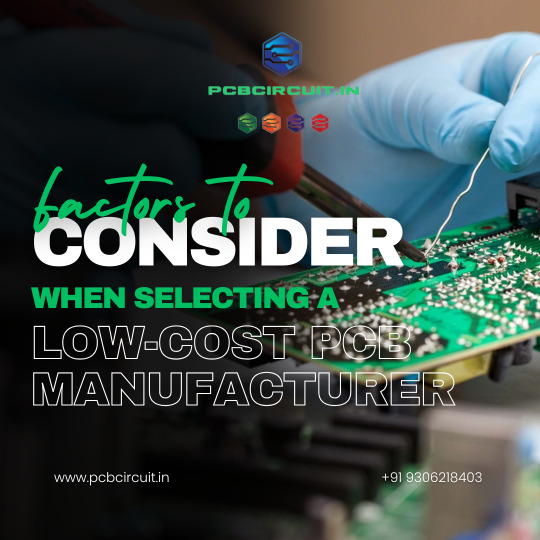
Factors to Consider When Selecting A Low-Cost PCB Manufacturer
Choosing the right low-cost PCB manufacturer can be challenging, especially with many available options. To help you make an informed decision, we've outlined five key factors to consider when selecting a low-cost PCB manufacturer.
#custom pcb manufacturing#pcb fabrication#pcb manufacturer in india#prototype pcb manufacturing#pcb manufacturer#two layer pcb stencil#pcbcircuit#best pcb stencil maker in hyderabad#pcb manufacturer in delhi#pcb manufacturer in maharashtra
0 notes
Text
Benefits of Multi-Color PCBs in Circuit Design
Multi-color printed circuit boards (PCBs) are transforming the landscape of electronic design by blending functionality with aesthetics. One of the primary benefits of multi-color PCBs is that different colors can indicate specific circuit functions or components, helping engineers and technicians quickly identify issues during manufacturing and testing. , the use of multi-color PCBs can improve thermal management and signal integrity

#PCB manufacturer#PCB fabrication In india#custom PCB manufacturing in india#prototype PCB manufacturing#low-cost PCB manufacturer#high-quality PCB manufacturing#quick turn PCB fabrication#flex PCB manufacturer#multilayer PCB manufacturer#Best pcb manufacturer#Top 10 pcb manufacturer#Pcb manufacturer near me#Pcb manufacturer in Maharashtra#Pcb manufacturer in haryana#Pcb manufacturer in delhi#Pcb manufacturer in india#Pcb manufacturer in Bombay#Pcb manufacturer in jaipur#Best pcb assemble in hyderabad#Low cost pcb assembled in hyderabad#Good pcb assemble in hyderabad#Free sample pcb assemble in India#pcb stencils#Two layer pcb stencil
0 notes
Text
SMD PCB Board Assembly in Hyderabad - Pcbcircuit
SMD is also known as Surface Mount Device. It is an electronic device. SMT (Surface Mount Technology) is the technique that is necessary for the production of SMDs on a large scale. Being a well-established organization, we are offering SMD PCB Board Assembly in Hyderabad . We have team of experts for procurement of high-quality low-cost electronic components while rendering this PCB manufacturing service.

#Pcbcircuit#PCB Manufacture#low-cost PCB manufacturer#PCB fabrication#custom PCB manufacturing#Pcb manufacturer in india#Pcb stencil#Two layer pcb stencil
0 notes
Text
Best Two-layer PCB Stencil For Solder Paste
Our high-quality two-layer PCB stencil is designed for precise solder paste application, ensuring accurate and clean surface-mount component placement. It features fine apertures for perfect paste deposition, enhancing soldering reliability and reducing defects. Ideal for small to medium production runs, it guarantees efficient assembly with consistent performance.

#custom pcb manufacturing#pcb manufacturer#prototype pcb manufacturing#high-quality pcb manufacturing#flex pcb manufacturer#multilayer pcb manufacturer#quick turn pcb fabrication#low-cost pcb manufacturer#pcb fabrication
0 notes
Text
Printed Circuit Board Assembly (PCB Board Assembly): The Heart of Modern Electronics
Printed Circuit Board Assembly (PCBA) is a significant cycle in the assembling of electronic gadgets, where electronic parts are mounted and associated with a printed circuit board (PCB). The majority of electronic devices are built on PCBs, which provide the mechanical support and electrical connections necessary for the device to function. The gathering system changes an uncovered PCB into a completely utilitarian board that can be utilized in many applications, from buyer gadgets to modern hardware.
The PCB Assembly Process There are several steps in the PCB Assembly process, all of which are necessary to guarantee the quality and functionality of the final product:

1. Solder Paste Application: The most important phase in PCB gathering is applying bind glue to the region of the PCB where parts will be put. A stencil is utilized to apply the patch glue precisely to the PCB cushions, which are regions where the part leads will interface.
2. Part Situation: After the bind glue is applied, the electronic parts are put on the PCB. Pick-and-place machines, which are automated machines that can quickly and precisely position thousands of components onto a PCB, are typically used for this. Parts utilized in PCBs incorporate resistors, capacitors, coordinated circuits, and connectors.
3. Soldering: To ensure a strong electrical connection, the components must be soldered after being placed on the PCB. There are two chief restricting techniques used in PCB gathering: reflow restricting and wave welding. Wave soldering is used for through-hole components, whereas reflow soldering is commonly used for SMT components.
4. Inspection and Testing: The assembled PCB is examined for flaws such as solder bridges, misaligned components, and incomplete solder joints following soldering. Robotized Optical Review (AOI) and X-ray assessment are usually utilized for this reason. Additionally, functional testing is carried out to guarantee that the PCB will perform as intended in the final application.
5. Final Assembly and Packaging: The last move toward the PCB gathering process is the last get together and bundling. This might include adding heat sinks, fenced in areas, or connectors, and setting up the board for transportation.
Significance of PCB Assembly
PCBA is basic since it straightforwardly influences the exhibition, dependability, and life span of electronic gadgets. A very much gathered PCB guarantees that the gadget works accurately and can endure the afflictions of its expected use. Failures caused by poor assembly can be costly in terms of customer satisfaction, replacement costs, and repairs.
PCB Board Assembly is made even more difficult by the complexity of contemporary electronics, which are becoming smaller and more functional. To meet the increasing demands for improved performance and miniaturization, cutting-edge assembly methods like multi-layer boards and high-density interconnects (HDI) are now commonly used.
In conclusion, the production of electronic devices relies heavily on the Printed Circuit Board Assembly procedure. PCBs are the foundation of all modern electronics, from smartphones to industrial controllers. Understanding the PCB get together cycle is essential for anybody engaged with gadgets plan and assembling, as it assumes a significant part in guaranteeing the usefulness and dependability of the eventual outcome.
1 note
·
View note
Text
ASRock X670E Steel Legend Wi-Fi Update

Well-connected ASRock X670E Steel Legend Wi-Fi update
ASRock’s X670E Steel Legend Wi-Fi is our next (and maybe last) AMD X670 evaluation on our current platform. We tested all Intel and AMD Steel Legend boards, ending with the X670E. The black, silver, and grey design has four M.2 sockets, four SATA ports, PCIe 5.0 (slot and socket), two NICs, and integrated Wi-Fi 6E. Finally, high-quality audio is provided.
As this platform progressed, ASRock offered five X670 SKUs. The top-of-the-line Taichi and Taichi Carrara, the mid-range Steel Legend, and the economical PG Lighting and Pro from X670 are available. For a smaller MicroATX or MiniITX form factor, use the B650 chipset or A620 boards. ASRock AM5-based motherboards include several features.
Most tests showed the X670E Steel Legend was average to above average. We saw its fastest performance in Procyon Office and gaming testing. Long-running multi-threaded functions are no problem for VRMs. Performance is fine out of the box.
Below, we’ll examine the board’s features to determine its place on our Best Motherboards list. Before we discuss testing and boards, we’ll list ASRock’s website specs.
Specifications: ASRock X670E Steel Legend Wi-Fi
Inside the ASRock X670E Steel Legend Wi-Fi Box
Inside the package, on a cardboard barrier on top of the motherboard, are some accessories to get you started without shopping. The user manual, two SATA cables, four M.2 screws/standoffs, and Wi-Fi antenna are included. For heavier video cards, ASRock supplies a motherboard graphics card holder.
Design of the ASRock X670E Steel Legend Wi-Fi
ASRock calls the Steel Legend a “philosophical state of rock-solid durability and irresistible aesthetics.” Black 8-layer PCBs with huge silver heatsinks and stencilled black-and-gray (nearly camouflage) design components target mainstream enthusiasts. The chipset and left VRM bank have Steel Legend branding, but it doesn’t light up like other SKUs.
Two RGB LED strips are on the X670E Steel Legend. One illuminates the Steel Legend branding on the chipset heatsink on the bottom of the board, while the other dwells under the SATA ports on the right edge. Bright LEDs and vivid colours create a light display inside your chassis. We appreciate the neutral aesthetic, which matches most build themes, but the board won’t win any awards.
Top half: The left VRM heatsink has a lot of mass and surface area to keep MOSFETs underneath running within spec. ASRock and Steel Legend branding and chipset mention are on top. Processor power comes from two 8-pin EPS connectors above the heatsinks (one required).
We encounter the first of six four-pin fan headers underneath the left VRM heatsink before moving right. The placement may seem odd, but it’s ideal for chassis rear fans. PWM and DC are supported by all fans. The CPU FAN1 can output 1A/12W, while the rest can handle 2A/24W. There’s enough power for fans or a custom water loop with fans and a pump.
After the socket, we find four reinforced DRAM slots with a top lock. Up to 192 GB of DDR5–7600 memory is supported. Our DDR5–5600 and DDR5–6000 kits worked OK, however our Temagroup DDR5–7200 kit didn’t, even though a faster (7600) kit with more capacity is mentioned. You’ll be fine with memory QVL kits.
Two more 4-pin fan headers are above the memory slots. Next, we see the first two 3-pin ARGB headers (the other and one RGB header are along). ASRock Polychrome Sync controls these devices.
The 4-LED Post Status Checker appears as we go down the right edge. The POST procedure illuminates the CPU, DRAM, VGA, and Boot LEDs. The LED stays lit if there’s a problem in one of those regions, giving people a basic sense. We then encounter the board’s 24-pin ATX connector, a 19-pin front panel USB 3.2 Gen 1 (5 Gbps) connection, and a Type-C connector.
X670E Steel Legend VRMs have 19 phases, 16 of which are Vcore. From the 8-pin EPS connectors, power goes to the Renesas RAA229628 20-phase PWM controller and the 16x 60A Intersil ISL99360 SPS MOSFETs. As with other boards with the similar setup, the 960A wasn’t the most powerful, but it handled our flagship Ryzen 9 7950X chip without issue.
On the lower left, the audio component shines. Three yellow audio capacitors and the Realtek ALC1220 codec are visible. No Faraday cages or sophisticated DACs/Amps, but the audio solution is fine for most people.
Midboard has three PCIe slots (two full-length and one x1) and four M.2 connectors. Top PCIe slots connect through the CPU to PCIe 5.0 x16. Through the chipset, the bottom full-length socket supports PCIe 3.0 x4. If you like multi-GPU systems, these two slots support AMD Crossfire. The tiny open-ended x1 slot uses chipset lanes and supports PCIe 3.0 x1. Understand your hardware needs and if PCIe 3.0 speeds limit them with these slots.
Four M.2 sockets surround the PCIe slots. Top socket M2_1 is your processor-connected PCIe 5.0 x4 (128 Gbps) socket. The rest connect through the chipset and run at PCIe 4.0 x4 (64 Gbps) with 80mm module support per socket. The right edge has four SATA ports. All SATA and M.2 ports support RAID0/1/10. Storage is abundant, especially M.2.
Many headers are revealed on the board’s bottom. Additional USB connections, RGB headers, and power/reset buttons are standard. A complete left-to-right list follows.
Audio front panel
RGB 4-pin header
3-pin ARGB header
5-pin Thunderbolt AIC connector
(2) System fan headers
Clear CMOS jumper
(2) 2.0 USB headers
Fan system header
Talker heading
Panel header
Like most high-end models, the X670 Steel Legend’s motherboard has a back IO plate. It has the same black, white, and grey background and black labels as similar boards. However, the back IO has 12 USB slots. Plenty of ports include a USB 3.2 Gen 2×2 (20 Gbps) Type-C port, a Type-A port, six Gen 1 (5 Gbps) connections, and four USB 2.0 (480 Mbps) ports. HDMI and DisplayPort ports are for video, whereas 2.5 GbE and 1 GbE are for networking. Also present are Wi-Fi 6E antenna connectors. Last, the audio stack has two analogue and SPDIF ports.
0 notes
Text
PCB assembly for dummies: A step by step guide to getting PCB assembly right
Before many years, food, shelter & water were the essential part for an individual in their day to day lives, but now one major factor is added that is electronics. Our day starts with electronic components and ends with the same, from our phones to our cars to our home appliances. And the most essential part of these electronics is the printed circuit board (PCB).
What is PCB?
So you may have come across the small green chips may be in your phone, or say TV remote covered with copper parts and lines, these tiny green coloured chips are PCB, & they form the heart of that particular electronic device.
The output of the green colour:
The PCB comprises of copper lines, fiberglass, and other metal parts, and these boards are joined together with epoxy and insulated with a solder mask. And from this solder mask, the green colour comes from.
You may have also observed these boards with components firmly stuck on it and for an advanced PCB to work efficiently, the components should be perfectly mounted on it. And a PCB with organised components on it is called an assembled PCB. And the process of manufacturing is called PCB assembly or PCBA.
Do you have any idea about how these devices are made? The process of PCB assembly is an easy one but has many manual and automated steps. Every step, the manufacturer has an option to select from an automated and manual process. Yeah, this is quite confusing, to let’s make this easier and have a look at the below steps from the initial stage to the end with a brief explanation.
The PCBA Process steps:
1. Solder Paste Stencilling
So the processing of the PCB assembly starts with applying a solder paste to the board. It’s similar to the process of screen printing, wherein a thin stainless steel layer of the stencil is placed over the PCB. The assemblers apply the solder paste only to fixed parts of the future PCB, &only the components will be placed when the PCB is completed.
Image Source: https://www.pcbcart.com
So the solder paste is to be applied evenly on the circuit board, and also in the intended locations where it should be needed.
2. Pick and Place
Once you have applied the solder paste to the PCB board, the process of PCBA is taken to a further step and that is the pick and place one. The PCB board is picked with a vacuum grip and placed on a machine and a surface mount components or SMDs are applied on the prepared PCB with the help of a robotic device. And in the later stage, these SMDs are soldered on the surface board.
Before the invention of machines, this step was manually done with the help of tweezers, & here the assemblers had to pick and place all the components with hands. But thanks to the machines, to make them work for the humans quite simpler and easy.
3. Reflow Soldering
Now when the solder paste and SMD have been placed, they also have to be solidified, to keep the paste and components to remain in their place. And the PCB assembly is skilled through a process called “reflow”.
After the completion of the Pick & Place process, the PCB board is shifted to a conveyor belt. The belt takes the PCB board to a large reflow oven, the oven has many inbuilt heaters & these heaters in turn heats the board to the temperature to around 250 degrees Celsius. The solder is melted into the solder paste with the immense heat in the oven.
As the solder starts to melt, the PCB moves through the oven and is passed through coolers, and this cools the melted solder and solidifies in a controlled manner. And in the end the SMDs are connected to the PCB with the creation of a permanent solder joint.
4. Inspection and Quality Control
Once the reflow process is done, we need to check the quality and conduct an inspection, and at this time the mount components are already soldered into a place. This assembled board is inspected for knowing the functionality.
Manual checks: This is done by an assigned designer, who visually ensures the quality and functionality of a PCB.
Though you come across any mistake or not, you need to carry on the next step that is to check the part and ensure the working of the same as required it to be. This means you have to check the PCB connections for quality purposes. You can carry out these inspections on regular basis to have an error-free working of the board.
5. Through-Hole Component Insertion
Once we pass the inspection stage, the board may add on more components apart from the SMDs, and this includes the plated through-hole components or can be said PTH components.
To explain PTH, it can be said that it is simply a hole in the PCB which is fully plated through the board. Now through these holes, PCB components pass the signal from one side to the other side of the board. And the soldering paste will be not the preferred one, in this case, instead, we need a step higher soldering method for the PTHs. There are mainly two main soldering methods:
Manual Soldering: This is completely manual, through-hole insertion
Wave Soldering: This can be said to be the machinery form of soldering, but with a little different process. Here the PTH component is put in place and the board on the other conveyor belt. The waves of the molten solder are washed from the downwards side of the board at a stroke, and this process is undertaken with the help of the oven specially meant for this process.
6. Final Inspection and Functional Test
The last step is the final inspection which tests the PCB regarding its functioning. This is known as the “functional test”. How the PCB is operated in normal situation is tested here by putting the PCB going through many paces. Simulated signals & power pass through the PCB during the test and the electrical characteristics of the PCB are tested.
If any problem faced in the current or signal output, voltage, or any unacceptable fluctuation occurs, then the PCB fails the test. This failed PCB can be later recycled or whatever are the company laws.
But testing is one of the step not to be missed in the PCB assembly process,as the pros and cons is decided in this stage only.
So widely choose your PCBA manufacturer like Jayshree Instruments that delivers the best services and assuring PCB assembly process meets the high quality standards and work.
2 notes
·
View notes
Text
The best SMT machine manufacturers for all your needs
Surface Mount Technology (SMT) is quickly taking over through-hole printing procedures in the design and manufacturing processes of PCB boards. It has largely to do with the increased control over when size, weight, and automation since SMT can create PCBs a lot more effectively without losing any dependability or quality. This innovation has gained popularity with the creation of PCBs for gadgets that were not recently considered reasonable or conceivable.
SMT utilizes surface mount gadgets (SMDs) to supplant the parts used in TH PCB development. Essentially all gear that is created today involves surface mount technology for its many benefits during PCB production. Increasingly more PCB gadgets are accessible as SMDs or bundles, which makes the reception of SMT incredibly pragmatic and practical. SMT board development makes a more proficient, automated PCB development process for large-scale manufacturing.
The most noteworthy advantages of SMT manufacturing incorporate increased automation of procedures, greater adaptability in building PCBs, further enhanced quality and execution, decreased manual intercession for part arrangement, complete elimination of drill hole activities, more hi-tech, lighter sheets, simplicity of assembly, utilizing the two sides of the board without the limitations that exist in the through-hole design, capacity to coincide with through-opening parts, even on a similar board.
SMT Manufacturing processes are on the rise
SMT manufacturing also provides expanded utility with more SMD parts in a similar space, or a similar number of parts in a lot more compressed space. Manufacturing for the most part comprises a few exceptionally mechanized processes for SMT manufacturing, including essential advances. The board material contains patches without openings and weld glue is applied with a screen-printing-like interaction.
The position is controlled through an exact stencil layout for the particular PCB being manufactured to guarantee the material is just applied where required. SMT machines purchased by leading SMT machine manufacturers then position the ideal SMDs and different parts on the sheets exactly. They are placed into the machines on reels or tapes. Sheets then proceed to patch activities which heat the pads to where the applied weld glue melts and bonds the parts to the board.
In circumstances where the two sides of the printed circuit board are being used for parts, the processes are redone for the other side. Any sensitive parts integrated on the PCB might be introduced after the mechanized patching, either physically or through processes that wouldn't harm the part. Sheets are then "washed" to eliminate abundance transition or patch buildups that could make shorting of parts due to their incredibly close placement.
SMT can fit your requirements in the best way
When the items are done, cleaned, and dried, they are prepared for definite investigation. Investigations search for missing parts, arrangement issues, or patching issues that could create likely issues. There is hardware accessible to automate these assessments. Assessed sheets then continue to any necessary testing of circuits and usefulness. SMT is an adaptable and strong gathering process that has permitted manufacturers to create current gadgets with the best technology.
In SMT, every one of the various parts required for the present gadgets is appended to the outer layer of the printed circuit board. SMT can be exceptionally computerized, it is undoubtedly the best fit for clients needing circuit sheets in high volume, but at the same time, it's profoundly adaptable. If you want circuit sheets collected to meet extraordinary prerequisites, SMT might be the most ideal decision.
Find the right SMT machinery for your needs at Southern Machinery (SMTHELP)
Southern Machinery (SMTHELP) is a longstanding SMT machine manufacturer and PCB assembly line supplier that has provided products that have proven to be useful for clients in the scope of ventures. We have spent significant time in manufacturing and have broad involvement in creating equipment for a great many applications. With a wide scope of gear and expert staff, we can help with item prototyping and testing, and contract assembling and that's just the beginning.
Surface mount boards are additionally quicker and simpler to gather and more budget-friendly than sheets developed with through-hole innovation. Through-hole PCB gathering is a more established innovation that includes joining prompts openings penetrated the circuit board. This cycle makes truly strong items, as these bondings are very durable. It tends to be more costly than SMT, however, and the density is higher. Our team can assist you with figuring out which equipment best accommodates your case.
0 notes
Text
Why choose PCBA for custom PCB assembly in 2022
PCB Terminology: Definitions You Can Use There’s a lot more to PCB design terminology than PCB vs. PCBA. Here’s key PCB terminology to become familiar with:
Double-sided PCB: also known as a two-layer PCB, a double-sided PCB features components for connectivity on both sides.
Flexible PCB: a flexible printed circuit board is designed to move and bend to accommodate the design of the device. Flexible PCBs provide OEMs with more compact, lightweight and customizable solutions to suit their needs.
FPGA: a field-programmable gate array (FPGA) is an integrated circuit that can be programmed to execute one or more operations.
FR4: low-cost printed circuit board material commonly used for the substrate layer. FR4 is made from fiberglass cloth that has been embedded in epoxy resin. The term FR4 is a type of substrate, and also the rating used grade epoxy laminate sheets.
Gerber File: computer-aided manufacturing (CAM) file used to provide an industry standard for communicating board specifications with multiple manufacturers.
Light engine: similar to a PCBA, a light engine is a small board that contains a combination of LED modules and an LED driver.
Multi-layer PCB: a board that features more than two conductive metal layers. Multi-layer PCBs enable a range of interconnections ideal for many applications and industries.
Pad: the connection point for the electronic component terminal in the PCB. Components are soldered to the pad.
Rigid PCB: the opposite of a flexible PCB, a rigid circuit board made of a solid substrate material such as metal or FR4 that can not bend. Depending on the design of the device, rigid PCBs can be the most cost-effective solution for mass production.
Single-sided PCB: a simple board with electronic connections on one side.
SMT Pick and Place Machine: High-speed, automated equipment used to place surface-mount technology (SMT) devices onto a printed circuit board. These machines are highly precise and efficient, helping reduce the costs of PCB production.
Solder Paste Printing: using a printer and a stencil, solder paste is applied to a PCB and baked in an oven to seal the bond.
Substrate: the material used to create the foundation of the PCB. This base material is usually made of fiberglass, but can also be comprised of epoxy, metal, ceramic or other materials. The material selection of the substrate is dictated by the primary function and design of the PCB and its components.
Stencils: used to aid the application of solder paste to surface mount (SMT) component pads during the printed circuit board assembly (PCBA).
Wave Solder Machine: wave soldering is a bulk soldering process used in the manufacture of printed circuit boards. The wave solder machines move each board into a pan where a wave of melted solder covers it, bonding all the components of the board together.
https://www.kingfordpcb.com/technology-blog/why-choose-pcba-for-custom-pcb-assembly-in-2022/
0 notes
Text
How To Solve Missing Paste Printing and Less Tin in SMT Assembly?
Causes of SMT Assembly missing paste printing and less tin

1. The principle of solder paste printing
The solder paste is squeezed into the stencil through a scraper so that the solder paste contacts and adheres to the PCB surface. Then the solder paste that adheres to the PCB surface during demolding overcomes the resistance of the stencil wall and is transferred to the PCB surface.
2. Observe, think & compare
A>Although part of the substrate around the pad is covered by the stencil opening during printing, the solder paste at the bottom of the stencil opening is still difficult to contact the PCB pad and the surrounding substrate. As a result, it is not enough to overcome the hole wall during demolding. Resistance (Eg. Only a small amount of solder paste on the pad)?
B>There is a 35 um deep annular pit between the pad and the solder mask. Does the solder paste with the stencil opening on the pit not touch the bottom of the pit?
C>Why are other pads connected to the circuit not easy to miss?
3. Bare copper plate printing verification
The solder paste of 5 different brands of 4# powder can be stably tinned (laser + electro-polished stencil ) on a circular hole with a thickness of 0.1 and an opening diameter of 0.28.

Solutions of SMT Assembly missing paste printing and less tin
1. Find all the pads that are not connected to the outer circuit, change the size of these pads from the original circle with a diameter of 0.27 to a circle with a diameter of 0.31; Also, reduce the area of the deep pit around the pad, and make the original opening area on the deep pit become on the copper foil of the pad, so that the gap between the opening area on the deep pit and the bottom of the stencil is reduced. After the small batch verification is OK, the original stencil is used for mass production, and the soldering of the soldering pads that are difficult to solder is good (the area of the soldering pad is increased, and no poor soldering is found in the batch verification);
2. Reduce the PCB solder mask thickness and the influence of the higher height solder mask layer on the circuit near the pad. Generally, it is recommended that the PCB solder mask thickness should be less than 25um.
3. The new PH stencil is used to eliminate printing gaps to the maximum extent. PH stencil is introduced.

Grande’s SMT Assembly Advantages
1. Strength Guarantee
▪ SMT factory: With imported SMT machines and multiple optical inspection equipment, which is able to produce 4 million points per day. Each process is equipped with QC personnel who will keep an eye on product quality.
▪ DIP production line: Two wave soldering machines and more than 10 employees who have worked for over three years. That’ s to say, these workers are highly skilled and can weld various SMT & DIP components.
2. Quality Assurance With High Cost Performance
▪ High-end equipment can paste precision special-shaped parts, BGA, QFN, 0201 package. It can also be soldered prototype pcba via SMT machine and placing bulk materials by hand.
▪ Both samples, small and large batches can be produced. And there is no SMT Machine starting cost.
3. Rich Electronic Products SMT Soldering Experience With Stable Delivery
▪ Accumulated services to thousands of electronics companies, involving SMT soldering services for various types of automotive equipment and industrial control motherboards. Furthermore, PCBA products are often exported to Europe and the United States, and the quality is able to be affirmed by new and regular customers.
4. Strong Maintenance Ability & Reliable After-Sales Service
▪ The maintenance engineers have sophisticated experience so that those defective boards caused by all kinds of smt soldering can be repaired. Meanwhile, ensuring the connectivity rate of each circuit board also make sense.
▪Order problems feedback will get response, solution and solved as soon as possible.
http://www.58pcba.com/index.php?id=1117
#smt assembly#pcba manufacturing#EMS Company#printed circuit board assembly#electronics manufacturing services
0 notes
Text
India's Trusted PCB Stencil Suppliers for Electronics Manufacturing
Explore precision and reliability with India’s trusted PCB stencil suppliers. Our stencils ensure accurate solder paste application, enhancing the efficiency and quality of your electronics manufacturing. Designed for various PCB types, we provide solutions tailored to your needs. Partner with us for exceptional stencils that deliver flawless results every time.

#custom pcb manufacturing#pcb fabrication#pcb manufacturer in india#prototype pcb manufacturing#pcb manufacturer#two layer pcb stencil#pcbcircuit#best pcb stencil maker in hyderabad#pcb manufacturer in delhi#pcb manufacturer in maharashtra
0 notes
Text
Level Up Your PCB Assembly With Next Gen Two Layer Stencils
Precision is everything in today’s fast-paced electronics world. Two-layer PCB stencils offer high accuracy and consistent solder paste application, ensuring top-notch performance for your designs!

#top 10 pcb manufacturer#pcb fabrication#quick turn pcb fabrication#pcb stencil#low-cost pcb manufacturer#pcbcircuit#flex pcb manufacturer
0 notes
Text
Top PCB Design with Two-Layer Stencils
Precision and efficiency in your PCB design with an advanced two-layer PCB stencil with pcbcircuit. These stencils ensure accurate component placement and soldering, leading to higher-quality boards and reduced manufacturing errors. Ideal for complex circuits, they streamline your production process, saving time and enhancing overall performance.

#custom pcb manufacturing#pcb manufacturer#prototype pcb manufacturing#flex pcb manufacturer#low-cost pcb manufacturer#high-quality pcb manufacturing#pcb fabrication#multilayer pcb manufacturer#quick turn pcb fabrication
0 notes
Text
Detailed guided on PCB Panel utilization
The PCB Panel benefit
A composite of printed circuit boards, i.e. Printed circuit boards that are not isolated are firmly fixed and the assembly of the printed circuit board also belongs to it, is generally taken as a printed circuit board benefit. The beauty of the layout designs must be the design of the printed circuit board use, in order to be able to use the printed circuit boards at optimal costs and stocks and configurations. The influence of the PCB benefits on the manufacturing costs of the PCB and the cost of assembly. The manufacturing costs of printed circuit boards become clear through the PCB panel inspection control, which is the right regulation of the production panel with the control used by the printed circuit boards.
In the constructed example in Figure 1, the load on panel A (6-fold use) is approx. 50% and the load on panel B (4-fold use) is approx. 70%. With suitable individual printed circuit boards and by cleverly dimensioning the panel and arranging the panels appropriately, panel utilization of up to 85% can be achieved.
Figure 1:PCB Panel utilization

Figure 2 shows the relative cost contributions in the production of printed circuit boards for a standard printed circuit board (100 * 160mm, 8 holes per cm2, 127µm track width/distance, surface: HAL) depending on the number of layers. Essentially, only the costs for drilling, cutting (scoring or milling), the electrical test, packaging and for some material components are directly dependent on the number of printed circuit boards that can be accommodated on a panel. The remaining cost components are independent of the number of printed circuit boards per panel.
Cost components in the circuit board production
Figure 2: Cost components in the production of printed circuit boards
Generally speaking, it can be stated that approx. 70% to 80% of the PCB manufacturing costs are to be regarded as fixed costs, i.e. they are independent of the number of PCBs per panel. For the configurations shown in Figure 1, this means that the 8 circuit boards (Panel B) can be manufactured and purchased almost at the total price of 6 circuit boards (Panel A). The optimal benefit size in terms of manufacturing costs is certainly dependent on the manufacturer. However, considering the commercially available panel cuts of 610 * 530mm or 1070 * 1225mm (standard sheet format) and the mounting margins and spacing required for the manufacturing process, the PCB panel utilization and thus the price formation in the PCB manufacturing for many PCB manufacturers is an optimal benefit size of approx. 245 * 285mm.
The assembly process has cost components that are directly related to the number of components per benefit and thus to the number of printed circuit boards per benefit, such as: Consumption of solder, direct SMD or THD assembly costs per component and AOI cost per component. The costs for packaging the circuit boards, an electrical function test and for separating the circuit boards from the panel are proportional to the number of circuit boards in the panel. Other cost components are almost independent of the number of printed circuit boards in use or the number of components on the printed circuit board:
Throughput time of the benefit in the soldering system, Time for paste printing, The placement machine is idle during retraction/extension or change of use. Assembly costs for PCBs benefit
Figure 3: PCB assembly costs
This reduces the processing costs in the PCB assembly for a benefit with an increasing number of PCBs in the benefit, as shown in principle in Figure 3. The following briefly examines whether maximizing the number of printed circuit boards in terms of use is always technologically sensible.
PCB Benefit Dimensions
The maximum benefit size or PCB size varies depending on the PCB manufacturer and technical equipment. Based on the standard PCB panel size cut 610 * 530mm, which is often processed, there are maximum dimensions of approx. 570 * 490mm for many manufacturers. In electronics production at CAD-UL, the maximum dimensions are specified by the machines used, provided that it is to be carried out completely mechanically:
Paste printer 600 * 600mm SMD pick and place machine 400 * 550mm Vapor phase soldering system 550 * 600mm
The following reasons speak against the processing of benefits with the maximum dimensions:
As PCB panel size increases, this also loses stability, which can also be seen depending on the PCB thickness. There is a risk that the connection points between the circuit boards break due to improper handling.
The base materials for printed circuit boards can shrink or stretch during the printed circuit board manufacturing process (dimensional stability). In addition, there are of course manufacturing tolerances in the production process of the circuit board, which can lead to an offset of copper structuring, to drilling and contour of the circuit board and to an offset from layer to layer. With a lot of know-how and by adapting the production data, the PCB manufacturers manage to keep the effects to a minimum. With very large circuit boards or with large benefits where components with small pads, e.g. B. 0.4mm pitch, placed far apart, this can lead to borderline differences between the x, y positions of the pads on the circuit boards and the associated breakouts of the steel stencils for paste printing.
Additional measures must be taken to prevent the bending of the PCB panels during transport in the transport devices, during paste printing, in the placement system and during the soldering process. The bending can lead to faulty paste printing or mechanical stress on the solder joints. In the manufacture of printed circuit boards, problems with the final inspection and the electrical test arise with increasing dimensions.
If there is a requirement not to allow failure circuit boards in the panel, maximizing the number of circuit boards in the panel can lead to a significant loss in yield and thus to a price increase for the single circuit board.
Connection of the circuit boards and benefit separation
The design of the benefits must be reconsidered and specified during the PCB layout phase so that there are no surprises later during the assembly process. Basically, a decision for a procedure must be made: scoring, milling or a combination of both. The position and orientation of the components relative to the scratching trench or the milling ridges must be selected so that the force applied when the panels are separated is as small as possible. The copper must be set back sufficiently from the scoring trenches or perforation holes for the burrs in order to avoid water exposure. Ultimately, the layout designer is also responsible for sufficient stability of use during all machining processes and for the joint and coordinated optimization of the manufacturing and assembly costs of the printed circuit board.
Connection of printed circuit boards and benefit separation for printed circuit boards with a straight and continuous contour with a minimum of two opposite parallel sides see Figure 4 and if there are no special requirements with regard to edge roughness, the scoring or notch milling process can be used. Trenches lying one above the other are carved on both sides of the printed circuit boards. The notch angle is usually 30˚, the notch depth depends on the board thickness and the remaining core thickness is approximately 0.4mm. The scribing process is no longer useful for circuit board thicknesses greater than 2.0 mm. In order to reduce the mechanical stress when separating the printed circuit boards from the panel to a minimum, CAD-UL uses a scratch PCB panel separator with a fixed and a roller knife.
Figure 4: PCB Scoring benefits
For circuit boards with irregular contours or if there are increased demands regarding edge roughness and dimensional accuracy, see Figure 5, the circuit board contour must be milled. The diameter of the milling cutters, usually 2.0mm or 2.4mm, for edge processing should be specified because the blanking process must be set to this milling width. Bars must remain during milling in order to connect the circuit boards to one another or to the utility frame. The number, position, and width of the webs must be carefully determined depending on the use or milling benefits of the printed circuit board size and thickness, in order to be able to guarantee sufficient mechanical stability during all processing operations, as well as to separate the printed circuit boards from the use with little mechanical To be able to carry out stress on the solder joints and components. The webs can also be scratched or provided with perforation holes inside, on or outside the circuit board contour, see Figure 6, in order to be able to further reduce the stress effect when cutting.
Figure 5: PCB Milling benefits
With CAD-UL, the webs are either punched out by a pneumatically working web separator with a hook knife, or the circuit boards are separated from one another by milling. Depending on the separation process and the position of the perforation holes, sharp-edged remnants of the webs can remain on the circuit board, which can lead to injuries. These are to be removed after the separation.
Figure 6: Variants of router bars
A common feature of all depaneling processes is that the circuit board deforms at the separation points due to the mechanical action during the separation and that forces are exerted on the components and the soldering points. These can lead to component defects, in particular hairline cracks in SMD ceramic capacitors. Under certain circumstances, these defects are not immediately visible or have no effect, but only lead to malfunctions of the affected components after a long time.
Mixed benefits are defined as benefits that combine different printed circuit boards with identical layer structure and identical manufacturing technology. The motivation for this is clear, printed circuit boards are only charged once and only one paste printing stencil is required for a printed circuit board with SMD on one side. If, however, the Gerber data set provides several parts lists and several pick & place data sets for the benefit, in which reference names may be assigned more than once, these data sets must be combined with effort and risk of error by the work preparation department for electronics production in order to effectively create components shopping and to be able to effectively consider the benefits as an assembly project. Most of the time, the different printed circuit boards are installed in the device in one device and these printed circuit boards are therefore required in the same number of pieces or in a fixed number of pieces. However, since raw circuit boards already fail in use and errors can occur during the assembly of printed circuit boards, the planned quantity ratio cannot be guaranteed after the end of production. This can lead to problems, particularly with series assembly. The savings in one-off costs at the start of the project may later be expensive.
Figure 7: Mixed benefit
All those involved, the circuit board layout, the circuit board manufacturer and the circuit board assembler should carefully weigh the advantages and disadvantages of a mixed-use at the start of the project and determine an optimal procedure together.
In order to make optimal use of the space on a production panel, it is also possible to use irregularly shaped printed circuit boards, e.g. L-shaped or T-shaped, to be arranged rotated to each other on a PCB panel with 90 mit or 180˚. However, since printed circuit boards have preferred directions for paste printing and wave soldering, it should be checked whether this procedure also guarantees an optimal assembly process.
Last but not least, a printed circuit board that is to be produced and assembled individually, e.g. Components placed too close to the edge or where there is no more space for fiducial brands and which therefore must be provided with a receiving edge on at least two opposite sides are referred to as benefits.
Please do not hesitate to contact us if you have any questions about the design of the benefits or support in the creation of the benefits. Our employees in the areas of PCB layout and work preparation are always at your side with advice and action.
Dimensions of single circuit board and delivery benefits
Single PCB
Please select this option if your circuit board consists of a single circuit pattern. We always mill individual circuit boards. The circuit board may contain internal cutouts as long as it does not separate the circuit diagram. Otherwise, we speak of a PCB benefit.
If your PCB is smaller than 30x15mm, please put it in a delivery benefit. For this, we offer you the option “PCB Delivery benefit with online configuration”.
Delivery benefits
Delivery benefit from file or plan:
The same applies to multi-use if you want to order different conductor patterns in one use.
Delivery benefits with online configuration:
Do you have the data of a single circuit board and no benefit drawing, but would like to have your circuit board in the delivery benefit? Then simply tell us in the configurator how we can design the benefits. If you need predetermined breaking holes, please bring them into the single image in advance.
You can find more on the definition of a delivery benefit in our tutorial!
Registration marks in the edge of the sheet
On request, we can introduce registration marks in the delivery area of your printed circuit boards. Place it like 3 copper pads with a diameter of 1.00 mm in the middle of the edge of the PCB panel. In the solder mask, these are exempted with 2.00 mm.
Bad parts in the delivery benefit
In the delivery benefit, it can happen that individual circuit boards are struck out by our quality assurance if the quality does not meet our standard. We never paint more than 50% of the printed circuit boards on a delivery benefit. We also fill in the missing number of items by sending more delivery benefits than you ordered. So that you always get at least the desired number at the end.
Features of flex PCB
A circumferential edge of ≥ 7.50 mm is absolutely necessary. If there is a copper-free surface, the delivery benefit edge is always rostered onto the top and bottom. This prevents the PCB from warping. The edge of the delivery benefit is always coated on both sides with flex lacquer (even with a 1F structure).
General information on dimensions
The size of your circuit board is determined by the measurement from center contour to center contour. We, therefore, recommend using a contour line of 200 µm to avoid ambiguities.
At Moko Technology, your printed circuit boards can be machined using notches, milling or a combination of notches and milling. We carry out milled PCBs.
When milling a multiple-use, your printed circuit board remains connected in the benefit by means of retaining bars. The standard cutters are 1.60mm, 2.00mm or 2.40mm.
When notching, MOKO Technology place your printed circuit boards in the delivery benefit.
0 notes
Text
Solder Paste Market Report Gross Margin Analysis by Top Key Players, Size, Share and Risk Forecast to 2025
2 January 2019 – The Global Solder Paste Market is also known as solder cream which is used to fix leads on surface mounted IC chips to the attachment points on the printed circuit boards (PCB), which are usually used in almost all electronic devices. The solder paste is normally applied as a paste with the help of dispensing tubes or stencil on the leads on PCBs, which is followed by heating the paste in order to melt and complete the connection. It is a grey and putty-like material and an exceptionally significant ingredient in the manufacturing of electronic circuit. They are of different compositions subject to their end user requirements. Few of the common solder pastes include tin – silver – copper alloy, tin – antimony alloy, tin – lead alloy, and tin – silver – copper alloy.

Growing demand for electronic manufacturing services is expected to augment the demand for solder paste market over the next eight years. The solder paste market has specially witnessed a bullish run in the last two decades and is anticipated to grow further with the diffusion of information technology and enabled services in human life globally. Solder paste is vital for all semiconductors and printed circuit boards. They find application in nearly all electronic devices including laptops, tablets, medical testing equipment, nuclear detection systems, weather analysis equipment, computers, smart phones, televisions, fiber optic receptors, and data storage devices among many others. PCBs are also used in automotive, aerospace, and marine vehicles industry for electronic functions. Old-fashioned single layer PCBs are progressively evolving into multilayer PCBs with wide functionality. The technological improvement in the printed circuit board market is expected to augment the demand for solder paste over the forecast period.
Request Sample Copy of This Report @ https://www.millioninsights.com/industry-reports/solder-paste-market/request-sample
The solder paste market is mostly hindered by its substitute products. Though, the demand for lead-free solder paste has been growing owing to environmental concerns of lead. According to estimations, more than 30.0 million tons of electronic wastes are accumulated every year and the lead content in electronic wastes creates havoc on environmental balance. Lead-containing alloys demand is anticipated to decline over the forecast period. However, there are no such significant limitations to the solder paste market as a whole. Geographically, the solder paste market is segmented into North America, Asia-Pacific, Latin America, Middle East and Africa, and Europe. The global outlook for electronic equipment and its applications holds potential as consumer electronics has witnessed remarkable growth in the recent past and is expected to rise in the foreseeable future. This presents an incredible opportunity for solder paste market particularly in the developing regions of Latin America, Africa, and Asia Pacific.
China accounts for the major demand for solder paste and is the largest manufacturer of electronic devices and ancillary parts globally. The demand for solder paste is anticipated to surge in this region over the forecast period owing to export related electronics manufacturing services. China is the foremost manufacturer of solder paste globally. Asia Pacific accounts for over 50.0% of the global demand, led by China, Korea, India, and Japan. The key players dominating the market for solder paste include Kester, AIM Metals and Alloys, LLC, Ku Ping Enterprise Co., Ltd., Dyfenco Electronic Chemical Corporation, while other significant players include SMT International LLC, Chung I Silver Solder Co., Ltd., Chemco Industry Corporation, and Shenmao Technology Inc., among several others
View Full Report with TOC @ https://www.millioninsights.com/industry-reports/solder-paste-market
Market Segment:
Key Applications
• SMT Assembly
• Semiconductor Packaging
Key Regions
· North America
· Europe
· Asia Pacific
· Middle East and Africa
· South America
0 notes
Text
The best SMT machine manufacturers for all your needs
Surface Mount Technology (SMT) is quickly taking over through-hole printing procedures in the design and manufacturing processes of PCB boards. It has largely to do with the increased control over when size, weight, and automation since SMT can create PCBs a lot more effectively without losing any dependability or quality. This innovation has gained popularity with the creation of PCBs for gadgets that were not recently considered reasonable or conceivable.
SMT utilizes surface mount gadgets (SMDs) to supplant the parts used in TH PCB development. Essentially all gear that is created today involves surface mount technology for its many benefits during PCB production. Increasingly more PCB gadgets are accessible as SMDs or bundles, which makes the reception of SMT incredibly pragmatic and practical. SMT board development makes a more proficient, automated PCB development process for large-scale manufacturing.
The most noteworthy advantages of SMT manufacturing incorporate increased automation of procedures, greater adaptability in building PCBs, further enhanced quality and execution, decreased manual intercession for part arrangement, complete elimination of drill hole activities, more hi-tech, lighter sheets, simplicity of assembly, utilizing the two sides of the board without the limitations that exist in the through-hole design, capacity to coincide with through-opening parts, even on a similar board.
SMT Manufacturing processes are on the rise
SMT manufacturing also provides expanded utility with more SMD parts in a similar space, or a similar number of parts in a lot more compressed space. Manufacturing for the most part comprises a few exceptionally mechanized processes for SMT manufacturing, including essential advances. The board material contains patches without openings and weld glue is applied with a screen-printing-like interaction.
The position is controlled through an exact stencil layout for the particular PCB being manufactured to guarantee the material is just applied where required. SMT machines purchased by leading SMT machine manufacturers then position the ideal SMDs and different parts on the sheets exactly. They are placed into the machines on reels or tapes. Sheets then proceed to patch activities which heat the pads to where the applied weld glue melts and bonds the parts to the board.
In circumstances where the two sides of the printed circuit board are being used for parts, the processes are redone for the other side. Any sensitive parts integrated on the PCB might be introduced after the mechanized patching, either physically or through processes that wouldn't harm the part. Sheets are then "washed" to eliminate abundance transition or patch buildups that could make shorting of parts due to their incredibly close placement.
SMT can fit your requirements in the best way
When the items are done, cleaned, and dried, they are prepared for definite investigation. Investigations search for missing parts, arrangement issues, or patching issues that could create likely issues. There is hardware accessible to automate these assessments. Assessed sheets then continue to any necessary testing of circuits and usefulness. SMT is an adaptable and strong gathering process that has permitted manufacturers to create current gadgets with the best technology.
In SMT, every one of the various parts required for the present gadgets is appended to the outer layer of the printed circuit board. SMT can be exceptionally computerized, it is undoubtedly the best fit for clients needing circuit sheets in high volume, but at the same time, it's profoundly adaptable. If you want circuit sheets collected to meet extraordinary prerequisites, SMT might be the most ideal decision.
Find the right SMT machinery for your needs at Southern Machinery (SMTHELP)
Southern Machinery (SMTHELP) is a longstanding SMT machine manufacturer and PCB assembly line supplier that has provided products that have proven to be useful for clients in the scope of ventures. We have spent significant time in manufacturing and have broad involvement in creating equipment for a great many applications. With a wide scope of gear and expert staff, we can help with item prototyping and testing, and contract assembling and that's just the beginning.
Surface mount boards are additionally quicker and simpler to gather and more budget-friendly than sheets developed with through-hole innovation. Through-hole PCB gathering is a more established innovation that includes joining prompts openings penetrated the circuit board. This cycle makes truly strong items, as these bondings are very durable. It tends to be more costly than SMT, however, and the density is higher. Our team can assist you with figuring out which equipment best accommodates your case.
0 notes