#VLSI Design Training
Explore tagged Tumblr posts
Visit Tumblr Blog
Explore Tumblr blogs with no restrictions, modern design and the best experience.
Last Seen Tumblr Blogs


Fun Fact
BuzzFeed published a report claiming that Tumblr was utilized as a distribution channel for Russian agents to influence American voting habits during the 2016 presidential election in Feb 2018.
Text
youtube
Use this trick to Save time : HDL Simulation through defining clock
Why is this trick useful? Defining a clock in your simulation can save you time during simulation because you don't have to manually generate the clock signal in your simulation environment. Wanted to know how to define and force clock to simulate your digital system. Normally define clock used to simulate system with clock input. But I am telling you this trick for giving values to input ports other than clock. It will help you to save time in simulation because you do not need to force values to input ports every time. Lets brief What we did - gave some clock frequency to input A, like we gave 100. Than we made Half the frequency of clock to 50 and gave it to Input B. In similar way if we have 3rd input too we goanna half the frequency again to 25 and would give to next input.
Subscribe to "Learn And Grow Community"
YouTube : https://www.youtube.com/@LearnAndGrowCommunity
LinkedIn Group : https://www.linkedin.com/groups/7478922/
Blog : https://LearnAndGrowCommunity.blogspot.com/
Facebook : https://www.facebook.com/JoinLearnAndGrowCommunity/
Twitter Handle : https://twitter.com/LNG_Community
DailyMotion : https://www.dailymotion.com/LearnAndGrowCommunity
Instagram Handle : https://www.instagram.com/LearnAndGrowCommunity/
Follow #LearnAndGrowCommunity
#HDL Design#Digital Design#Verilog#VHDL#FPGA#Digital Logic#Project#Simulation#Verification#Synthesis#B.Tech#Engineering#Tutorial#Embedded Systesm#VLSI#Chip Design#Training Courses#Software#Windows#Certification#Career#Hardware Design#Circuit Design#Programming#Electronics Design#ASIC#Xilinx#Altera#Engineering Projects#Engineering Training Program
3 notes
·
View notes
Text
Discover Hyderabad's Best Physical Design Training Institutes for Integrated Clock-Tree Synthesis

Hyderabad is rapidly emerging as a hub for semiconductor technology and VLSI design, attracting engineers eager to sharpen their skills. As the demand for expert knowledge in physical design continues to rise, so does the need for comprehensive training programs tailored to this specialized field. Among these critical topics lies Integrated Clock-Tree Synthesis (CTS), an essential process that ensures efficient timing across integrated circuits.
Whether you're a fresh graduate or a professional looking to upskill, choosing the right training institute can set you on the path to success in this competitive landscape. With numerous options available, it's crucial to identify the best physical design training institutes in Hyderabad that offer robust courses and hands-on experience. Join us as we explore what's available and how these programs can shape your career in VLSI design!
What is Integrated Clock-Tree Synthesis?
Integrated Clock-Tree Synthesis (CTS) is a crucial aspect of digital design in VLSI systems. It focuses on efficiently distributing the clock signal across various integrated circuit components.
The primary goal of CTS is to minimize skew, which refers to timing discrepancies between different parts of the circuit. When clocks are not synchronized, data can be lost or corrupted during processing.
CTS accomplishes this by creating a balanced tree structure for the clock network. This allows for equal distribution and reduces delays that could affect performance.
A well-designed clock tree enhances overall reliability and speed, making it essential in high-performance applications like processors and communication devices. Understanding its intricacies is vital for anyone involved in physical design training, especially those eyeing careers at top semiconductor companies.
Importance of a Strong Foundation in Physical Design
A solid foundation in physical design is essential for any aspiring engineer. It sets the stage for understanding the complex concepts that follow. With this groundwork, advanced topics can become manageable.
Physical design involves intricate processes like placement, routing, and clock-tree synthesis. Grasping these fundamentals ensures that you can tackle challenges with confidence.
A strong background allows students to adapt to evolving technologies in VLSI design. The semiconductor industry is dynamic; staying ahead requires an adaptable mindset rooted in solid basics.
Hands-on experience complements theoretical knowledge. Practical training enhances problem-solving skills and fosters creativity. When you're grounded in core principles, innovation becomes more accessible.
Mastering the foundational elements of physical design opens doors to numerous career opportunities within the tech sector. It's not just about learning; it's about building a robust skill set for future success.
Top Physical Design Training Institutes in Hyderabad
Hyderabad is rapidly becoming a hub for physical design training, especially in VLSI. Several institutes stand out due to their robust curriculum and industry-relevant training.
Semicon TechnoLabs Pvt. Ltd. is A notable and best VLSI training institute in Bangalore with placement. They offer specialized courses that cover all aspects of physical design, including integrated clock-tree synthesis. Their hands-on approach equips students with real-world skills.
They have expanded their reach into Hyderabad. Known for expert instructors and state-of-the-art facilities, they consistently produce job-ready graduates. They emphasize practical learning through projects and workshops, enhancing theoretical knowledge with tangible experience.
Course Offerings and Curriculum
The course offerings at top physical design training institutes in Hyderabad are designed to cater to the evolving needs of the semiconductor industry. Students receive hands-on experience with tools and techniques essential for physical design.
Curriculums often include modules on integrated clock-tree synthesis, placement algorithms, and routing methodologies. Advanced topics such as signal integrity analysis and power optimization are also prominent.
Many institutes partner with industry experts who share insights into current trends and technologies. This exposure is vital for understanding real-world applications.
Practical projects are a cornerstone of these programs. They allow students to apply theoretical knowledge in a simulated environment, enhancing their problem-solving skills.
Some institutions offer specialized workshops focusing on VLSI design software like Cadence or Synopsys tools. These opportunities prepare learners for immediate employment in leading companies.
Conclusion
Choosing the right training institute can significantly impact your career trajectory, especially in specialized fields like physical design and integrated clock-tree synthesis. Hyderabad is home to several reputable institutions that offer comprehensive courses tailored to equip you with essential skills.
Investing your time and resources into a quality program enhances your knowledge and boosts your employability in the competitive semiconductor industry. With hands-on experience, expert guidance, and an up-to-date curriculum, Hyderabad's best physical design training institutes prepare you for real-world challenges.
As you explore options such as Semicon TechnoLabs Pvt. Ltd or other leading VLSI training institutes in India, consider what aligns best with your career goals. Prioritize programs that focus on practical learning and provide placement assistance. Doing so means you're taking proactive steps toward securing a bright future in VLSI design.
Your journey into the fascinating physical design world starts here—embrace it fully!
#VLSI training institutes in India#best physical design training institutes in Hyderabad#best VLSI training institute in Bangalore with placement
0 notes
Text
Best VLSI Training Institute in Ahmedabad | Maven Silicon
Join VLSI Course in Ahmedabad at Maven Silicon. We are the best VLSI training institute in Ahmedabad. We offer online and offline courses in VLSI Design, System Verilog, UVM, Verilog, ASIC Verification and such. 100% placement assistance, 24/7 Lab Access and support!
0 notes
Text
Best Online Platforms for VLSI Design Full Course in India
0 notes
Text
Online Vlsi Training Institutes | Takshila-vlsi.com
Visit takshila-vlsi.com to find out which VLSI schools are the best. Gaining hands-on experience can propel your VLSI design career to new heights.
online vlsi training institutes
0 notes
Text
Mastering VLSI from Home: The Rise of ASIC and Verification Training Online
The Growing Importance of VLSI Training in the Digital Era In today’s rapidly evolving electronics industry, the demand for specialized VLSI professionals is at an all-time high. With industries embracing automation, AI, and IoT technologies, the need for advanced chip design and verification has grown significantly. VLSI (Very-Large-Scale Integration) engineers play a critical role in designing complex integrated circuits that power everyday devices—from smartphones to high-end servers. However, acquiring the right skills to meet industry standards can be a challenge without proper training. Fortunately, online learning has become a reliable gateway to meet this demand through structured, accessible, and high-quality programs.
Learning ASIC Design Through Trusted Online Platforms ASIC (Application-Specific Integrated Circuit) design is a core part of modern chip engineering. It involves creating custom circuits tailored for specific functions, making it an essential skill for any VLSI engineer. As industries continue to prioritize efficiency and cost-effectiveness, ASIC-based systems are becoming increasingly popular. Hyderabad has emerged as a strong hub for VLSI education, and learners now have the convenience of accessing online asic design training institutes in hyderabad These institutes offer interactive sessions, real-time project work, and guidance from industry experts, all from the comfort of home. The right training can open doors to highly lucrative careers in semiconductor design and embedded systems.
Why Online VLSI Education is Gaining Momentum Online VLSI education offers several advantages. Learners can pursue training alongside existing commitments, access recorded sessions for revision, and interact with mentors virtually. Additionally, online platforms often provide up-to-date curriculum designed in collaboration with industry experts. This format suits working professionals, graduates, and students aiming to gain relevant skills without the need to relocate or pause their careers. It also enables access to a wider pool of expertise and networking opportunities, which are essential in a competitive field like VLSI.
Design Verification: The Backbone of Reliable Chip Functionality While designing a chip is important, ensuring its functionality and performance through thorough verification is equally critical. Design verification checks whether the design meets the intended specifications and behaves as expected in real-world applications. As chip complexity increases, verification becomes more challenging and crucial. To meet this demand, several institutes now offer online design verification training programs. These programs teach advanced techniques in simulation, formal verification, and coverage analysis using industry-standard tools. They are specifically structured to prepare learners for job roles such as Verification Engineer and Functional Analyst.
Conclusion: Choosing the Right Path in VLSI Education Pursuing specialized skills in VLSI through online learning is no longer just an alternative—it’s a strategic advantage. With high demand in sectors like consumer electronics, automotive, and telecommunications, training in ASIC design and verification is a smart investment. The presence of reputed platforms like Takshila Institute of VLSI Technologies has made it easier for learners to access quality education remotely. Whether exploring online asic design training institutes in hyderabad or opting for online design verification training, the right course can pave the way for a rewarding career in the semiconductor industry.
0 notes
Text
Master the Future of Chip Design with Expert Physical Design Courses in Hyderabad
The Booming Demand for Physical Design in VLSI
The digital revolution has transformed how the world functions, and behind every electronic device lies a complex microchip designed through a meticulous process. One of the most critical stages in chip creation is physical design, which directly impacts a chip's speed, power, and area. As technology nodes shrink and semiconductor complexity rises, skilled professionals in this domain are in high demand. Hyderabad, a major hub for the semiconductor industry, is now emerging as a preferred location for learning VLSI physical design, offering specialized and flexible training programs.
Online Learning Options for Busy Learners
In today’s fast-paced world, not everyone can attend full-time classroom training. Recognizing this, many reputed institutions now offer flexible and interactive learning formats. The online physical design course in hyderabad is becoming a popular choice among both fresh graduates and working professionals. These courses provide access to expert trainers, industry-standard tools, and real-time project exposure, all from the comfort of home. Online platforms also make it easier for learners to balance their job, education, and personal commitments, making high-quality education more accessible.
Significance of Physical Design in VLSI
Physical design is a vital step in the VLSI design flow where the logical design is translated into a physical layout. It involves floorplanning, placement, clock tree synthesis, routing, and design rule checks. Every step must meet performance requirements while ensuring minimal power consumption and area usage. Mastery in this area opens up career opportunities in companies that design chips for smartphones, computers, networking systems, and more. Understanding physical design is not just beneficial; it is essential for anyone aiming to build a future in VLSI.
Choosing the Right Training Path
The selection of a training program plays a major role in shaping a learner’s career in VLSI. Ideal training institutes not only provide theoretical knowledge but also offer real-world application through lab sessions and live projects. Course content must align with the latest industrial practices to ensure that learners gain up-to-date and job-relevant skills. Mentorship and placement support further enhance the effectiveness of the training.
Why Hyderabad Stands Out for VLSI Physical Design Training
Hyderabad has emerged as a prominent center for semiconductor companies, making it an ideal location for training and employment in the VLSI sector. Numerous vlsi physical design training institutes in hyderabad have gained recognition for their structured curriculum and experienced faculty. These institutes provide an excellent learning ecosystem backed by strong industry connections. Completing a physical design course in this city increases the chances of securing placement in well-known chip design companies.
Conclusion
With the rising importance of physical design in modern chip development, gaining expertise in this field can significantly enhance career prospects. Flexible options like the online physical design course in hyderabad are helping learners stay ahead of the curve. In particular, Takshila Institute of VLSI Technologies offers industry-relevant training programs designed to equip individuals with practical knowledge and professional skills. For those looking to make a mark in the semiconductor industry, vlsi physical design training institutes in hyderabad offer the perfect platform to begin a rewarding journey in chip design.
0 notes
Text
final year vlsi project centers chennai
Chennai is a major educational hub offering several specialized institutes that provide expert training and project support for students pursuing VLSI design projects in their final year. These centers focus on delivering hands-on experience with the latest VLSI tools and technologies to help students build a strong foundation for their careers.
0 notes
Text
ECE Full Form, Course Details, Admission and Eligibility: A Complete Guide
Engineering continues to be a top choice for students after completing their higher secondary education. Among the many specializations offered, ECE is one of the most popular and versatile fields. In this blog, we’ll explore the ECE full form, course details, career scope, and how to get admitted into top institutions like Karpagam College of Engineering.
What is the ECE Full Form in Engineering?
The ECE full form is Electronics and Communication Engineering. It is a core branch of engineering that deals with the design, development, and application of electronic devices and communication systems. ECE combines aspects of electrical engineering and computer science, making it a highly dynamic and in-demand field in today’s digital world.
The ECE course provides students with in-depth knowledge about electronic circuits, communication protocols, signal processing, embedded systems, and wireless technologies.
ECE Course Overview
The ECE course is a four-year undergraduate program (Bachelor of Engineering or Bachelor of Technology) spread across eight semesters. It includes a blend of theoretical concepts, practical training, laboratory sessions, and real-time projects.
Key Subjects Covered in ECE:
Analog and Digital Electronics
Signals and Systems
Microprocessors and Microcontrollers
Digital Signal Processing
Communication Systems (Analog & Digital)
VLSI Design
Embedded Systems
Wireless Communication
Antenna and Wave Propagation
Internet of Things (IoT) and Machine Learning (Advanced topics)
Students also undergo internships and participate in projects that expose them to real-world applications, preparing them for careers in core and IT sectors.
Career Opportunities after ECE
Graduates of the ECE course have a wide range of career options in both government and private sectors. With electronics being the backbone of today’s technology and communication driving every industry, ECE professionals are always in demand.
Popular Job Roles for ECE Graduates:
Electronics Design Engineer
Communication Engineer
Embedded Systems Developer
Network Planning Engineer
Signal Processing Analyst
VLSI Engineer
IoT Developer
Telecom Engineer
Software Developer (due to coding skills gained during the course)
Additionally, ECE graduates can explore opportunities in PSUs (like BEL, BHEL, ISRO, DRDO), pursue higher studies (M.Tech, MBA), or even move into research and teaching.
Admission Process for ECE Course
Admission into the ECE course in most Indian colleges is based on entrance exams. However, specific procedures may vary depending on the institution and state.
Common Admission Pathways:
National-Level Entrance Exams: JEE Main is accepted by many top engineering colleges across India.
State-Level Entrance Exams: Some states conduct their own exams like TNEA (Tamil Nadu), KCET (Karnataka), etc.
Management Quota / Direct Admission: Some private colleges offer direct admission based on Class 12 marks.
Students must ensure they meet the eligibility criteria before applying.
Eligibility Criteria for ECE
To get admission into an ECE course, candidates generally need to fulfill the following criteria:
Educational Qualification: Must have completed 10+2 (Higher Secondary) or equivalent with Physics, Chemistry, and Mathematics as compulsory subjects.
Minimum Marks: Most colleges require a minimum of 50% aggregate in PCM (relaxation for reserved categories may apply).
Age Limit: There is usually no upper age limit, but candidates should meet the age criteria set by entrance examination authorities.
Why Choose Karpagam College of Engineering for ECE?
Located in Coimbatore, Karpagam College of Engineering (KCE) is a premier institution offering high-quality engineering education, including a comprehensive ECE course.
Highlights of ECE at Karpagam College of Engineering:
Industry-Relevant Curriculum: Updated regularly to include the latest technologies such as IoT, AI, and 5G.
Experienced Faculty: A team of qualified professors and researchers with industry expertise.
Advanced Laboratories: Well-equipped labs for electronics, embedded systems, and communication projects.
Placement Opportunities: Strong campus recruitment from top companies like TCS, Infosys, Wipro, Cognizant, and core companies.
Research and Innovation: Active involvement in research projects, paper presentations, and national-level competitions.
Karpagam College not only focuses on academic excellence but also prepares students for the practical challenges of the tech world.
Conclusion
To sum up, the ECE full form is Electronics and Communication Engineering—a powerful and future-ready branch of engineering. It opens up numerous career opportunities in electronics, IT, telecom, and automation sectors. By choosing a reputed institution like Karpagam College of Engineering, students can ensure a solid academic foundation, industry exposure, and career growth in the evolving world of technology.
Website:https://kce.ac.in/
Address:Myleripalayam Village, Othakkal Mandapam Post, Coimbatore - 641032, Tamilnadu, India
+91 82203 33750, +91 82203 33620 +91 422 2619005, +91 422 2619006
Mail id :[email protected]
0 notes
Text
What You Can Specialize in and Pursue After B.Tech in Electrical and Electronics Engineering
Pursuing a B.Tech in Electrical and Electronics Engineering (EEE) opens up a world of opportunities in one of the most versatile and evergreen branches of engineering. From core electrical roles to cutting-edge electronics, automation, and IT sectors, the scope for growth and specialization is vast. If you're looking for a b tech electrical and electronics engineering college in UP, it’s important to understand not just the curriculum but also the career avenues and industry demands linked to your degree.
Why Choose Electrical and Electronics Engineering?
EEE is a discipline that merges two major areas of engineering—Electrical Engineering, which deals with the study and application of electricity and electromagnetism, and Electronics Engineering, which focuses on circuits, devices, and integrated systems. This powerful combination equips students with a diverse skill set applicable in numerous industries.
When you choose a reputed btech college in UP that offers specialization in EEE, you benefit from practical exposure, strong technical foundations, and placement support that align with your career goals.
Popular Specializations After B.Tech in EEE
After graduating from a b tech electrical and electronics engineering college in UP, students can either pursue higher education or dive straight into industry roles. Some choose to specialize further by opting for M.Tech, MS, or professional certifications. Here are some of the popular specializations:
1. Power Systems Engineering
This specialization focuses on generation, transmission, and distribution of electric power. Students can work with power generation companies, government utilities, or in energy infrastructure projects.
2. Control and Automation
With the rise of smart factories and Industry 4.0, automation is booming. This field deals with control systems, robotics, PLCs, and SCADA systems, offering roles in manufacturing and tech-driven industries.
3. Embedded Systems and VLSI Design
Ideal for students interested in microelectronics, embedded system design, and chip manufacturing. This is a great path if you're inclined toward product design and development.
4. Renewable Energy
As the world shifts toward clean energy, specialists in solar, wind, and hybrid systems are in demand. A focus on renewable energy systems prepares you for a sustainable engineering future.
5. Telecommunication Systems
This specialization covers wireless communication, optical fiber technologies, and network systems—ideal for roles in telecom giants and network companies.
Career Opportunities After B.Tech in EEE
Graduating from a top btech college in UP with a degree in EEE means you’ll have access to roles across various sectors, including:
Electrical Engineer in power plants, utilities, and infrastructure projects
Electronics Engineer in semiconductor and electronics manufacturing
Automation Engineer in industries using robotics and automated systems
Embedded Systems Developer in hardware and IoT product companies
Telecom Engineer in network operations, 5G rollout, and telecom services
Design Engineer for electrical layouts, PCB design, and embedded systems
Government Jobs through GATE, UPSC, and public sector undertakings (PSUs)
You can also explore careers in research organizations, startups, and IT companies that require electronics and hardware expertise.
Choosing the Right College Matters
To unlock these opportunities, choosing the right college is crucial. A good b tech electrical and electronics engineering college in UP not only provides academic knowledge but also offers hands-on lab training, industry exposure, internships, and placement assistance.
When you study at one of the top btech colleges in UP, you benefit from a strong alumni network, active campus recruitments, skill development programs, and access to modern research facilities. These factors significantly boost your confidence and employability in competitive job markets.
Conclusion
B.Tech in Electrical and Electronics Engineering is more than just a degree—it's a gateway to diverse, dynamic, and future-focused careers. Whether you want to innovate in electronics, lead energy solutions, or automate the next industrial revolution, your journey begins with choosing the right btech college in UP that aligns with your goals. So take the first step today—explore the top btech colleges in UP and find the EEE program that powers your passion and profession.
0 notes
Text
youtube
VHDL Basics : Begin the World of FPGA Design Tools & VHDL Design Flow
Welcome to our comprehensive guide on FPGA design tools and VHDL design flow! In this video, we dive into the fascinating world of FPGA design and explore the essential tools and methodologies needed for successful FPGA development. Whether you're a beginner or an experienced engineer, this tutorial will provide valuable insights and tips to enhance your FPGA design skills. We start by introducing the fundamentals of FPGA design, explaining the benefits and versatility of using FPGAs in various applications. From there, we explore the wide range of design tools available, from popular industry-standard software like Xilinx Vivado and Altera Quartus Prime to open-source alternatives like GHDL and Icarus Verilog. We highlight the strengths and features of each toolset, enabling you to choose the most suitable one for your projects. With a solid foundation in FPGA design and tools, we then delve into the VHDL (VHSIC Hardware Description Language) design flow. From understanding the basics of VHDL syntax to implementing complex digital designs, we provide step-by-step explanations and practical demonstrations. You'll learn about entity and architecture design, the importance of libraries, and how to simulate and synthesize VHDL code for your FPGA. To ensure a holistic learning experience, we discuss common challenges and pitfalls in FPGA design and provide valuable troubleshooting tips. We also touch upon advanced topics like FPGA optimization techniques, timing analysis, and physical implementation considerations. So, whether you're a student, hobbyist, or professional looking to enhance your FPGA design skills, this tutorial is the ultimate resource to get started on your journey. Join us now and unlock the vast potential of FPGA design tools and the VHDL design flow! FPGA design tools, VHDL design flow, FPGA development, Xilinx Vivado, Altera Quartus Prime, VHDL, Verilog, VHDL syntax, digital design, entity architecture, libraries, simulate VHDL code, synthesize VHDL code, FPGA optimization techniques, timing analysis, physical implementation, FPGA design skills.
Subscribe to "Learn And Grow Community"
YouTube : https://www.youtube.com/@LearnAndGrowCommunity
LinkedIn Group : https://www.linkedin.com/groups/7478922/
Blog : https://LearnAndGrowCommunity.blogspot.com/
Facebook : https://www.facebook.com/JoinLearnAndGrowCommunity/
Twitter Handle : https://twitter.com/LNG_Community
DailyMotion : https://www.dailymotion.com/LearnAndGrowCommunity
Instagram Handle : https://www.instagram.com/LearnAndGrowCommunity/
Follow #LearnAndGrowCommunity
#HDL Design#Digital Design#Verilog#VHDL#FPGA#Simulation#Synthesis#B.Tech#VLSI#Training#Career#ASIC#Xilinx#Students#hardware description language#VHDL tutorial#VHDL beginner guide#VHDL syntax#VHDL data types#VHDL modeling#behavioral modeling#data flow modeling#FSM#FPGA design tools#VHDL design flow#FPGA development#Xilinx Vivado#Altera Quartus Prime#entity#architecture
1 note
·
View note
Text
Comprehensive VLSI Design Courses in Bangalore, Including DFM and Physical Verification

The world of technology is evolving at a breakneck pace, and the demand for skilled professionals in VLSI design has never been higher. As devices become more innovative and compact, mastering the intricacies of Very Large Scale Integration (VLSI) is essential for anyone looking to make their mark in this exciting field. If you are based in Bangalore or planning to move there, you're in luck! This vibrant city is home to some of the best VLSI training institutes in Bangalore, offering comprehensive VLSI design courses that cover everything from fundamentals to advanced techniques like DFM (Design for Manufacturing) and physical verification.
Whether you're a recent graduate eager to dive into semiconductor technology or an experienced professional seeking upskilling opportunities, these courses offer more than just knowledge. They offer the potential to shape your career in a field that is constantly evolving. With practical exposure and industry-relevant knowledge, you'll be well-equipped to tackle real-world challenges. Let's explore how enrolling in a VLSI design course cannot only shape your career path but also open up a world of opportunities, while delving into the critical components that make these programs stand out.
Importance of DFM and Physical Verification in VLSI Design
Design for Manufacturing (DFM) and Physical Verification play crucial roles in the VLSI design process. DFM ensures that the integrated circuits are functional and manufacturable at scale. It helps designers anticipate potential production issues, reducing costs and time-to-market.
Physical verification focuses on validating the layout against manufacturing specifications. This step confirms that designs meet process rules, ensuring reliability and performance. Even a minor oversight can lead to significant errors post-manufacturing without thorough physical verification.
DFM and physical verification are vital for achieving high-quality outcomes in an industry driven by precision. They bridge the gap between innovation and practicality, allowing engineers to deliver superior products efficiently. Integrating these concepts becomes increasingly essential for success in VLSI design projects as technology evolves.
Top VLSI Design Courses in Bangalore
Many institutions in Bangalore provide VLSI design courses that are typically of [6 months to 1 year] duration, tailored to meet industry demands. These courses cover essential aspects like digital and analog design, verification techniques, and more.
Semicon TechnoLabs Pvt. Ltd. stands out among Bengaluru's best physical design training institutes. Their hands-on approach ensures students grasp practical implementations alongside theoretical knowledge.
Collaborations with leading semiconductor firms enable these programs to stay updated with trends, offering internships and project-based learning opportunities that enhance employability post-completion.
Course Curriculum and Highlights
The curriculum of a VLSI design course in Bangalore is meticulously crafted to cover both theoretical foundations and practical applications. Students dive into essential concepts like digital logic design, analog circuit design, and system-on-chip architecture. Additionally, Bangalore is home to several renowned VLSI coaching centres offering specialized training, further enhancing students' skills with hands-on experience and expert guidance.
Hands-on training is a significant highlight of these courses. Learners engage with industry-standard software tools used for VLSI design, such as Cadence and Synopsys. This real-world exposure ensures they are not just knowledgeable but also job-ready upon completion, instilling a sense of confidence and preparedness for the industry.
Specialized modules on Design for Manufacturing (DFM) equip students with skills to optimize designs for production efficiency. Physical verification techniques ensure that designs meet rigorous quality standards before fabrication.
Interactive workshops led by industry experts provide insights into current trends and challenges in the semiconductor field. Such immersive experiences enhance understanding and foster innovation among aspiring engineers.
Industry Relevance and Job Opportunities
As the semiconductor industry expands, the demand for skilled VLSI design professionals skyrockets. Companies seek expertise in DFM and physical verification to optimize their designs.
With Bangalore being a tech hub, numerous startups and established firms are looking for talented people who are well-versed in VLSI concepts. Graduates from reputable institutions often find themselves with attractive job offers shortly after completing their courses.
Networking opportunities during training enhance employability. Workshops, internships, and placement drives allow candidates to connect directly with industry leaders. This exposure can significantly boost one's career prospects.
Companies value hands-on experience alongside theoretical knowledge. Courses that offer practical sessions prepare students effectively for real-world challenges. The skill set acquired opens doors locally and positions individuals favourably in global markets.
Conclusion
Enrolling in a comprehensive VLSI design course in Bangalore is a strategic move for anyone looking to advance their career in the semiconductor industry. The importance of DFM (Design for Manufacturability) and physical verification cannot be overstated; they are integral components that ensure designs transition smoothly from concept to reality.
Bangalore, known as the Silicon Valley of India, boasts some of the best physical design training institutes in Hyderabad, like Semicon TechnoLabs Pvt. Ltd. These institutions offer well-structured courses tailored to meet academic rigour and industry needs. Students gain hands-on experience with cutting-edge tools and technologies, enhancing their skill sets significantly.
The job market is evolving rapidly, with companies seeking professionals who understand theoretical concepts and apply them effectively in real-world scenarios. A strong foundation provided by these courses opens doors to numerous opportunities within top tech firms and startups alike.
Investing time and resources into a VLSI design course will equip you with invaluable knowledge and skills—essential assets in this highly competitive field. By honing your expertise at the top VLSI training institute in Bangalore, you're setting yourself up for long-term success while contributing positively to technological advancements on a global scale.
#top VLSI training institute in Bangalore#VLSI design course in Bangalore#physical design training institutes in Hyderabad
0 notes
Text
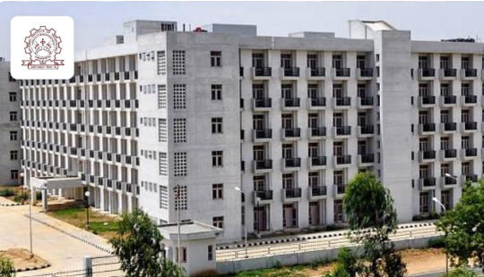
National Institute of Technology
Established in 1963 as a Regional Engineering College, NIT Kurukshetra was conferred the status of an Institute of National Importance in 2008. Located in the historic city of Kurukshetra, Haryana, approximately 160 km from Delhi, the institute offers a serene and conducive environment for academic and personal growth.
Academic Programs
NIT Kurukshetra offers a diverse range of undergraduate, postgraduate, and doctoral programs:
Undergraduate (B.Tech): Civil, Computer Science, Electrical, Electronics & Communication, Mechanical, Industrial Engineering & Management, Information Technology, Artificial Intelligence & Machine Learning, and Mathematics & Computing.
Postgraduate (M.Tech): Specializations in Structural Engineering, Power Systems, VLSI Design, Thermal Engineering, and more.
MBA: Specializations in Marketing, Finance, Human Resource Management, and Information Technology.
MCA: Master of Computer Applications.
Ph.D.: Offered in various disciplines across Engineering, Sciences, and Humanities.
Admissions
B.Tech: Admission is based on the Joint Entrance Examination (JEE) Main scores, followed by JoSAA counseling. Eligibility requires a minimum of 75% aggregate marks in Class 12 with Physics, Chemistry, and mathematics.
M.Tech: Admission is through the Graduate Aptitude Test in Engineering (GATE) scores. Non-GATE candidates may be considered based on academic performance.
MBA: Admission is based on CAT or JMET scores, followed by Group Discussion and Personal Interview.
MCA: Admission is through the National Institute of Technology MCA Common Entrance Test (NIMCET).
Ph.D.: Admission is through an institute-specific entrance test and interview.
Campus and Infrastructure
NIT Kurukshetra's campus is organized into three functional sectors: instructional buildings, hostels, and residential areas for staff. The infrastructure includes:
Library: A spacious library with over 100,000 books, 6,028 back volumes, and 2,800+ online journals.
Centre of Computing and Networking (CCN): A centralized facility providing 24/7 internet access, email services, and online test infrastructure.
Senate Hall: A state-of-the-art conference-cum-canteen facility for seminars and workshops.
Sports Complex: Facilities for basketball, volleyball, lawn tennis, badminton, racquetball, cricket, football, and a 400m athletic track.
Hostels: 12 hostels (9 for boys and 3 for girls) equipped with modern amenities.
Health Centre: Provides OPD services, dental care, laboratory tests, pharmacy, and emergency services.
Placements
The Training and Placement Cell at NIT Kurukshetra facilitates internships and placements for students. In the 2024 placement session:
B.Tech: 590 students placed with an average package of ₹12.68 LPA and the highest package of ₹64.28 LPA.
M.Tech: 197 students placed with an average package of ₹11.19 LPA.
MBA: Offers placements with packages ranging from ₹3 LPA to ₹38.87 LPA.
Top recruiters include Infosys, TCS, Wipro, Google, Amazon, Flipkart, and others.
Research and Innovation
NIT Kurukshetra is actively involved in research projects funded by DST, MHRD, CSIR, AICTE, and UGC. The institute focuses on emerging areas such as artificial intelligence, renewable energy, and sustainable development. Collaborations with industries and academic institutions enhance research output and innovation.
Rankings
As per the National Institutional Ranking Framework (NIRF) 2024, NIT Kurukshetra is ranked 81st among engineering institutions in India.
Conclusion
National Institute of Technology Kurukshetra stands as a premier institution offering quality education, robust infrastructure, and excellent placement opportunities. With a focus on research, innovation, and industry collaboration, it prepares students to meet global challenges and contribute to technological advancements. The institute's commitment to excellence makes it a preferred choice for aspiring engineers and technologists.
1 note
·
View note
Text
Career Prospects in ECE in Hyderabad and How HITAM Prepares Students for Success

Electronics and Communication Engineering (ECE) is a dynamic and evolving branch of engineering that plays a crucial role in today’s technology-driven world. With the expansion of communication networks, the Internet of Things (IoT), embedded systems, and smart devices, the field of ECE has become a highly sought-after domain among students and industries alike. If you’re based in Hyderabad or looking to pursue ECE in this region, you're in a hotspot of academic excellence and thriving tech industries.
Let’s explore the scope of Electronics and Communication Engineering in Hyderabad, what you should look for in a college, and how HITAM (Hyderabad Institute of Technology and Management) stands out in equipping students with the skills and knowledge to thrive in this field.
Why Choose Electronics and Communication Engineering?
ECE is a broad and versatile field that combines two major domains: electronics (hardware) and communication (including networks and signal processing). It deals with the design, development, and application of devices, circuits, and communication equipment such as transmitters, receivers, and integrated circuits.
Some key areas of ECE include:
- Embedded Systems
- VLSI Design
- IoT and Robotics
- Signal Processing
- Wireless Communication
- Satellite and Optical Communication
- Networking and Cybersecurity
This diversity means ECE graduates can venture into core industries, IT sectors, research roles, and even managerial or entrepreneurial paths.
ECE in Hyderabad: A Thriving Opportunity
Hyderabad is a leading hub for IT and electronics in India. With the presence of tech giants such as Microsoft, Qualcomm, Intel, and numerous research organizations, there is a consistent demand for skilled ECE professionals. Add to that the city’s robust infrastructure, start-up ecosystem, and academic excellence, and you’ve got a great environment for growth.
The top advantages of pursuing Electronics and Communication Engineering in Hyderabad include the following:
1) Proximity to leading industries: Students have the chance to intern, train, and work with companies in both core electronics and IT services.
2) Academic collaborations: Reputed institutions in Hyderabad have collaborations with research bodies and industries that enhance the relevance of their curriculum.
3) Startup and innovation culture: T-Hub and other innovation centers in Hyderabad promote entrepreneurship, which is ideal for ECE students inclined toward innovation.
4) Access to Research: ECE students can participate in advanced research on topics like wireless networks, nanotechnology, and IoT through institutional programs.
How HITAM Stands Out in ECE Education
The Hyderabad Institute of Technology and Management (HITAM) offers a comprehensive B.Tech program in Electronics and Communication Engineering designed to prepare students for real-world challenges.
1) Industry-Aligned Curriculum: HITAM’s curriculum goes beyond textbooks. It integrates practical knowledge through project-based learning, industry case studies, and workshops. Subjects are updated based on the evolving trends in AI, IoT, embedded systems, and 5G communication.
2) Strong Focus on Innovation and Research: HITAM encourages students to take up interdisciplinary projects from early semesters. Their innovation centers and labs are equipped to support research in VLSI, communication systems, and signal processing.
3) Skill Development Programs: The institution partners with industry leaders for certification programs and technical training. This helps bridge the gap between theoretical learning and practical application, making HITAM students job-ready.
4) Experienced Faculty: The ECE department at HITAM has a team of dedicated and highly qualified faculty members who mentor students academically and professionally.
5) Entrepreneurship and Leadership: HITAM supports entrepreneurial initiatives among students through innovation cells and startup incubation support. The institution promotes a mindset of leadership and innovation.
6) Placement Opportunities: HITAM boasts a strong placement record with reputed recruiters from core sectors, IT companies, and public sector undertakings. Their training and placement cell regularly conducts soft skills training sessions, coding workshops, and mock interviews.
Career Opportunities After ECE from HITAM
Graduates from HITAM’s ECE program have multiple career paths:
Core Electronics Jobs: Circuit design, embedded systems, PCB design, control systems
Communication and Networking: RF engineering, network administration, telecom services
IT and Software: Software development, data science, machine learning
Government and PSUs: Indian Engineering Services (IES), DRDO, ISRO, BHEL, BEL
Higher Studies & Research: M.Tech/MS in India or abroad, Ph.D. opportunities
Entrepreneurship: Developing tech startups in IoT, robotics, or automation
Conclusion
Choosing Electronics and Communication Engineering in Hyderabad is a wise decision, given the city’s robust technological ecosystem and excellent educational infrastructure. Among the top institutes, HITAM stands out for its focus on innovation, industry integration, and holistic student development.
Whether you're passionate about building next-generation communication systems, diving into embedded technologies, or leading tech innovations, ECE at HITAM provides the platform you need to achieve your goals.
If you're exploring engineering options and want a future-ready, hands-on education in Electrical and Computer Engineering (ECE), HITAM is a worthy consideration.
Feel free to ask more if you'd like a breakdown of the course structure or student testimonials from HITAM’s ECE department.
0 notes
Text
Boost Your VLSI Career with the Best Training Institutes in Bangalore
The Rising Demand for VLSI Professionals With the exponential growth of the semiconductor industry, VLSI (Very Large Scale Integration) design has emerged as one of the most in-demand fields in electronics and embedded systems. From smartphones and computers to self-driving cars and smart appliances, VLSI technology plays a crucial role in enabling intelligent digital systems. Due to the increasing dependency on integrated circuits in almost every electronic device, there is a rising need for skilled VLSI professionals. This demand has led many aspiring engineers to seek quality training from reputed institutes in Bangalore, India’s hub for technology and innovation.
Why Bangalore is the Preferred Destination for VLSI Training Bangalore, often called the Silicon Valley of India, is home to numerous semiconductor companies, design houses, and electronics manufacturing firms. This environment creates ample opportunities for practical exposure and industry collaboration. Among the top vlsi institutes in bangalore, candidates can find a range of training programs that combine theoretical knowledge with hands-on lab experience. These institutes offer specialized courses in areas like digital design, physical design, ASIC verification, and FPGA implementation, catering to the evolving needs of the industry. Choosing the right institute in Bangalore gives learners a valuable edge in both knowledge and employment prospects.
Features of an Effective VLSI Training Program An ideal VLSI training program is structured to provide not only strong foundational concepts but also practical exposure using real-time tools and industry-standard software. Courses designed in alignment with current job roles help learners understand design flows, verification methodologies, and layout processes. Instructors with industry experience and the availability of live projects further enhance the learning experience. Institutes that offer placement support, interview preparation, and resume guidance are often preferred by candidates aiming for a stable career in VLSI.
The Role of VLSI Training in Career Advancement Fresh graduates and working professionals who wish to enter the semiconductor domain can significantly benefit from VLSI training. These programs are crafted to develop technical proficiency and make learners job-ready. Bangalore provides a dynamic setting where individuals can access the latest tools, interact with domain experts, and build a professional network. A focused VLSI training program in this city can open the door to numerous job opportunities in top semiconductor firms.
Choosing a Job-Oriented VLSI Institute Enrolling in a job oriented vlsi training institute in bangalore can be a game-changer for anyone aiming to enter the core electronics field. Such institutes focus on equipping students with industry-relevant skills and practical expertise, thus improving their employability. These job-oriented programs emphasize real-world applications, timely projects, and guidance that align with current hiring trends in the VLSI sector.
Conclusion VLSI is a promising field with ever-expanding opportunities. For aspiring engineers looking to start or grow their careers in this domain, choosing the right training institute is critical. Bangalore stands out as a prime destination due to its strong industry presence and top-quality education providers. One of the most trusted names in this space is Takshila Institute of VLSI Technologies, known for offering robust, industry-aligned training. From comprehensive curriculum to placement support, the right institute can significantly impact an individual's career path. In conclusion, selecting the best institute from the top vlsi institutes in bangalore or opting for a job oriented vlsi training institute in bangalore can be the key step toward a successful future in the semiconductor industry.
0 notes
Text
Unlocking Future Tech Careers: VLSI Design and Verification Training in Demand
The Rising Importance of VLSI in Modern Technology
In a world dominated by digital devices, the demand for skilled professionals in the semiconductor industry is steadily increasing. From smartphones and laptops to automotive systems and healthcare devices, complex integrated circuits power everyday technologies. At the core of this advancement lies VLSI (Very-Large-Scale Integration), a specialization that enables the design of microchips containing millions of transistors. With industries investing in chip design more than ever, VLSI professionals with advanced technical knowledge are highly sought after.
Why RTL Verification is Crucial in Semiconductor Design
One of the most essential aspects of chip design is ensuring that the digital circuits behave as expected. This is where rtl verification training in hyderabad plays a critical role. RTL (Register Transfer Level) verification involves checking the functionality and logic of digital designs before they proceed to fabrication. For students and engineers in Hyderabad—a city known for its growing tech ecosystem—getting trained in RTL verification opens up promising career opportunities. Hands-on training programs not only improve understanding of verification concepts but also offer practical exposure to simulation tools and methodologies used in the industry.
The Industry's Growing Focus on Skilled VLSI Talent
Technology companies today are looking for engineers who are not only theoretically sound but also industry-ready. Academic learning often lacks exposure to the challenges and tools used in real-time chip design environments. To bridge this gap, many professionals are turning to specialized training courses that focus on applied learning. Such programs help in understanding not just how chips are designed but also how errors are detected and corrected efficiently before production.
How Specialized Courses Prepare for Real-World Applications
VLSI training institutes are now integrating real-world projects and industry case studies into their programs. These modules focus on areas such as digital design, verification, static timing analysis, and synthesis. By simulating the work environment of semiconductor companies, these training modules allow learners to adapt to workplace challenges even before joining the industry. This hands-on experience boosts both technical and problem-solving skills, essential for long-term career growth.
Choosing the Right Advanced Course for Career Advancement
For those looking to excel in chip design and verification, enrolling in an advanced vlsi design and verification course can be a game-changer. These programs cover the entire design flow from RTL coding to functional verification, ensuring a comprehensive understanding of the VLSI domain. Particularly for job-seekers and engineering graduates, such training improves employability by aligning academic skills with current industry requirements.
Conclusion
As the semiconductor industry continues to expand, so does the need for professionals with expertise in design and verification. The role of targeted learning through rtl verification training in hyderabad and an advanced vlsi design and verification course cannot be overstated. These programs enable learners to confidently step into a competitive job market equipped with the right knowledge and tools. Institutions like takshila-vlsi.com are helping meet this demand by offering detailed and practical training experiences. In conclusion, gaining specialized skills in VLSI can lead to long-term career stability and growth in a rapidly evolving tech-driven world.
0 notes