#VHDL design flow
Explore tagged Tumblr posts
Visit Tumblr Blog
Explore Tumblr blogs with no restrictions, modern design and the best experience.
Last Seen Tumblr Blogs


Fun Fact
The total number of visits Tumblr.com received during January 2021 is 327 million.
Text
Understanding FPGA Architecture: Key Insights
Introduction to FPGA Architecture
Imagine having a circuit board that you could rewire and reconfigure as many times as you want. This adaptability is exactly what FPGAs offer. The world of electronics often seems complex and intimidating, but understanding FPGA architecture is simpler than you think. Let’s break it down step by step, making it easy for anyone to grasp the key concepts.
What Is an FPGA?
An FPGA, or Field Programmable Gate Array, is a type of integrated circuit that allows users to configure its hardware after manufacturing. Unlike traditional microcontrollers or processors that have fixed functionalities, FPGAs are highly flexible. You can think of them as a blank canvas for electrical circuits, ready to be customized according to your specific needs.
How FPGAs Are Different from CPUs and GPUs
You might wonder how FPGAs compare to CPUs or GPUs, which are more common in everyday devices like computers and gaming consoles. While CPUs are designed to handle general-purpose tasks and GPUs excel at parallel processing, FPGAs stand out because of their configurability. They don’t run pre-defined instructions like CPUs; instead, you configure the hardware directly to perform tasks efficiently.
Basic Building Blocks of an FPGA
To understand how an FPGA works, it’s important to know its basic components. FPGAs are made up of:
Programmable Logic Blocks (PLBs): These are the “brains” of the FPGA, where the logic functions are implemented.
Interconnects: These are the wires that connect the logic blocks.
Input/Output (I/O) blocks: These allow the FPGA to communicate with external devices.
These elements work together to create a flexible platform that can be customized for various applications.
Understanding Programmable Logic Blocks (PLBs)
The heart of an FPGA lies in its programmable logic blocks. These blocks contain the resources needed to implement logic functions, which are essentially the basic operations of any electronic circuit. In an FPGA, PLBs are programmed using hardware description languages (HDLs) like VHDL or Verilog, enabling users to specify how the FPGA should behave for their particular application.
What are Look-Up Tables (LUTs)?
Look-Up Tables (LUTs) are a critical component of the PLBs. Think of them as small memory units that can store predefined outputs for different input combinations. LUTs enable FPGAs to quickly execute logic operations by “looking up” the result of a computation rather than calculating it in real-time. This speeds up performance, making FPGAs efficient at performing complex tasks.
The Role of Flip-Flops in FPGA Architecture
Flip-flops are another essential building block within FPGAs. They are used for storing individual bits of data, which is crucial in sequential logic circuits. By storing and holding values, flip-flops help the FPGA maintain states and execute tasks in a particular order.
Routing and Interconnects: The Backbone of FPGAs
Routing and interconnects within an FPGA are akin to the nervous system in a human body, transmitting signals between different logic blocks. Without this network of connections, the logic blocks would be isolated and unable to communicate, making the FPGA useless. Routing ensures that signals flow correctly from one part of the FPGA to another, enabling the chip to perform coordinated functions.
Why are FPGAs So Versatile?
One of the standout features of FPGAs is their versatility. Whether you're building a 5G communication system, an advanced AI model, or a simple motor controller, an FPGA can be tailored to meet the exact requirements of your application. This versatility stems from the fact that FPGAs can be reprogrammed even after they are deployed, unlike traditional chips that are designed for one specific task.
FPGA Configuration: How Does It Work?
FPGAs are configured through a process called “programming” or “configuration.” This is typically done using a hardware description language like Verilog or VHDL, which allows engineers to specify the desired behavior of the FPGA. Once programmed, the FPGA configures its internal circuitry to match the logic defined in the code, essentially creating a custom-built processor for that particular application.
Real-World Applications of FPGAs
FPGAs are used in a wide range of industries, including:
Telecommunications: FPGAs play a crucial role in 5G networks, enabling fast data processing and efficient signal transmission.
Automotive: In modern vehicles, FPGAs are used for advanced driver assistance systems (ADAS), real-time image processing, and autonomous driving technologies.
Consumer Electronics: From smart TVs to gaming consoles, FPGAs are used to optimize performance in various devices.
Healthcare: Medical devices, such as MRI machines, use FPGAs for real-time image processing and data analysis.
FPGAs vs. ASICs: What’s the Difference?
FPGAs and ASICs (Application-Specific Integrated Circuits) are often compared because they both offer customizable hardware solutions. The key difference is that ASICs are custom-built for a specific task and cannot be reprogrammed after they are manufactured. FPGAs, on the other hand, offer the flexibility of being reconfigurable, making them a more versatile option for many applications.
Benefits of Using FPGAs
There are several benefits to using FPGAs, including:
Flexibility: FPGAs can be reprogrammed even after deployment, making them ideal for applications that may evolve over time.
Parallel Processing: FPGAs excel at performing multiple tasks simultaneously, making them faster for certain operations than CPUs or GPUs.
Customization: FPGAs allow for highly customized solutions, tailored to the specific needs of a project.
Challenges in FPGA Design
While FPGAs offer many advantages, they also come with some challenges:
Complexity: Designing an FPGA requires specialized knowledge of hardware description languages and digital logic.
Cost: FPGAs can be more expensive than traditional microprocessors, especially for small-scale applications.
Power Consumption: FPGAs can consume more power compared to ASICs, especially in high-performance applications.
Conclusion
Understanding FPGA architecture is crucial for anyone interested in modern electronics. These devices provide unmatched flexibility and performance in a variety of industries, from telecommunications to healthcare. Whether you're a tech enthusiast or someone looking to learn more about cutting-edge technology, FPGAs offer a fascinating glimpse into the future of computing.
2 notes
·
View notes
Text
Mastering VLSI: Why the Right Training Matters for a Thriving Tech Career
The Rising Demand for VLSI Experts The modern world is driven by electronics. From smartphones to smart cars, every innovation depends on microchips designed using VLSI (Very Large Scale Integration) technology. With the growing use of AI, IoT, and automation, the need for skilled VLSI professionals has increased rapidly. This makes VLSI an essential field for those looking to build a strong career in electronics and semiconductor industries. Choosing the right learning path is key to making the most of this opportunity.
Exploring the Benefits of VLSI Online Training Courses Many learners today seek flexible and effective ways to upskill. VLSI online training courses offer an excellent solution by combining convenience with quality education. These courses provide access to experienced instructors, practical assignments, and industry-based projects—all from the comfort of home. Learners can grasp digital design, physical design, verification, and ASIC/FPGA concepts without sacrificing their job or academic responsibilities. The online model also allows repeated learning and flexible scheduling, making it ideal for beginners as well as professionals wanting to upgrade their knowledge.
Choosing the Right Learning Mode While online learning provides flexibility, some individuals prefer classroom-based teaching for real-time interaction and immediate doubt clearing. The choice between online and offline modes largely depends on individual preferences, learning habits, and career goals. However, what truly matters is the quality of the training and the expertise of the instructors involved.
Key Skills Taught in VLSI Training A well-structured VLSI course should cover areas like CMOS technology, HDL languages such as Verilog and VHDL, physical design flow, and functional verification techniques. Practical exposure through lab sessions or simulation tools is crucial. Additionally, learners should be guided on real-time projects to apply their theoretical knowledge to industry problems.
Why VLSI Coaching in Hyderabad is Gaining Popularity Hyderabad has become a major hub for semiconductor and electronics industries. As a result, VLSI coaching in Hyderabad has gained recognition for producing skilled professionals. Reputed training centers in the city offer tailored coaching with an industry-aligned curriculum, experienced faculty, and placement support. Many aspirants from across the country travel to Hyderabad to benefit from this coaching environment that bridges academic learning with industry demands.
Conclusion VLSI technology plays a vital role in shaping the electronics and semiconductor industries. Whether through VLSI online training courses or classroom-based programs like VLSI coaching in Hyderabad, acquiring the right skills is essential for career growth. Institutions like Takshila Institute of VLSI Technologies provide training that matches industry standards, helping learners succeed in a competitive field. The choice of platform and location may differ, but the goal remains the same—building a strong foundation in VLSI for a successful future.
0 notes
Text
Advance Your Career with RTL Verification Training at Takshila Institute of VLSI Technologies
RTL (Register Transfer Level) Verification is a fundamental process in the VLSI design flow. It involves checking the logic and functionality of a digital circuit design described in a hardware description language such as Verilog or VHDL. The goal is to ensure the design behaves as intended before it moves to synthesis and physical implementation. RTL verification includes writing testbenches, performing simulation, and applying assertions and coverage metrics to validate the design thoroughly. As VLSI designs grow in complexity, efficient RTL verification becomes essential to catch logical bugs early in the design cycle, saving time and cost.
Importance of RTL Verification Training
With the increasing demand for faster and more reliable chips, companies are investing heavily in design verification. As a result, RTL verification engineers are among the most sought-after professionals in the semiconductor industry. However, becoming a proficient verification engineer requires deep knowledge of digital design, verification methodologies like UVM (Universal Verification Methodology), and hands-on experience with simulation tools. This is where structured training plays a crucial role. High-quality RTL verification training helps learners bridge the gap between academic theory and industry practice.
A Leading Training Institute in Hyderabad
For those seeking specialized RTL verification training in Hyderabad, the Takshila Institute of VLSI Technologies is a trusted name in India. The institute is renowned for its focused curriculum, experienced trainers, and strong industry connections. Takshila's RTL verification program is carefully designed to meet current industry standards, incorporating both theoretical concepts and hands-on lab sessions.
The training includes modules on SystemVerilog, functional simulation, UVM-based environments, and testbench development. Participants also get exposure to real-time projects and debugging techniques using industry-standard tools. The institute ensures that students develop a strong foundation and are job-ready upon course completion.
Why Choose Takshila Institute in Hyderabad?
Among RTL verification training institutes, Takshila Institute of VLSI Technologies in Hyderabad stands out due to its quality of instruction, practical learning approach, and placement support. The institute not only trains students in technical skills but also prepares them for interviews and real-world challenges through mock tests and industry interaction sessions.
With a consistent track record of successful placements in leading semiconductor companies, Takshila is the ideal destination for aspiring RTL verification engineers. Whether you are a fresh graduate or a working professional aiming to shift into VLSI, this institute provides the right guidance and support to help you succeed.
0 notes
Text
What is VLSI Design and Communication Systems? A Comprehensive Guide
Introduction In today’s tech-driven world, VLSI design and communication systems power modern electronics and connectivity. Let’s simplify their importance!
What is VLSI Design? VLSI (Very Large Scale Integration) involves designing integrated circuits (ICs) with millions of transistors on a single chip. It’s the core of devices like smartphones and computers.
Evolution of VLSI From bulky circuits with few transistors to compact, efficient chips, VLSI has revolutionized modern electronics by making devices smaller, faster, and smarter.
Key Elements of VLSI Design
Logic Design: Creates circuits for logical operations using languages like VHDL or Verilog.
Physical Design: Lays out transistors and components to optimize performance.
Verification: Ensures the design works flawlessly before production.
Communication Systems: The Backbone of Connectivity Communication systems enable information flow between devices, from mobile phones to satellites.
Components of Communication Systems
Transmitter: Converts data into signals for transmission.
Channel: The medium (fiber optics or airwaves) carrying the signals.
Receiver: Captures and converts signals into usable forms.
Types of Communication Systems
Analog: Continuous signals (e.g., landline phones).
Digital: Faster, secure data transmission in bits (e.g., Internet, mobile networks).
VLSI and Communication Systems: The Perfect Duo
Chip Design: VLSI enables high-speed, low-power chips for communication devices.
Signal Processing: VLSI processes signals for reliable, fast communication.
Challenges
Power Consumption: Designing energy-efficient chips is tough.
Signal Interference: Ensuring quality signals in wireless systems.
Scaling Limits: Miniaturizing transistors faces material and performance barriers.
Conclusion VLSI design creates ultra-compact, powerful chips, while communication systems enable seamless information flow. Together, they power modern technology, from smartphones to IoT, shaping the future of connectivity and innovation.
https://kce.ac.in/what-is-vlsi-design-and-communication-systems-a-comprehensive-guide/
0 notes
Text
VLSI Design And Verification Course For Fresher - VLSI Guru
In the fast-paced world of technology, the VLSI (Very Large Scale Integration) domain stands as a cornerstone for innovations in electronics and semiconductor design. If you’re a fresher aiming to dive into this exciting field, the VLSI Design and Verification Course by VLSI Guru is your perfect launchpad.

Why Choose VLSI as a Career Path?
The demand for skilled professionals in VLSI design and verification is skyrocketing, with industries relying on advanced ASIC (Application-Specific Integrated Circuits) and FPGA (Field-Programmable Gate Arrays) to power cutting-edge technologies. From smartphones to autonomous vehicles, the scope of VLSI is vast and evolving.
What Does the Course Offer?
The VLSI Design and Verification Course by VLSI Guru is tailored for freshers, focusing on:
HDL Languages: Master Verilog and VHDL for RTL coding.
SystemVerilog & UVM: Learn modern verification methodologies for building robust testbenches.
ASIC Design Flow: Gain insights into the complete chip design process.
FPGA Prototyping: Get hands-on experience with FPGA tools and workflows.
Debugging & Tools Expertise: Work with industry-standard tools like Cadence, Synopsys, and Mentor Graphics.
Why VLSI Guru?
VLSI Guru emphasizes practical learning through real-world projects and labs. Freshers are trained to handle challenges in semiconductor design and verification, bridging the gap between academia and industry.
Who Can Enroll?
The course is ideal for engineering graduates in ECE, EE, or CSE with a passion for chip design and a desire to work in leading semiconductor companies.
Start your journey in the semiconductor industry today with VLSI Guru's specialized training.
0 notes
Text
AMD Vivado Design Suite 2024.2: Versal SoCs Revolutionized

What Is AMD Vivado?
A collection of design tools for AMD adaptive SoCs and FPGAs is called AMD Vivado. It contains tools for place and route, design entry, synthesis, verification, and simulation.
AMD Vivado Design Suite
The 2024.2 version, which includes significant improvements for designing with AMD Versal adaptable SoCs, is now available.
AMD Vivado 2024.2 highlights
Improved Versal Adaptive SoC Design Flows for AMD.
Fast Place and Route for All Versal Devices
Improved Advanced Flow for Quick Compilation.
Routability and congestion optimization.
Enabling Top-Level RTL Flows
Makes it possible to use transceivers from the top-level RTL and Versal programmable network on chip (NoC).
Fast Boot of Processing System in Versal Devices
Segmented setup for quick OS.
Startup that satisfies a range of boot-sequence needs.
Facilitating quicker design iterations and achieving your FMAX goals more rapidly
The design program for AMD adaptive SoCs and FPGAs is called AMD Vivado. Design Entry, Synthesis, Place and Route, and Verification/Simulation tools are among its components.
Discover how sophisticated capabilities in the Vivado design tools enable designers to more precisely estimate power for AMD adaptive SoCs and FPGAs while cutting down on compilation times and design cycles.
Benefits
AMD Vivado Meeting Fmax Targets
One of the most difficult stages of the hardware design cycle is reaching your FMAX objective in a high-speed design. Vivado has special capabilities that assist you close timing, such Intelligent Design Runs (IDR), Report QoR Assessment (RQA), and Report QoR Suggestions (RQS). By using RQA, RQS, and IDR, you may reach your performance targets in a matter of days rather than weeks, which will increase your productivity significantly.
AMD Vivado Faster Design Iterations
As developers troubleshoot their ideas and add new features, design iterations are typical. These iterations are frequently minor adjustments made to a tiny section of the design. Incremental compile and Abstract Shell are two essential technologies in the AMD Vivado Design Suite that drastically cut down on design iteration times.
AMD Power Design Manager
Early and precise power prediction is essential for informing important design choices when creating FPGA and adaptive SoCs. For big and complicated devices like the Versal and UltraScale+ families, Power Design Manager is a next-generation power estimating tool designed to enable precise power estimation early in the design process. This tool was created especially to give precise power estimates for devices that have a lot of complicated hard IP blocks.
Design Flows
Design Entry & Implementation
Design entry in conventional HDL, such as VHDL and Verilog, is supported by AMD Vivado. Additionally, it supports the IP Integrator (IPI), a graphical user interface-based tool that enables a Plug-and-Play IP Integration Design Environment.
For today’s sophisticated FPGAs and SOCs, Vivado offers the finest synthesis and implementation available, with integrated timing closure and methodology capabilities.
Users may confine their design, assess findings, and close timing with the aid of the UltraFast methodology report (report_methodology), which is accessible in Vivado’s default flow.
Verification and Debug
To guarantee the final FPGA implementation’s functionality, performance, and dependability, verification and hardware debugging are essential. Effective validation of design functionality is made possible by the verification elements of the Vivado tool. Its extensive debugging capabilities enable engineers to quickly identify and fix problems in intricate designs.
Dynamic Function eXchange
With Dynamic Function eXchange (DFX), designers may make real-time changes to specific parts of their designs. The remaining logic can continue to function as designers download partial bitstreams to their AMD devices. This creates a plethora of opportunities for real-time performance improvements and design modifications. Designers may cut power consumption, upgrade systems in real-time, and switch to fewer or smaller devices via Dynamic Function eXchange.
AMD Vivado Platform Editions
AMD Vivado Design Suite- Standard & Enterprise Editions
AMD Vivado Design Suite Standard Edition is available for free download. The Enterprise Edition’s license options start at $2,995.
Features
Licensing Options
AMD Vivado Standard
You may download the AMD Vivado Standard Edition for free, giving you immediate access to its essential features and capabilities.
AMD Vivado Enterprise
All AMD devices are supported by the fully functional Vivado Enterprise Edition of the design suite.
Recommended System Memory
Each target device family’s average and maximum AMD Vivado Design Suite memory utilization. AMD advises allocating enough physical memory to handle periods of high consumption.
Remarks
The more LUT and CLB are used, the more memory is used. The following figures were calculated with an average LUT usage of around 75%.
The amount of memory used is strongly impacted by the magnitude and complexity of timing restrictions.
The following figures were produced on a single synthesis and implementation run using the AMD Vivado tools in programmed batch mode.
DFX flow may result in increased memory use.
These devices are not compatible with 32-bit computers.
Answer Record 14932 describes how to set up a Windows 32-bit computer to use 3 GB of RAM.
Operation System
The following operating systems are compatible with AMD’s x86 and x86-64 chip architectures.
Features
Support for Microsoft Windows.
10.0 1809, 1903, 1909, and 2004 are Windows updates.
Support for Linux.
7.4, 7.5, 7.6, 7.7, 7.8, and 7.9 for CentOS and RHEL 7.
CentOS/RHEL 8: 8.1, 8.2, 8.3.
LE SUSE: 12.4, 15.2.
Among Ubuntu’s LTS versions are 16.04.5, 16.04.6, 18.04.1, 18.04.2, and 18.04.3, 18.04.4 LTS, 20.04 LTS, and 20.04.1 LTS.
Read more on Govindhtech.com
#AMDVivado#VivadoDesignSuite#Versal#VersalSoCs#FPGAs#DesignSuite#News#Technews#Technology#Technologynews#Technologytrends#Govindhtech
0 notes
Text
Understanding FPGA Architecture: Key Insights
Introduction to FPGA Architecture
Imagine having a circuit board that you could rewire and reconfigure as many times as you want. This adaptability is exactly what FPGAs offer. The world of electronics often seems complex and intimidating, but understanding FPGA architecture is simpler than you think. Let’s break it down step by step, making it easy for anyone to grasp the key concepts.
What Is an FPGA?
An FPGA, or Field Programmable Gate Array, is a type of integrated circuit that allows users to configure its hardware after manufacturing. Unlike traditional microcontrollers or processors that have fixed functionalities, FPGAs are highly flexible. You can think of them as a blank canvas for electrical circuits, ready to be customized according to your specific needs.
How FPGAs Are Different from CPUs and GPUs
You might wonder how FPGAs compare to CPUs or GPUs, which are more common in everyday devices like computers and gaming consoles. While CPUs are designed to handle general-purpose tasks and GPUs excel at parallel processing, FPGAs stand out because of their configurability. They don’t run pre-defined instructions like CPUs; instead, you configure the hardware directly to perform tasks efficiently.
Basic Building Blocks of an FPGA
To understand how an FPGA works, it’s important to know its basic components. FPGAs are made up of:
Programmable Logic Blocks (PLBs): These are the “brains” of the FPGA, where the logic functions are implemented.
Interconnects: These are the wires that connect the logic blocks.
Input/Output (I/O) blocks: These allow the FPGA to communicate with external devices.
These elements work together to create a flexible platform that can be customized for various applications.
Understanding Programmable Logic Blocks (PLBs)
The heart of an FPGA lies in its programmable logic blocks. These blocks contain the resources needed to implement logic functions, which are essentially the basic operations of any electronic circuit. In an FPGA, PLBs are programmed using hardware description languages (HDLs) like VHDL or Verilog, enabling users to specify how the FPGA should behave for their particular application.
What are Look-Up Tables (LUTs)?
Look-Up Tables (LUTs) are a critical component of the PLBs. Think of them as small memory units that can store predefined outputs for different input combinations. LUTs enable FPGAs to quickly execute logic operations by “looking up” the result of a computation rather than calculating it in real-time. This speeds up performance, making FPGAs efficient at performing complex tasks.
The Role of Flip-Flops in FPGA Architecture
Flip-flops are another essential building block within FPGAs. They are used for storing individual bits of data, which is crucial in sequential logic circuits. By storing and holding values, flip-flops help the FPGA maintain states and execute tasks in a particular order.
Routing and Interconnects: The Backbone of FPGAs
Routing and interconnects within an FPGA are akin to the nervous system in a human body, transmitting signals between different logic blocks. Without this network of connections, the logic blocks would be isolated and unable to communicate, making the FPGA useless. Routing ensures that signals flow correctly from one part of the FPGA to another, enabling the chip to perform coordinated functions.
Why are FPGAs So Versatile?
One of the standout features of FPGAs is their versatility. Whether you're building a 5G communication system, an advanced AI model, or a simple motor controller, an FPGA can be tailored to meet the exact requirements of your application. This versatility stems from the fact that FPGAs can be reprogrammed even after they are deployed, unlike traditional chips that are designed for one specific task.
FPGA Configuration: How Does It Work?
FPGAs are configured through a process called “programming” or “configuration.” This is typically done using a hardware description language like Verilog or VHDL, which allows engineers to specify the desired behavior of the FPGA. Once programmed, the FPGA configures its internal circuitry to match the logic defined in the code, essentially creating a custom-built processor for that particular application.
Real-World Applications of FPGAs
FPGAs are used in a wide range of industries, including:
Telecommunications: FPGAs play a crucial role in 5G networks, enabling fast data processing and efficient signal transmission.
Automotive: In modern vehicles, FPGAs are used for advanced driver assistance systems (ADAS), real-time image processing, and autonomous driving technologies.
Consumer Electronics: From smart TVs to gaming consoles, FPGAs are used to optimize performance in various devices.
Healthcare: Medical devices, such as MRI machines, use FPGAs for real-time image processing and data analysis.
FPGAs vs. ASICs: What’s the Difference?
FPGAs and ASICs (Application-Specific Integrated Circuits) are often compared because they both offer customizable hardware solutions. The key difference is that ASICs are custom-built for a specific task and cannot be reprogrammed after they are manufactured. FPGAs, on the other hand, offer the flexibility of being reconfigurable, making them a more versatile option for many applications.
Benefits of Using FPGAs
There are several benefits to using FPGAs, including:
Flexibility: FPGAs can be reprogrammed even after deployment, making them ideal for applications that may evolve over time.
Parallel Processing: FPGAs excel at performing multiple tasks simultaneously, making them faster for certain operations than CPUs or GPUs.
Customization: FPGAs allow for highly customized solutions, tailored to the specific needs of a project.
Challenges in FPGA Design
While FPGAs offer many advantages, they also come with some challenges:
Complexity: Designing an FPGA requires specialized knowledge of hardware description languages and digital logic.
Cost: FPGAs can be more expensive than traditional microprocessors, especially for small-scale applications.
Power Consumption: FPGAs can consume more power compared to ASICs, especially in high-performance applications.
Conclusion
Understanding FPGA architecture is crucial for anyone interested in modern electronics. These devices provide unmatched flexibility and performance in a variety of industries, from telecommunications to healthcare. Whether you're a tech enthusiast or someone looking to learn more about cutting-edge technology, FPGAs offer a fascinating glimpse into the future of computing.
0 notes
Text
NO.1 VLSI System Design in India
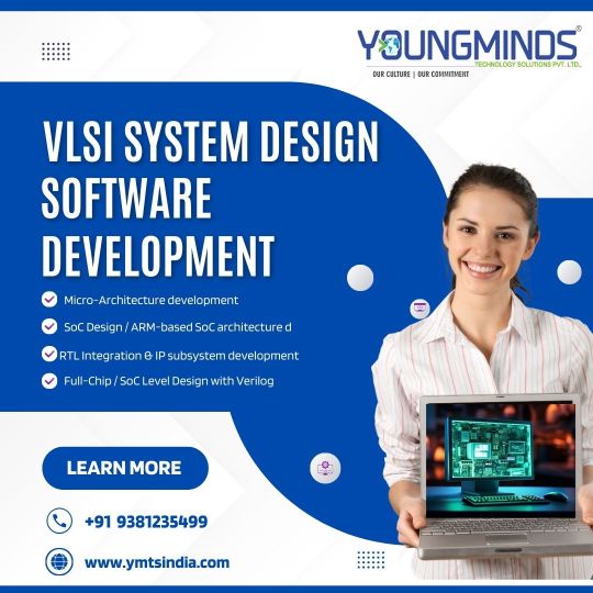
Welcome to Youngminds Technology Solutions, a leading VLSI System Design Software Development Agency in India. Our focus is on the development of the latest solutions that promote innovation and efficiency in the area of VLSI system design. Come with us as we are building the future of technology together.
Our VLSI design team has deep expertise in realizing product and software development for a wide range of application areas on cutting-edge technologies. YMTS team have wide set of skills across electronic chip design flow from specification to GDSII on latest node technologies, with special focus on RTL/FPGA Design, design verification and FPGA emulation.
VLSI SYSTEM DESIGN ASIC / FPGA Design Development
Design is not just what it looks like and feels like. Design is how it works.” You can hire us to build your custom website that fulfils your unique requirements. Unlike using a pre-built template for your site, a customized website is specifically created for you.
VLSI Services our Engineering team expertise in various stages of the design flow, Such as:
Micro-Architecture development for given specifications
SoC Design / ARM-based SoC architecture designs
RTL Integration & IP subsystem development
Full-Chip / SoC Level Design with Verilog, VHDL, System Verilog
Migration from FPGA to ASIC
Lint, CDC Checks and writing waivers
Integration of digital and analogue blocks (Like SERDES PMA + PCS or DDR + Phy etc.,)
Synthesis, STA Constraints for both ASIC and FPGA
Logic equivalency and formality checks
Hands-on experience on Various Industrial EDA tools
Optimization of Power, Area and timing trade off
FPGA Prototyping on Xilinx / Altera FPGA Boards
Optimization & Maintenance
We are here to help you understand the importance of web application maintenance. We provide several services which will enable your web application run error-free and smooth.
Our knowledge-based AI platform driven by automation and innovation. It enables our clients’ businesses to continuously reinvent system landscapes and achieve IT goals that align with business needs. By aligning IT with business value, we help clients push the envelope beyond cost and quality.
Training
YMTS provides training programs that help students / Engineers and customers get to productivity faster. All our training programs have been developed keeping in mind what it takes to accelerate skill development of today's R&D engineers and have been proven in-house with our own new hires as well as multiple customers.
As a top VLSI System Design Software Development Services, we are proud of the excellent services we offer. Our knowledge and dedication assure the best solutions for your VLSI requirements. Select us for the best performance in the VLSI system design. Visit More Information: https://ymtsindia.com/vlsi-system-design Meta Tags: VLSI System Design, VLSI System Management, VLSI Design Services, VLSI System Design Agency
0 notes
Text
5 Reasons for Using an Open Source Register Automation Tool | Agnisys
Register automation is an integral part of IP and SoC development. Long ago, design, verification, firmware, and documentation teams preferred doing register management manually or each team wrote their own scripts for limited automation. Later, companies started doing this automation at the organization level. Central scripts were written for register automation for design, verification, firmware, and documentation teams, but still each had their own specifications. This led to many iterations between these teams before different collaterals were all brought in sync. As design complexity grew, maintaining these scripts became difficult, and commercial EDA tools took their place. Simultaneously, many open source tools also cropped up that could be used for register automation. Although commercial tools have their own value proposition, open source tools also have their use cases. The five primary reasons why you might use open source tool are:
1. Cost
Open source EDA tools are typically free to use as there is no license fee, support fee, etc. You can just download, install, and get going. Generally, these tools are ideal for students, academicians, and perhaps small companies or cash-starved start-ups. If the cost to fix a bug in the final product developed using an open source tool is less than the cost of a commercial EDA tool for register automation, then it may be beneficial to opt for it.
For companies, there are a few more factors that affect the cost indirectly; experienced CAD engineers are required to integrate the tool in the production environment without any compatibility issues. Also, design and verification teams must be able to quickly ramp up on the tool to be able to churn out fully tested and verified designs faster in order to meet the shrinking market window. Some software engineers may also be needed to fix any issues or tailor the open source tool to meet unique requirements.
Considering all the above factors, if you can ensure that the total cost of ownership of an open source tool remains less, then the open source tool can turn out to be cost-effective for your organization.
If saving money on a commercial tool is more important than the money spent on finding bugs later in the development flow then you can perhaps go with the open source solutions.
2. Features
More options, more confusion! Fewer options, less confusion!
Generally, commercial EDA tools offer a comprehensive range of features and functionalities, including a rich set of special registers, a large number of properties for customization, etc. as they are developed and maintained by dedicated teams with extensive resources and customer interactions.
The open source tools may not support comprehensive features and functionality, but with fewer options you are not spoiled for choice. Assess the specific requirements of your project, including design complexity, input specification format (System RDL/IP-XACT/Excel/Document or a mix of these formats), required output collateral formats (Verilog, VHDL, System Verilog, UVM, HTML, PDF, Markdown, etc.), performance targets, and time-to-market constraints. Determine whether the features and capabilities of the open source tool align with these requirements.
With limited requirements you can be satisfied with a smaller set of features. For example, you may be using just one input specification format so you may not need a tool that supports a mix of formats. Similarly, you may require only design and verification collaterals, so why should you pay for other collaterals such as firmware, documentation, and custom outputs? Also, you may be working on FPGAs so ASIC related features could be of no use to you. You may be dealing with small and fairly simple designs so you may not require high performance features like clock-domain-crossing (CDC), functional safety, and so on. Working across teams and geography may not be important for you, rendering enterprise level features useless for you.
If you have simple register maps and don’t have any 3rd party IPs in IP-XACT and other formats, then open source may be enough for you.
3. DIY
Companies can start with the open-source software and set up a team of software engineers to modify the code for specific project requirements, tailoring the tools to fit the company's unique needs. The main challenge here is when updates of an open source software are released. It is usually a thrilling adventure into the unknown. Your engineering team may need to spend hours tinkering with config files and compiling the source to maintain compatibility with your production tool flow. Some previous features may suddenly disappear or be implemented differently as these tools are ever evolving. Merging your custom changes to open source code with new updates often requires a major and costly effort.
If hours spent tinkering with the output generation is not going to cause delay in the project and the cost of dedicating software engineers in developing, refining and maintaining the open source tool for several years is less than the cost of the commercial tools, then open source might be a possible solution.
4. Support
Many open-source projects have vibrant communities of users and developers who contribute to ongoing development, provide support, and share knowledge. While open source communities are there to help, you need to navigate through different forums for advice. Extensive documentation requires skills to extract the right information or else you can drown in the sea of available materials.
Support can be a weakness for open source tools. Troubleshooting is a costly affair, and often time consuming as well, delaying your critical project. There are no training programs, although there could be numerous tutorials available to help users learn the nitty gritty of the tools. This kind of community based approach to support can make troubleshooting a tedious task, affecting productivity, and risking your project success.
If time to market is not important for your project, then the absence of quick support may be acceptable.
5. Transparency, Scaling and Certification
With open source software, the code transparency can provide reassurance regarding security and reliability. Transparency may also expose vulnerabilities and critical flaws making these tools susceptible to attacks.
Open source tools also need to scale with your company’s evolving needs to support future innovation and competitiveness. Your company’s growth trajectory is linked to the evolution trajectory of the open source tool, which may be good enough for the short term but not suitable for long term strategy.
In certain industries, such as aerospace, automotive, and medical devices, regulatory compliance is critical. Companies making products in these domains do not have the luxury of using open source tools as they may not offer features and certifications to ensure compliance with industry standards and regulations.
Open source crowdsource development has its advantages but what happens when multiple users have conflicting requirements? One will always need a person to maintain the branch with their changes.
ISO 26262 certification requires that the tool vendor follows standard development processes to ensure tool quality, predictability, and fault management. If certification is not important or necessary then open source software can be used.
Conclusion
Open source register automation tools have their strengths and weaknesses. There are numerous use cases for these tools especially in academics, prototyping, and non-critical projects/products. However, many other industries and applications have requirements that can only be met with commercial register automation solutions. Open source tools may look cost-effective in the short term but, in the long term, the cost of ownership and the risk to the project outweighs the perceived benefits.
0 notes
Text
youtube
VHDL Basics : Begin the World of FPGA Design Tools & VHDL Design Flow
Welcome to our comprehensive guide on FPGA design tools and VHDL design flow! In this video, we dive into the fascinating world of FPGA design and explore the essential tools and methodologies needed for successful FPGA development. Whether you're a beginner or an experienced engineer, this tutorial will provide valuable insights and tips to enhance your FPGA design skills. We start by introducing the fundamentals of FPGA design, explaining the benefits and versatility of using FPGAs in various applications. From there, we explore the wide range of design tools available, from popular industry-standard software like Xilinx Vivado and Altera Quartus Prime to open-source alternatives like GHDL and Icarus Verilog. We highlight the strengths and features of each toolset, enabling you to choose the most suitable one for your projects. With a solid foundation in FPGA design and tools, we then delve into the VHDL (VHSIC Hardware Description Language) design flow. From understanding the basics of VHDL syntax to implementing complex digital designs, we provide step-by-step explanations and practical demonstrations. You'll learn about entity and architecture design, the importance of libraries, and how to simulate and synthesize VHDL code for your FPGA. To ensure a holistic learning experience, we discuss common challenges and pitfalls in FPGA design and provide valuable troubleshooting tips. We also touch upon advanced topics like FPGA optimization techniques, timing analysis, and physical implementation considerations. So, whether you're a student, hobbyist, or professional looking to enhance your FPGA design skills, this tutorial is the ultimate resource to get started on your journey. Join us now and unlock the vast potential of FPGA design tools and the VHDL design flow! FPGA design tools, VHDL design flow, FPGA development, Xilinx Vivado, Altera Quartus Prime, VHDL, Verilog, VHDL syntax, digital design, entity architecture, libraries, simulate VHDL code, synthesize VHDL code, FPGA optimization techniques, timing analysis, physical implementation, FPGA design skills.
Subscribe to "Learn And Grow Community"
YouTube : https://www.youtube.com/@LearnAndGrowCommunity
LinkedIn Group : https://www.linkedin.com/groups/7478922/
Blog : https://LearnAndGrowCommunity.blogspot.com/
Facebook : https://www.facebook.com/JoinLearnAndGrowCommunity/
Twitter Handle : https://twitter.com/LNG_Community
DailyMotion : https://www.dailymotion.com/LearnAndGrowCommunity
Instagram Handle : https://www.instagram.com/LearnAndGrowCommunity/
Follow #LearnAndGrowCommunity
#HDL Design#Digital Design#Verilog#VHDL#FPGA#Simulation#Synthesis#B.Tech#VLSI#Training#Career#ASIC#Xilinx#Students#hardware description language#VHDL tutorial#VHDL beginner guide#VHDL syntax#VHDL data types#VHDL modeling#behavioral modeling#data flow modeling#FSM#FPGA design tools#VHDL design flow#FPGA development#Xilinx Vivado#Altera Quartus Prime#entity#architecture
1 note
·
View note
Link
Digital Design: With an Introduction to the Verilog HDL, VHDL, and SystemVerilog 6th Edition, ISBN-13: 978-0134549897 [PDF eBook eTextbook] Publisher: Pearson; 6th edition (March 7, 2017) Language: English 720 pages ISBN-10: 9780134549897 ISBN-13: 978-0134549897 The speed, density, and complexity of today’s digital devices are made possible by advances in physical processing technology and digital design methodology. Aside from semiconductor technology, the design of leading-edge devices depends critically on hardware description languages (HDLs) and synthesis tools. Three public-domain languages, Verilog, VHDL, and SystemVerilog, all play a role in design flows for today’s digital devices. HDLs, together with fundamental knowledge of digital logic circuits, provide an entry point to the world of digital design for students majoring in computer science, computer engineering, and electrical engineering. In the not-too-distant past, it would be unthinkable for an electrical engineering student to graduate without having used an oscilloscope. Today, the needs of industry demand that undergraduate students become familiar with the use of at least one hardware description language. Their use of an HDL as a student will better prepare them to be productive members of a design team after they graduate. Given the presence of three HDLs in the design arena, we have expanded our presentation of HDLs in Digital Design to treat Verilog and VHDL, and to provide an introduction to SystemVerilog. Our intent is not to require students to learn three, or even two, languages, but to provide the instructor with a choice between Verilog and VHDL while teaching a systematic methodology for design, regardless of the language, and an optional introduction to SystemVerilog. Certainly, Verilog and VHDL are widely used and taught, dominate the design space, and have common underlying concepts supporting combinational and sequential logic design, and both are essential to the synthesis of high-density integrated circuits. Our text offers parallel tracks of presentation of both languages, but allows concentration on a single language. The level of treatment of Verilog and VHDL is essentially equal, without emphasizing one language over the other. A language-neutral presentation of digital design is a – common thread through the treatment of both languages. A large set of problems, which are stated in language-neutral terms, at the end of each chapter can be worked with either Verilog or VHDL. The emphasis in our presentation is on digital design, with HDLs in a supporting role. Consequently, we present only those details of Verilog, VHDL, and SystemVerilog that are needed to support our treatment of an introduction to digital design. Moreover, although we present examples using each language, we identify and segregate the treatment of topics and examples so that the instructor can choose a path of presentation for a single language—either Verilog or VHDL. Naturally, a path that emphasizes Verilog can conclude with SystemVerilog, but it can be skipped without compromising the objectives. The introduction to SystemVerilog is selective—we present only topics and examples that are extensions of Verilog, and well within the scope of an introductory treatment. To be clear, we are not advocating simultaneous presentation of the languages. The instructor can choose either Verilog/SystemVerilog or VHDL as the core language supporting an introductory course in digital design. Regardless of the language, our focus is on digital design. The language-based examples throughout the book are not just about the details of an HDL. We emphasize and demonstrate the modeling and verification of digital circuits having specified behavior. Neither Verilog or VHDL are covered in their entirety. Some details of the languages will be left to the reader’s continuing education and use of web resources. Regardless of language, our examples introduce a design methodology based on the concept of computer-aided modeling of digital systems by means of a mainstream, IEEE-standardized, hardware description language. This revision of Digital Design begins each chapter with a statement of its objectives. Problems at the end of each chapter are combined with inchapter examples, and with in-chapter Practice Exercises. Together, these encounters with the subject matter bring the student closer to achieving the stated objectives and becoming skilled in digital design. Answers are given to selected problems at the end of each chapter. A Solution Manual gives detailed solutions to all of the problems at the end of the chapters. The level of detail of the solutions is such that an instructor can use individual problems to support classroom instruction. Table of Contents: Preface 1 Digital Systems and Binary Numbers 1.1 Digital Systems 1.2 Binary Numbers 1.3 NumberBase Conversions 1.4 Octal and Hexadecimal Numbers 1.5 Complements of Numbers 1.6 Signed Binary Numbers 1.7 Binary Codes 1.8 Binary Storage and Registers 1.9 Binary Logic 2 Boolean Algebra and Logic Gates 2.1 Introduction 2.2 Basic Definitions 2.3 Axiomatic Definition of Boolean Algebra 2.4 Basic Theorems and Properties of Boolean Algebra 2.5 Boolean Functions 2.6 Canonical and Standard Forms 2.7 Other Logic Operations 2.8 Digital Logic Gates 2.9 Integrated Circuits 3 GateLevel Minimization 3.1 Introduction 3.2 The Map Method 3.3 FourVariable K-Map 3.4 ProductofSums Simplification 3.5 Don’tCare Conditions 3.6 NAND and NOR Implementation 3.7 Other TwoLevel Implementations 3.8 ExclusiveOR Function 3.9 Hardware Description Languages (HDLs) 4 Combinational Logic 4.1 Introduction 4.2 Combinational Circuits 4.3 Analysis of Combinational Circuits 4.4 Design Procedure 4.5 Binary Adder—Subtractor 4.6 Decimal Adder 4.7 Binary Multiplier 4.8 Magnitude Comparator 4.9 Decoders 4.10 Encoders 4.11 Multiplexers 4.12 HDL Models of Combinational Circuits 5 Synchronous Sequential Logic 5.1 Introduction 5.2 Sequential Circuits 5.3 Storage Elements: Latches 5.4 Storage Elements: FlipFlops 5.5 Analysis of Clocked Sequential Circuits 5.6 Synthesizable HDL Models of Sequential Circuits 5.7 State Reduction and Assignment 5.8 Design Procedure 6 Registers and Counters 6.1 Registers 6.2 Shift Registers 6.3 Ripple Counters 6.4 Synchronous Counters 6.5 Other Counters 6.6 HDL Models of Registers and Counters 7 Memory and Programmable Logic 7.1 Introduction 7.2 RandomAccess Memory 7.3 Memory Decoding 7.4 Error Detection and Correction 7.5 ReadOnly Memory 7.6 Programmable Logic Array 7.7 Programmable Array Logic 7.8 Sequential Programmable Devices 8 Design at the Register Transfer Level 8.1 Introduction 8.2 Register Transfer Level (RTL) Notation 8.3 RTL descriptions VERILOG (Edge- and Level-Sensitive Behaviors) 8.4 Algorithmic State Machines (ASMs) 8.5 Design Example (ASMD Chart) 8.6 HDL Description of Design Example 8.7 Sequential Binary Multiplier 8.8 Control Logic 8.9 HDL Description of Binary Multiplier 8.10 Design with Multiplexers 8.11 RaceFree Design (Software Race Conditions) 8.12 LatchFree Design (Why Waste Silicon?) 8.13 System Verilog–An Introduction 9 Laboratory Experiments with Standard ICs and FPGAs 9.1 Introduction to Experiments 9.2 Experiment 1: Binary and Decimal Numbers 9.3 Experiment 2: Digital Logic Gates 9.4 Experiment 3: Simplification of Boolean Functions 9.5 Experiment 4: Combinational Circuits 9.6 Experiment 5: Code Converters 9.7 Experiment 6: Design with Multiplexers 9.8 Experiment 7: Adders and Subtractors 9.9 Experiment 8: FlipFlops 9.10 Experiment 9: Sequential Circuits 9.11 Experiment 10: Counters 9.12 Experiment 11: Shift Registers 9.13 Experiment 12: Serial Addition 9.14 Experiment 13: Memory Unit 9.15 Experiment 14: Lamp Handball 9.16 Experiment 15: ClockPulse Generator 9.17 Experiment 16: Parallel Adder and Accumulator 9.18 Experiment 17: Binary Multiplier 9.19 HDL Simulation Experiments and Rapid Prototyping with FPGAs 10 Standard Graphic Symbols 10.1 RectangularShape Symbols 10.2 Qualifying Symbols 10.3 Dependency Notation 10.4 Symbols for Combinational Elements 10.5 Symbols for FlipFlops 10.6 Symbols for Registers 10.7 Symbols for Counters 10.8 Symbol for RAM Appendix Answers to Selected Problems Index M. Morris Mano is an Emeritus Professor of Computer Engineering at the California State University, Los Angeles. His notable works include the Mano Machine, i.e. a theoretical computer that contains a central processing unit, random access memory, and an input-output bus. M. Morris Mano has authored numerous books in the area of digital circuits that are known for teaching the basic concepts of digital logic circuits in a clear, accessible manner. His books for the introductory digital design course, Logic and Computer Design Fundamentals and Digital Design, continue to be two of the most widely used texts around the world. Michael Ciletti is an Emeritus Professor of Electrical and Computer Engineering at the University of Colorado, Colorado Springs. An early advocate of including HDL-based design methodology in the curriculum, he pioneered and developed the offering of several courses using Verilog, VHDL, FPGAs and standard cell based hardware implementations for design, testing, and synthesis of VLSI devices. His consulting work has ranged from processor design to providing expert witness testimony in cases involving HDLs. He has developed and presented courses for industry in The United States, Asia, and Europe. His widely-adopted textbooks have promoted the use of the now-standard Verilog HDL and encouraged adoption of HDL-based design practice in logic design and computer science curricula. Ciletti resides in Colorado Springs, CO, where he pursues a strong interest in landscape photography. What makes us different? • Instant Download • Always Competitive Pricing • 100% Privacy • FREE Sample Available • 24-7 LIVE Customer Support
0 notes
Text
Mastering VLSI: Your Guide to Industry-Ready Chip Design Skills
Understanding the Importance of VLSI in Today’s Tech Industry
The world of technology is rapidly advancing, and at the heart of these developments lies VLSI (Very Large Scale Integration) design. This intricate process enables the creation of complex semiconductor devices used in everyday gadgets, computers, and communication systems. As innovation surges, the demand for skilled professionals in VLSI design continues to grow. Whether you are a student looking to start a career in electronics or an engineer seeking to specialize in chip design, building a strong foundation in VLSI is essential. Courses that offer practical exposure and a comprehensive curriculum are crucial for learners to understand and master this highly technical field. VLSI isn’t just about theory—it involves hands-on experience, a deep understanding of logic circuits, and a strong grasp of current industry trends, making high-quality training programs all the more critical.
Building Expertise with RTL Design Fundamentals
One of the key areas within VLSI is RTL (Register Transfer Level) design. RTL design focuses on describing the flow of data within a digital circuit using hardware description languages like Verilog or VHDL. A strong understanding of RTL is foundational for any aspiring VLSI engineer, as it plays a pivotal role in designing and simulating complex digital systems. Students and professionals who undergo rtl design training gain the ability to translate system-level functionality into hardware-level implementation, a skill highly valued in industries like semiconductor manufacturing, telecommunications, and embedded systems. As chip designs become more sophisticated, the need for precision and accuracy in RTL implementation continues to rise. Structured training programs help learners get familiar with design constraints, timing analysis, and synthesis, ensuring they are well-prepared for real-world design challenges.
Elevating Verification Skills with Online Training
Verification is another critical component of the VLSI design flow. It ensures that the design works as intended before it is fabricated into a physical chip. This step not only saves time but also prevents costly errors during production. With the rise of digital learning platforms, many engineers are turning to online design verification training to sharpen their skills from the convenience of their own space. These programs cover essential verification techniques such as simulation, formal verification, and coverage analysis. They also introduce learners to industry-standard tools and scripting languages, preparing them for practical scenarios in design environments. Online courses make it possible for working professionals and students to balance their schedules while still gaining the technical depth required to succeed in verification roles. As companies look for engineers who are both technically sound and time-efficient, this mode of learning continues to grow in popularity.
Advantages of Structured VLSI Training Programs
Choosing the right VLSI training program can have a lasting impact on your career. Structured courses not only offer a well-rounded curriculum but also provide hands-on lab sessions, mentorship, and real-time project experience. This type of immersive learning helps students to not just understand the theoretical aspects of VLSI but also to apply them in practical scenarios. Training programs with a strong emphasis on tools, techniques, and industry expectations can give learners an edge in job interviews and on the job. In addition to building technical expertise, such programs often include resume-building tips, mock interviews, and industry networking opportunities. By selecting a comprehensive training provider, learners can ensure that they are not only industry-ready but also confident in their ability to tackle the evolving challenges of the semiconductor world.
0 notes
Link
Digital Design: With an Introduction to the Verilog HDL, VHDL, and SystemVerilog 6th Edition, ISBN-13: 978-0134549897 [PDF eBook eTextbook] Publisher: Pearson; 6th edition (March 7, 2017) Language: English 720 pages ISBN-10: 9780134549897 ISBN-13: 978-0134549897 The speed, density, and complexity of today’s digital devices are made possible by advances in physical processing technology and digital design methodology. Aside from semiconductor technology, the design of leading-edge devices depends critically on hardware description languages (HDLs) and synthesis tools. Three public-domain languages, Verilog, VHDL, and SystemVerilog, all play a role in design flows for today’s digital devices. HDLs, together with fundamental knowledge of digital logic circuits, provide an entry point to the world of digital design for students majoring in computer science, computer engineering, and electrical engineering. In the not-too-distant past, it would be unthinkable for an electrical engineering student to graduate without having used an oscilloscope. Today, the needs of industry demand that undergraduate students become familiar with the use of at least one hardware description language. Their use of an HDL as a student will better prepare them to be productive members of a design team after they graduate. Given the presence of three HDLs in the design arena, we have expanded our presentation of HDLs in Digital Design to treat Verilog and VHDL, and to provide an introduction to SystemVerilog. Our intent is not to require students to learn three, or even two, languages, but to provide the instructor with a choice between Verilog and VHDL while teaching a systematic methodology for design, regardless of the language, and an optional introduction to SystemVerilog. Certainly, Verilog and VHDL are widely used and taught, dominate the design space, and have common underlying concepts supporting combinational and sequential logic design, and both are essential to the synthesis of high-density integrated circuits. Our text offers parallel tracks of presentation of both languages, but allows concentration on a single language. The level of treatment of Verilog and VHDL is essentially equal, without emphasizing one language over the other. A language-neutral presentation of digital design is a – common thread through the treatment of both languages. A large set of problems, which are stated in language-neutral terms, at the end of each chapter can be worked with either Verilog or VHDL. The emphasis in our presentation is on digital design, with HDLs in a supporting role. Consequently, we present only those details of Verilog, VHDL, and SystemVerilog that are needed to support our treatment of an introduction to digital design. Moreover, although we present examples using each language, we identify and segregate the treatment of topics and examples so that the instructor can choose a path of presentation for a single language—either Verilog or VHDL. Naturally, a path that emphasizes Verilog can conclude with SystemVerilog, but it can be skipped without compromising the objectives. The introduction to SystemVerilog is selective—we present only topics and examples that are extensions of Verilog, and well within the scope of an introductory treatment. To be clear, we are not advocating simultaneous presentation of the languages. The instructor can choose either Verilog/SystemVerilog or VHDL as the core language supporting an introductory course in digital design. Regardless of the language, our focus is on digital design. The language-based examples throughout the book are not just about the details of an HDL. We emphasize and demonstrate the modeling and verification of digital circuits having specified behavior. Neither Verilog or VHDL are covered in their entirety. Some details of the languages will be left to the reader’s continuing education and use of web resources. Regardless of language, our examples introduce a design methodology based on the concept of computer-aided modeling of digital systems by means of a mainstream, IEEE-standardized, hardware description language. This revision of Digital Design begins each chapter with a statement of its objectives. Problems at the end of each chapter are combined with inchapter examples, and with in-chapter Practice Exercises. Together, these encounters with the subject matter bring the student closer to achieving the stated objectives and becoming skilled in digital design. Answers are given to selected problems at the end of each chapter. A Solution Manual gives detailed solutions to all of the problems at the end of the chapters. The level of detail of the solutions is such that an instructor can use individual problems to support classroom instruction. Table of Contents: Preface 1 Digital Systems and Binary Numbers 1.1 Digital Systems 1.2 Binary Numbers 1.3 NumberBase Conversions 1.4 Octal and Hexadecimal Numbers 1.5 Complements of Numbers 1.6 Signed Binary Numbers 1.7 Binary Codes 1.8 Binary Storage and Registers 1.9 Binary Logic 2 Boolean Algebra and Logic Gates 2.1 Introduction 2.2 Basic Definitions 2.3 Axiomatic Definition of Boolean Algebra 2.4 Basic Theorems and Properties of Boolean Algebra 2.5 Boolean Functions 2.6 Canonical and Standard Forms 2.7 Other Logic Operations 2.8 Digital Logic Gates 2.9 Integrated Circuits 3 GateLevel Minimization 3.1 Introduction 3.2 The Map Method 3.3 FourVariable K-Map 3.4 ProductofSums Simplification 3.5 Don’tCare Conditions 3.6 NAND and NOR Implementation 3.7 Other TwoLevel Implementations 3.8 ExclusiveOR Function 3.9 Hardware Description Languages (HDLs) 4 Combinational Logic 4.1 Introduction 4.2 Combinational Circuits 4.3 Analysis of Combinational Circuits 4.4 Design Procedure 4.5 Binary Adder—Subtractor 4.6 Decimal Adder 4.7 Binary Multiplier 4.8 Magnitude Comparator 4.9 Decoders 4.10 Encoders 4.11 Multiplexers 4.12 HDL Models of Combinational Circuits 5 Synchronous Sequential Logic 5.1 Introduction 5.2 Sequential Circuits 5.3 Storage Elements: Latches 5.4 Storage Elements: FlipFlops 5.5 Analysis of Clocked Sequential Circuits 5.6 Synthesizable HDL Models of Sequential Circuits 5.7 State Reduction and Assignment 5.8 Design Procedure 6 Registers and Counters 6.1 Registers 6.2 Shift Registers 6.3 Ripple Counters 6.4 Synchronous Counters 6.5 Other Counters 6.6 HDL Models of Registers and Counters 7 Memory and Programmable Logic 7.1 Introduction 7.2 RandomAccess Memory 7.3 Memory Decoding 7.4 Error Detection and Correction 7.5 ReadOnly Memory 7.6 Programmable Logic Array 7.7 Programmable Array Logic 7.8 Sequential Programmable Devices 8 Design at the Register Transfer Level 8.1 Introduction 8.2 Register Transfer Level (RTL) Notation 8.3 RTL descriptions VERILOG (Edge- and Level-Sensitive Behaviors) 8.4 Algorithmic State Machines (ASMs) 8.5 Design Example (ASMD Chart) 8.6 HDL Description of Design Example 8.7 Sequential Binary Multiplier 8.8 Control Logic 8.9 HDL Description of Binary Multiplier 8.10 Design with Multiplexers 8.11 RaceFree Design (Software Race Conditions) 8.12 LatchFree Design (Why Waste Silicon?) 8.13 System Verilog–An Introduction 9 Laboratory Experiments with Standard ICs and FPGAs 9.1 Introduction to Experiments 9.2 Experiment 1: Binary and Decimal Numbers 9.3 Experiment 2: Digital Logic Gates 9.4 Experiment 3: Simplification of Boolean Functions 9.5 Experiment 4: Combinational Circuits 9.6 Experiment 5: Code Converters 9.7 Experiment 6: Design with Multiplexers 9.8 Experiment 7: Adders and Subtractors 9.9 Experiment 8: FlipFlops 9.10 Experiment 9: Sequential Circuits 9.11 Experiment 10: Counters 9.12 Experiment 11: Shift Registers 9.13 Experiment 12: Serial Addition 9.14 Experiment 13: Memory Unit 9.15 Experiment 14: Lamp Handball 9.16 Experiment 15: ClockPulse Generator 9.17 Experiment 16: Parallel Adder and Accumulator 9.18 Experiment 17: Binary Multiplier 9.19 HDL Simulation Experiments and Rapid Prototyping with FPGAs 10 Standard Graphic Symbols 10.1 RectangularShape Symbols 10.2 Qualifying Symbols 10.3 Dependency Notation 10.4 Symbols for Combinational Elements 10.5 Symbols for FlipFlops 10.6 Symbols for Registers 10.7 Symbols for Counters 10.8 Symbol for RAM Appendix Answers to Selected Problems Index M. Morris Mano is an Emeritus Professor of Computer Engineering at the California State University, Los Angeles. His notable works include the Mano Machine, i.e. a theoretical computer that contains a central processing unit, random access memory, and an input-output bus. M. Morris Mano has authored numerous books in the area of digital circuits that are known for teaching the basic concepts of digital logic circuits in a clear, accessible manner. His books for the introductory digital design course, Logic and Computer Design Fundamentals and Digital Design, continue to be two of the most widely used texts around the world. Michael Ciletti is an Emeritus Professor of Electrical and Computer Engineering at the University of Colorado, Colorado Springs. An early advocate of including HDL-based design methodology in the curriculum, he pioneered and developed the offering of several courses using Verilog, VHDL, FPGAs and standard cell based hardware implementations for design, testing, and synthesis of VLSI devices. His consulting work has ranged from processor design to providing expert witness testimony in cases involving HDLs. He has developed and presented courses for industry in The United States, Asia, and Europe. His widely-adopted textbooks have promoted the use of the now-standard Verilog HDL and encouraged adoption of HDL-based design practice in logic design and computer science curricula. Ciletti resides in Colorado Springs, CO, where he pursues a strong interest in landscape photography. What makes us different? • Instant Download • Always Competitive Pricing • 100% Privacy • FREE Sample Available • 24-7 LIVE Customer Support
0 notes
Text
How To Choose Frontend Vs. Backend? A guide for Freshers

#VLSI frontend and backend are nothing but two different domains in the field of VLSI. The classification is based on the different steps involved in a typical ASIC design flow. Following diagram shows a typical design flow for an ASIC or SOC.
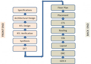
As it shows the design flow starts with a specification document which lists out the technical requirements needed in the chip design. It is followed by translating the specification to Architectural design. The architectural design involves designing the functional blocks and the communication protocol between them and translating them into actual modules that contain FSMs, combinational and sequential circuits etc. The architectural design is then modelled using a Hardware description language like Verilog/VHDL/System Verilog, which is the RTL design stage. The Functional Verification stage starts with a verification plan and a corresponding verification environment which describes and implements the method of proving the design correctness, using different Verification techniques. The design is refined until the HDL model is proved to be meeting the specifications.This stage is followed by Synthesis – a process of transforming the HDL design into a technology specific gate-level netlist, given all the specified constraints and optimization settings. DFT is a structural technique which facilitates a design to become testable after production. All the works till this stage are normally called as the Frontend of VLSI design and are executed by Frontend Engineers.
The next step in the ASIC Design flow is Placement and Routing which involves arranging approximate locations of a set of modules that need to be placed on a layout. Clock tree synthesis is a process which makes sure that the clock gets distributed evenly to all sequential elements in a design to fix the timing violations. This is followed by routing in which exact paths for the interconnection of standard cells and macros and I/O pins are determined.The file produced at the output of the layout is the GDSII (GDS2) file which is the file used by the foundry to fabricate the silicon. Gate level simulations and Static Timing Analysis (a method of validating the timing performance of a design by checking all possible paths for timing violations without having to simulate) are also done to make sure that the gate level design meets the timing requirements for correct design operations. All steps after logic synthesis are performed by Backend engineers and forms the Backend jobs.
Work of a Frontend Engineer
RTL Design/Coding
Synthesis
Functional Verification
DFT
Work of a Backend Engineer
Floor Planning
Placement
Clock Tree Synthesis
STA
Physical Verification
Which one has more career Opportunities?
With the advances being made in technologies like process geometries, feature size and product innovations on a daily basis, there is a constant need to design, develop and re-engineer integrated circuits (ICs). Since electronic products like mobile phones are being released with new features in shorter cycles, there is a healthy demand for qualified VLSI engineers to work on these products. Therefore, there is good scope for a career in the VLSI industry. The important point is that both the domains, front end and back end have their own advantages and have great career prospects. It is completely up to you which one to choose depending on your interest and confidence level, as both offer a great deal of learning and growth.
How to choose?
In order to become a front end engineer, one needs to have good knowledge of HDLs(Verilog/VHDL/SystemVerilog). It will be an added advantage if you have industry related protocol knowledge. So if you have ample digital fundamental knowledge, are fond of HDL coding, love debugging and want to have a sound understanding about the functionality of IC or chip you should definitely go for Front End. With the recent emergence of Artificial intelligence and its application towards VLSI opens up a huge scope for Front end engineers. In order to become a back end engineer, one needs to be well equipped with the concepts of digital electronics, CMOS and Analog Circuits, Scripting knowledge for automation, Hands on Tools for physical design, layout etc. If the above mentioned skills fascinates you then you can opt for Backend and there might be a chance to work in Foundry as well.
Challenges faced by a fresher to get into VLSI industry
Even though VLSI industry is a niche and has lots of career opportunities, on the flip side, industry is currently somewhat less reachable for fresh graduates, compared to other areas due to some particular reasons. Firstly, VLSI or chip design requires a deeper level of knowledge and skills than other electronics related fields .But our Universities are not catering 100% to the VLSI industry requirements. Secondly, VLSI chip design is expensive and requires access to high-cost, specialised electronic design automation (EDA) tools.
How can Chipedge help?
Chipedge offers various courses for fresh graduates both in frontend and backend domains, to choose from. The courses are well structured starting from building a strong foundation by emphasising on fundamental subjects like Digital, CMOS etc. Once the candidate becomes confident with the fundamental knowledge, we impart all the domain specific skills required for the VLSI industry, by giving hands on training on industry standard EDA tools (Synopsys).
1 note
·
View note
Text
FPGA System Design Training - VLSI Guru
In the evolving world of digital design, FPGA System Design Training has become a cornerstone for engineers aspiring to excel in hardware design and embedded systems. VLSI Guru’s comprehensive FPGA System Design course equips you with the skills to design, develop, and implement FPGA-based systems using the latest industry tools and methodologies.
What is FPGA System Design?
FPGA (Field-Programmable Gate Array) System Design involves programming configurable logic blocks to create customized hardware solutions. FPGAs are widely used in applications like embedded systems, signal processing, and high-performance computing due to their flexibility, scalability, and speed.
Why Choose VLSI Guru for FPGA System Design Training?
1. Industry-Focused Curriculum
VLSI Guru’s training covers all essential aspects of FPGA System Design, including:
Basics of FPGA architecture and design flow.
Programming using VHDL and Verilog.
Advanced concepts like timing analysis, IP integration, and system optimization.
Hands-on experience with industry tools like Xilinx Vivado and Intel Quartus.
2. Hands-On Learning
Our training emphasizes practical exposure, allowing you to work on real-world FPGA projects such as:
Designing digital circuits.
Implementing communication protocols.
Developing hardware acceleration modules.
3. Expert Mentorship
Learn from experienced trainers with extensive industry expertise, ensuring you gain insights into real-world FPGA system design challenges and solutions.
4. Placement Assistance
VLSI Guru provides job-oriented training along with resume building, interview preparation, and placement support to help you secure roles in top hardware and semiconductor companies.
What Will You Learn?
Fundamentals of FPGA architecture and HDL programming.
Design, simulation, and implementation using Verilog/VHDL.
Prototyping on FPGA development boards.
Debugging and optimization techniques for FPGA-based systems.
Who Should Enroll?
This course is ideal for:
Engineering graduates in electronics, electrical, or related fields.
Freshers and professionals seeking a career in FPGA System Design.
Embedded system developers looking to enhance their hardware design skills.
Why FPGA System Design is in Demand
FPGAs are the backbone of modern electronics, powering innovations in telecommunications, automotive, IoT, and artificial intelligence. Skilled FPGA engineers are in high demand to meet the growing need for customized hardware solutions.
Join VLSI Guru Today
Get ahead in the competitive semiconductor industry with VLSI Guru’s FPGA System Design Training. Our hands-on approach, expert guidance, and career support ensure you are ready to tackle the challenges of FPGA-based system design.
Contact us now to learn more and take the first step toward an exciting career in FPGA design
0 notes
Text
Agilex 5 E-Series with Power-Optimized Edge Performance
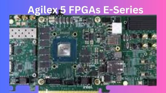
Intel Agilex 5 FGPA
Agilex 5 E-Series
Altera’s latest mid-range FPGAs, the Agilex 5 FPGAs E-Series, are now supported by the recently released Quartus Prime Software v24.1, which can be downloaded right now. Intel are happy to announce that it is now simpler than ever and completely free of charge to take use of the unmatched capability of Altera’s Agilex 5 FPGAs E-Series with the introduction of the state-of-the-art Quartus Prime Software from Altera.
Intel Agilex 5
Free Licence: Get rid of obstacles. With the help of Quartus Prime Pro Edition Software v24.1, you may use the newest E-Series devices at no cost, enabling you to innovate beyond limits!
Streamlined Design Flow: Use Quartus Prime Software to see the smooth integration of intellectual property (IP)-Centric design flow. Their easily customizable design samples streamline the process of getting started so you can concentrate on what really matters your innovative ideas.
New Embedded Processing Capabilities: Make use of the Simics simulator-supported dual-core ARM Cortex-A76 and dual-core ARM Cortex-A55 of the Agilex 5 SoC FPGA, the industry’s first asymmetric processing complex. Additionally, Agilex 5 FPGAs may be combined with the feature-rich, performance- and space-optimized Nios V soft-processor for smaller embedded FPGA applications. Additionally, they collaborate with a number of partners who provide a top-notch suite of tools to improve your FPGA and embedded development experience, including Arm, Wind River, Siemens, Ashling, MathWorks, and many more.
Comprehensive Intellectual Property (IP) Portfolio: With their tried-and-true IP portfolio for Agilex 5 FPGAs, many of which are free, you may shorten the time it takes to market. Reduce the amount of circuitry used and make design timing closure easier with hard IP solutions for PCI Express, Ethernet, and memory protocols, which also support LPDDR5. With PCS’s Ethernet 10G MAC, you can guarantee deterministic and synchronised communication, enhanced by Time-Sensitive Networking (TSN) features.
This version includes the Video and Vision Processing (VVP) portfolio IP for Agilex 5 FPGAs, which enables the entire portfolio of video solutions, as well as additional IPs supporting MIPI D-PHY and MIPI CSI-2. Begin developing your Agilex 5 FPGA designs and rely on additional validated advanced features like JESD204C IP, ORAN IP, LDPC IP, CPRI, and eCPRI among others.
Unprecedented Capabilities: Altera FPGAs may be programmed with cutting-edge capabilities like the following using the Quartus Prime Pro Edition Software v24.1.
Agilex 5 datasheet
Dashboard for Quartus Software Exploration (Preproduction)
With distinct instances of Quartus Prime software, numerous projects running concurrently may be easily coordinated and the compilation and timing results can be seen.
Fresh Features for Compilation: Generation flow of precompiled components (PCCs)Utilising the new precompiled component (PCC) generation flow during compilation, shorten the time it takes to compile synthesis.Start the Simulator using the Quartus Prime GUI.Effortlessly start simulations straight from the Quartus Prime GUI by using the handy “Tools ➤ Run Simulation” menu item. Remove the need for extra procedures to streamline your workflow and save time.
Features and Improvements of Synthesis
Use the RTL Linter Tool to convert older RTL files to Verilog/VHDL standards with ease, optimise RAM inference for better speed and resource use, and reduce warnings in error-free RTL modules to increase readability while developing.
Improved Timing Indicator
Gain more flexibility in timing analysis and SDC scripting with new scripting options; guarantee design integrity with sign-off capabilities for particular combinational loops; and learn more about timing characteristics with enhanced Chip Planner visualisation of asynchronous clock domain crossings (CDCs).
Innovations in Advanced Link Analysers
Link Builder: Use the brand-new Link Builder tool to quickly and easily build high-speed serial connections. Streamline the connection creation procedure by automatically generating schematics and importing channels and devices.
High DPI Monitor Assistance: Benefit from improved readability and display quality thanks to GUI scaling for high DPI displays and automated DPI recognition. Enjoy enhanced usability and user experience.
Enhanced Data Viewer: With improvements to the Data Viewer, analyse forward error correction (FEC) code word faults more effectively. Error outcomes may be easily interpreted and analysed for more efficient error correction techniques.
Enhancements to Simulation Time:
Easy-to-use UI for automated import of devices and channels and schematics. Agilex 7 IP offers faster simulation times with the updated Q run and FEC models.
Qualities:
R-Tile: Transaction Layer (TL) multi-channel DMA IP (AXI) up to Gen5 x16 For flexibility in incorporating third-party PCIe Switch IP, use the bypass mode. A new design example for Gen5 x4 endpoint configuration is also provided.
F-Tile: Utilising FastSIM to reduce simulation time in PIPE mode and providing Ubuntu driver support for all sample designs.increased compatibility for up to 64 embedded endpoints.For greater coverage, the Debug Tool Kit (DTK) was added to the switch IP.
Become a Part of the Community: Hua Xue, VP & GM Software Engineering, remarked, “Intel’re excited to offer Quartus Prime Software v24.1, a crucial milestone in FPGA design.”
“Now, engineers everywhere can easily access the unmatched potential of Agilex 5 FPGAs E-Series.” Quartus’s simplified design process and these cutting-edge technologies allow engineers to reach their full potential for innovation. With their state-of-the-art processing capabilities, Agilex 5 devices transform embedded FPGA applications. These are enhanced by Quartus’s vast IP portfolio, which includes a variety of solutions like Ethernet, PCI Express, memory protocols like LPDDR5, support for MIPI D-PHY, CSI-2, and a suite of video solutions, among many other IPs.
The Quartus Exploration Dashboard offers a user-friendly interface and optimization recommendations, which further improve the design exploration process. Intel’re pushing both the simplicity of use and the fast compiler technologies with Quartus v24.1’s open access to E-Series FPGAs and a simplified design pipeline to enable engineers and innovators to unleash their creativity like never before.”
Intel Agilex 5 price
Normally marketed to corporations and incorporated into bigger systems, the Intel Agilex 5 FPGAs do not have a set pricing that is made accessible to the general public. A number of variables affect the pricing, including:
Model specifics: The Agilex 5 family has two distinct series (D and E) with differing logic cell characteristics and capacities. Models with additional features will cost more.
Volume: If you buy in large quantities, you may be able to negotiate a lower price with distributors or directly with Intel.
Distributor: Price structures may vary significantly throughout distributors.
Read more on Govindhtech.com
#Agilex#intelagilex#agilex5#intelagilex5#govindhtech#FPGA#news#technews#technology#technologynews#TechnologyTrends Intel
0 notes