#FPGA development
Explore tagged Tumblr posts
Visit Tumblr Blog
Explore Tumblr blogs with no restrictions, modern design and the best experience.
Last Seen Tumblr Blogs


Fun Fact
In 2020, Tumblr had 29.4 million users in the US.
Text
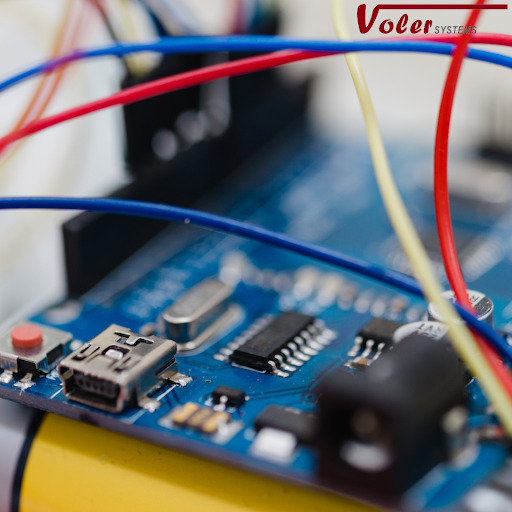
Apart from the FPGA design, Voler Systems formulated the necessary firmware for board functionality testing that enabled to customer to finalize their firmware development. Voler Systems worked closely with their mechanical design team to match the device’s electrical, mechanical, and environmental requirements. Their engineers made sure that the device was functional, durable, and reliable under the extreme conditions, often common during military operations.
#Electronic Design Services#Electronic Product Design#Electronics Design Company#Electronics Design Services#FPGA Design#FPGA Development
1 note
·
View note
Text
Future Electronics to Host Future Tech Day in Hefei, China
Future Electronics, a global leader in electronics distribution, is excited to announce the upcoming "Future Tech Day" portion of the 2024 China Tech Day series—focusing on the automotive industry. The event will take place on Wednesday, September 25th in Hefei, with another session planned in Hangzhou later this year.
#Future Electronics#(SDCs)#Power#MCUs#FPGA#LCDs#Wireless#Lighting#electronic components#Capacitors#Film Capacitors#Analog#development tools#electromechanical
3 notes
·
View notes
Text
Future Electronics' full Advanced Engineering with sharing of engineering ideas
Future Electronics’ Advanced Engineering Group provides in-depth engineering services. Founded in 1968, Future Electronics is a global leader in the electronic components industry. Future Electronics' award-winning customer service, global supply chain programs and industry-leading engineering design services have made the company a strategic partner of choice.
#Future Electronics#(SDCs)#Power#MCUs#FPGA#LCDs#Wireless#Lighting#electronic components#Capacitors#Film Capacitors#Analog#development tools#electromechanical
1 note
·
View note
Text
Future Electronics, recognized their partnership with Infineon
Future Electronics and Infineon Technologies recently hosted a webinar, which taught attendees about the benefits and use cases of Infineon’s cutting-edge memory solutions.
#Future Electronics#(SDCs)#Power#MCUs#FPGA#LCDs#Wireless#Lighting#electronic components#Capacitors#Film Capacitors#Analog#development tools#electromechanical
1 note
·
View note
Text
Future Electronics Invites Employees to Annual Holiday Luncheon
This festive event wraps up Future Electronics’ Spirit of the Holidays initiative. Throughout December, the company will be hosting a series of fun moments to give back to employees and gather food, toys, and monetary donations for those less fortunate.
#Future Electronics#(SDCs)#Power#MCUs#FPGA#LCDs#Wireless#Lighting#electronic components#Capacitors#Film Capacitors#Analog#development tools#electromechanical
1 note
·
View note
Text

A leading aerospace company experienced this challenge head-on while developing a wearable night vision camera designed for military operations. With strict requirements for size, weight, power consumption, and performance, the company required a trustworthy partner with specialized expertise. Voler Systems, well-known for its innovation in FPGA design, electronic design, wearables, and firmware, collaborated to bring this ambitious project to life.
#FPGA Design#FPGA Development#Electronics Product Design#Product Design Electronics#Electronics Design Company#Electronic Design Services
0 notes
Text
Future Electronics, a distributor of electronic components founded in 1968
Future Electronics, a leading global distributor of electronic components, recently received Diodes Incorporated’s Best Global Distributor Award for 2023.
#Future Electronics#Power#MCUs#FPGA#LCDs#Wireless#Lighting#electronic components#Capacitors#Film Capacitors#Analog#development tools#electromechanical
1 note
·
View note
Text
youtube
VHDL Tutorial - Complete Guide to VHDL Process Statement for Beginners [20 mins] [Easy Way]
Welcome to this comprehensive VHDL tutorial where we will dive into the VHDL process statement. In this easy-to-follow guide, we will take you through the syntax and usage of the VHDL process statement, catering especially to beginners. This tutorial will provide you with a thorough understanding of the VHDL process and how it can be effectively implemented in your projects.
Subscribe to "Learn And Grow Community"
YouTube : https://www.youtube.com/@LearnAndGrowCommunity
LinkedIn Group : https://www.linkedin.com/groups/7478922/
Blog : https://LearnAndGrowCommunity.blogspot.com/
Facebook : https://www.facebook.com/JoinLearnAndGrowCommunity/
Twitter Handle : https://twitter.com/LNG_Community
DailyMotion : https://www.dailymotion.com/LearnAndGrowCommunity
Instagram Handle : https://www.instagram.com/LearnAndGrowCommunity/
Follow #LearnAndGrowCommunity
#VHDL tutorial#VHDL process statement#VHDL syntax#VHDL beginner's guide#VHDL tutorial for beginners#VHDL process explained#VHDL process tutorial#VHDL sequential logic#VHDL combinational logic#VHDL development#VHDL design#VHDL FPGA#VHDL ASIC#VHDL circuits#VHDL learning#VHDL education#VHDL digital design#VHDL programming#HDL Design#Digital Design#Verilog#VHDL#FPGA#Simulation#Project#Synthesis#Training#Career#Programming Language#Xilinx
1 note
·
View note
Note
What are some of the coolest computer chips ever, in your opinion?
Hmm. There are a lot of chips, and a lot of different things you could call a Computer Chip. Here's a few that come to mind as "interesting" or "important", or, if I can figure out what that means, "cool".
If your favourite chip is not on here honestly it probably deserves to be and I either forgot or I classified it more under "general IC's" instead of "computer chips" (e.g. 555, LM, 4000, 7000 series chips, those last three each capable of filling a book on their own). The 6502 is not here because I do not know much about the 6502, I was neither an Apple nor a BBC Micro type of kid. I am also not 70 years old so as much as I love the DEC Alphas, I have never so much as breathed on one.
Disclaimer for writing this mostly out of my head and/or ass at one in the morning, do not use any of this as a source in an argument without checking.
Intel 3101
So I mean, obvious shout, the Intel 3101, a 64-bit chip from 1969, and Intel's first ever product. You may look at that, and go, "wow, 64-bit computing in 1969? That's really early" and I will laugh heartily and say no, that's not 64-bit computing, that is 64 bits of SRAM memory.
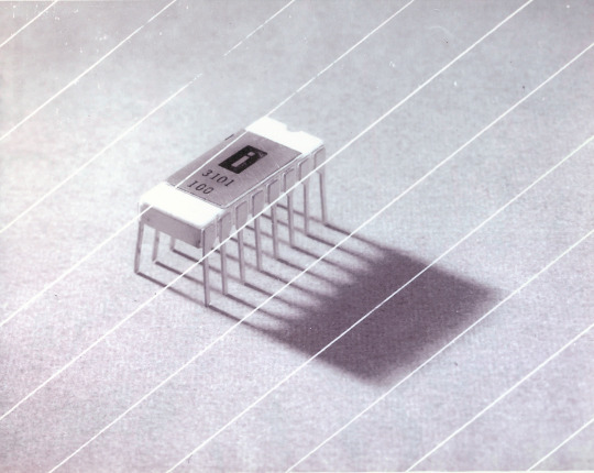

This one is cool because it's cute. Look at that. This thing was completely hand-designed by engineers drawing the shapes of transistor gates on sheets of overhead transparency and exposing pieces of crudely spun silicon to light in a """"cleanroom"""" that would cause most modern fab equipment to swoon like a delicate Victorian lady. Semiconductor manufacturing was maturing at this point but a fab still had more in common with a darkroom for film development than with the mega expensive building sized machines we use today.
As that link above notes, these things were really rough and tumble, and designs were being updated on the scale of weeks as Intel learned, well, how to make chips at an industrial scale. They weren't the first company to do this, in the 60's you could run a chip fab out of a sufficiently well sealed garage, but they were busy building the background that would lead to the next sixty years.
Lisp Chips
This is a family of utterly bullshit prototype processors that failed to be born in the whirlwind days of AI research in the 70's and 80's.
Lisps, a very old but exceedingly clever family of functional programming languages, were the language of choice for AI research at the time. Lisp compilers and interpreters had all sorts of tricks for compiling Lisp down to instructions, and also the hardware was frequently being built by the AI researchers themselves with explicit aims to run Lisp better.
The illogical conclusion of this was attempts to implement Lisp right in silicon, no translation layer.
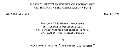
Yeah, that is Sussman himself on this paper.
These never left labs, there have since been dozens of abortive attempts to make Lisp Chips happen because the idea is so extremely attractive to a certain kind of programmer, the most recent big one being a pile of weird designd aimed to run OpenGenera. I bet you there are no less than four members of r/lisp who have bought an Icestick FPGA in the past year with the explicit goal of writing their own Lisp Chip. It will fail, because this is a terrible idea, but damn if it isn't cool.
There were many more chips that bridged this gap, stuff designed by or for Symbolics (like the Ivory series of chips or the 3600) to go into their Lisp machines that exploited the up and coming fields of microcode optimization to improve Lisp performance, but sadly there are no known working true Lisp Chips in the wild.
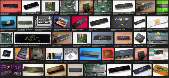
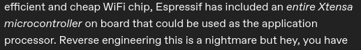
Zilog Z80
Perhaps the most important chip that ever just kinda hung out. The Z80 was almost, almost the basis of The Future. The Z80 is bizzare. It is a software compatible clone of the Intel 8080, which is to say that it has the same instructions implemented in a completely different way.
This is, a strange choice, but it was the right one somehow because through the 80's and 90's practically every single piece of technology made in Japan contained at least one, maybe two Z80's even if there was no readily apparent reason why it should have one (or two). I will defer to Cathode Ray Dude here: What follows is a joke, but only barely

The Z80 is the basis of the MSX, the IBM PC of Japan, which was produced through a system of hardware and software licensing to third party manufacturers by Microsoft of Japan which was exactly as confusing as it sounds. The result is that the Z80, originally intended for embedded applications, ended up forming the basis of an entire alternate branch of the PC family tree.
It is important to note that the Z80 is boring. It is a normal-ass chip but it just so happens that it ended up being the focal point of like a dozen different industries all looking for a cheap, easy to program chip they could shove into Appliances.
Effectively everything that happened to the Intel 8080 happened to the Z80 and then some. Black market clones, reverse engineered Soviet compatibles, licensed second party manufacturers, hundreds of semi-compatible bastard half-sisters made by anyone with a fab, used in everything from toys to industrial machinery, still persisting to this day as an embedded processor that is probably powering something near you quietly and without much fuss. If you have one of those old TI-86 calculators, that's a Z80. Oh also a horrible hybrid Z80/8080 from Sharp powered the original Game Boy.
I was going to try and find a picture of a Z80 by just searching for it and look at this mess! There's so many of these things.
I mean the C/PM computers. The ZX Spectrum, I almost forgot that one! I can keep making this list go! So many bits of the Tech Explosion of the 80's and 90's are powered by the Z80. I was not joking when I said that you sometimes found more than one Z80 in a single computer because you might use one Z80 to run the computer and another Z80 to run a specialty peripheral like a video toaster or music synthesizer. Everyone imaginable has had their hand on the Z80 ball at some point in time or another. Z80 based devices probably launched several dozen hardware companies that persist to this day and I have no idea which ones because there were so goddamn many.
The Z80 eventually got super efficient due to process shrinks so it turns up in weird laptops and handhelds! Zilog and the Z80 persist to this day like some kind of crocodile beast, you can go to RS components and buy a brand new piece of Z80 silicon clocked at 20MHz. There's probably a couple in a car somewhere near you.
Pentium (P6 microarchitecture)
Yeah I am going to bring up the Hackers chip. The Pentium P6 series is currently remembered for being the chip that Acidburn geeks out over in Hackers (1995) instead of making out with her boyfriend, but it is actually noteworthy IMO for being one of the first mainstream chips to start pulling serious tricks on the system running it.

The P6 microarchitecture comes out swinging with like four or five tricks to get around the numerous problems with x86 and deploys them all at once. It has superscalar pipelining, it has a RISC microcode, it has branch prediction, it has a bunch of zany mathematical optimizations, none of these are new per se but this is the first time you're really seeing them all at once on a chip that was going into PC's.
Without these improvements it's possible Intel would have been beaten out by one of its competitors, maybe Power or SPARC or whatever you call the thing that runs on the Motorola 68k. Hell even MIPS could have beaten the ageing cancerous mistake that was x86. But by discovering the power of lying to the computer, Intel managed to speed up x86 by implementing it in a sensible instruction set in the background, allowing them to do all the same clever pipelining and optimization that was happening with RISC without having to give up their stranglehold on the desktop market. Without the P5 we live in a very, very different world from a computer hardware perspective.
From this falls many of the bizzare microcode execution bugs that plague modern computers, because when you're doing your optimization on the fly in chip with a second, smaller unix hidden inside your processor eventually you're not going to be cryptographically secure.
RISC is very clearly better for, most things. You can find papers stating this as far back as the 70's, when they start doing pipelining for the first time and are like "you know pipelining is a lot easier if you have a few small instructions instead of ten thousand massive ones.
x86 only persists to this day because Intel cemented their lead and they happened to use x86. True RISC cuts out the middleman of hyperoptimizing microcode on the chip, but if you can't do that because you've girlbossed too close to the sun as Intel had in the late 80's you have to do something.
The Future
This gets us to like the year 2000. I have more chips I find interesting or cool, although from here it's mostly microcontrollers in part because from here it gets pretty monotonous because Intel basically wins for a while. I might pick that up later. Also if this post gets any longer it'll be annoying to scroll past. Here is a sample from a post I have in my drafts since May:
I have some notes on the weirdo PowerPC stuff that shows up here it's mostly interesting because of where it goes, not what it is. A lot of it ends up in games consoles. Some of it goes into mainframes. There is some of it in space. Really got around, PowerPC did.
237 notes
·
View notes
Text
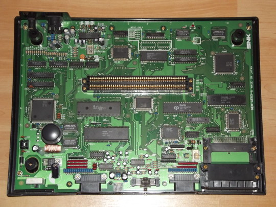
Hell is terms like ASIC, FPGA, and PPU
I haven't been doing any public updates on this for a bit, but I am still working on this bizarre rabbit hole quest of designing my own (probably) 16-bit game console. The controller is maybe done now, on a design level. Like I have parts for everything sourced and a layout for the internal PCB. I don't have a fully tested working prototype yet because I am in the middle of a huge financial crisis and don't have the cash laying around to send out to have boards printed and start rapidly iterating design on the 3D printed bits (housing the scroll wheel is going to be a little tricky). I should really spend my creative energy focusing on software development for a nice little demo ROM (or like, short term projects to earn money I desperately need) but my brain's kinda stuck in circuitry gear so I'm thinking more about what's going into the actual console itself. This may get techie.
So... in the broadest sense, and I think I've mentioned this before, I want to make this a 16-bit system (which is a term with a pretty murky definition), maybe 32-bit? And since I'm going to all this trouble I want to give my project here a little something extra the consoles from that era didn't have. And at the same time, I'd like to be able to act as a bridge for the sort of weirdos who are currently actively making new games for those systems to start working on this, on a level of "if you would do this on this console with this code, here's how you would do it on mine." This makes for a hell of a lot of research on my end, but trust me, it gets worse!
So let's talk about the main strengths of the 2D game consoles everyone knows and loves. Oh and just now while looking for some visual aids maybe I stumbled across this site, which is actually great as a sort of mid-level overview of all this stuff. Short version though-
The SNES (or Super Famicom) does what it does by way of a combination of really going all in on direct memory access, and particularly having a dedicated setup for doing so between scanlines, coupled with a bunch of dedicated graphical modes specialized for different use cases, and you know, that you can switch between partway through drawing a screen. And of course the feature everyone knows and loves where you can have one polygon and do all sorts of fun things with it.
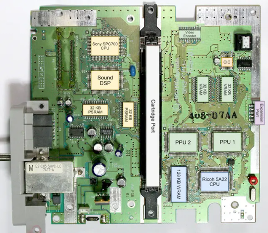
The Genesis (or Megadrive) has an actual proper 16-bit processor instead of this weird upgraded 6502 like the SNES had for a scrapped backwards compatibility plan. It also had this frankly wacky design where they just kinda took the guts out of a Sega Master System and had them off to the side as a segregated system whose only real job is managing the sound chip, one of those good good Yamaha synths with that real distinct sound... oh and they also actually did have a backwards compatibility deal that just kinda used the audio side to emulate an SMS, basically.
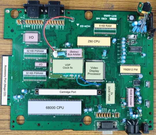
The TurboGrafix-16 (or PC Engine) really just kinda went all-in on making its own custom CPU from scratch which...we'll get to that, and otherwise uh... it had some interesting stuff going on sound wise? I feel like the main thing it had going was getting in on CDs early but I'm not messing with optical drives and they're no longer a really great storage option anyway.
Then there's the Neo Geo... where what's going on under the good is just kind of A LOT. I don't have the same handy analysis ready to go on this one, but my understanding is it didn't really go in for a lot of nice streamlining tricks and just kinda powered through. Like it has no separation of background layers and sprites. It's just all sprites. Shove those raw numbers.
So what's the best of all worlds option here? I'd like to go with one of them nice speedy Motorolla processors. The 68000 the Genesis used is no longer manufactured though. The closest still-in-production equivalent would be the 68SEC000 family. Seems like they go for about $15 a pop, have a full 32-bit bus, low voltage, some support clock speeds like... three times what the Genesis did. It's overkill, but should remove any concerns I have about having a way higher resolution than the systems I'm jumping off from. I can also easily throw in some beefy RAM chips where I need.
I was also planning to just directly replicate the Genesis sound setup, weird as it is, but hit the slight hiccup that the Z80 was JUST discontinued, like a month or two ago. Pretty sure someone already has a clone of it, might use that.
Here's where everything comes to a screeching halt though. While the makers of all these systems were making contracts for custom processors to add a couple extra features in that I should be able to work around by just using newer descendant chips that have that built in, there really just is no off the shelf PPU that I'm aware of. EVERYONE back in the day had some custom ASIC (application-specific integrated circuit) chip made to assemble every frame of video before throwing it at the TV. Especially the SNES, with all its modes changing the logic there and the HDMA getting all up in those mode 7 effects. Which are again, something I definitely want to replicate here.
So one option here is... I design and order my own ASIC chips. I can probably just fit the entire system in one even? This however comes with two big problems. It's pricy. Real pricy. Don't think it's really practical if I'm not ordering in bulk and this is a project I assume has a really niche audience. Also, I mean, if I'm custom ordering a chip, I can't really rationalize having stuff I could cram in there for free sitting outside as separate costly chips, and hell, if it's all gonna be in one package I'm no longer making this an educational electronics kit/console, so I may as well just emulate the whole thing on like a raspberry pi for a tenth of the cost or something.
The other option is... I commit to even more work, and find a way to reverse engineer all the functionality I want out with some big array of custom ROMs and placeholder RAM and just kinda have my own multi-chip homebrew co-processors? Still PROBABLY cheaper than the ASIC solution and I guess not really making more research work for myself. It's just going to make for a bigger/more crowded motherboard or something.
Oh and I'm now looking at a 5V processor and making controllers compatible with a 10V system so I need to double check that all the components in those don't really care that much and maybe adjust things.
And then there's also FPGAs (field programmable gate arrays). Even more expensive than an ASIC, but the advantage is it's sort of a chip emulator and you can reflash it with something else. So if you're specifically in the MiSTer scene, I just host a file somewhere and you make the one you already have pretend to be this system. So... good news for those people but I still need to actually build something here.
So... yeah that's where all this stands right now. I admit I'm in way way over my head, but I should get somewhere eventually?
11 notes
·
View notes
Text
- Cheap Chinese XC7K480T FPGA
- BSP & Reverse Engineering Docs from Chinese Github Repo
- Pirate software license from Chinese CSDN site so that I can actually use the larger FPGA chip
I am in full support of continuing relations with 🇨🇳 as they were so that I can have my little enthusiast/hobbyist FPGA environment & develop accelerators for novel encryption primitives.
3 notes
·
View notes
Text
fading's studyblr
Hey y'all
I'm fading, a computer engineering undergrad
Interested Sectors: SWE, Hardware Development
Languages: C/C++, ARM, VHDL, Java, Python
Hardware Technologies: FPGA, nRF 52840 series
SWE Tools: Git, Linux, PowerShell, Quartus Prime, Keil uVision
I'm interested tracking real progress, especially when it comes to developing progress with projects or learning languages
Follow me for tech talks, progress, and more!
follow me on my main: @fadingintogrey
2 notes
·
View notes
Text
AMD Versal AI Engine: Powering Next-Gen Intelligence

What is Versal AI engine?
The Versal Premium line, which integrates AI Engines, has exceptional adaptive signal processing capability and is designed for the most demanding compute and data transportation applications in wired communications, data center computation, test and measurement, and aerospace and military.
Versal AI Engine
The AI Engine Array Interface may be configured with to the AMD LogiCORE AI Engine IP. Through tiles included in the AI Engine Array Interface, this array is linked to both the Network on Chip and the programmable logic (PL). This IP specifies the clock controlling the AI Engine array and permits the definition of the number of AXI4-Stream and memory-mapped AXI interfaces with their corresponding width and orientation.
Key Features and Benefits
AXI4 configuration interfaces that are memory mapped.
AXI4 master interfaces that are memory mapped.
AXI4-Stream master and slave interfaces having 32, 64, or 128 bit data widths that may be adjusted.
Fast streams may be enabled by choosing to enable registered interfaces.
Programmable logic (PL) stream clocks automatically associate.
Designing AMD Versal AI Engine
Image Credit To AMD
AMD Developing Versal AI Engine with Vitis Model Composer AMD With Vitis Model Composer, algorithms designed for Versal AI Engines may be quickly simulated, explored, and coded from inside the Simulink environment. This may be accomplished by importing kernels and data-flow graphs into Vitis Model Composer as blocks and adjusting the block GUI parameter to control the behavior of the kernels and graphs, or by utilizing the AI Engine library blocks.
Additionally, the tool lets you use a combination of AI Engine and programmable logic (HDL/HLS) blocks to create and simulate a design. By seamlessly integrating Vitis Model Composer AI Engine blocks with Simulink source and sink blocks, simulation results may be viewed.
For usage in the Simulink environment, Vitis Model Composer offers a collection of blocks that are optimized for speed. These consist of:
AI Engine blocks
Image Credit To AMD
Comprises a collection of intricate AI Engine DSP building elements pertaining to mixers, FIR, FFT, and DDS.
includes blocks for importing graphs and kernels that may be directed to Versal devices’ AI Engine section.
HLS (Targeting PL and generates HLS code)
Targeting PL and producing HLS code, HLS provides preset blocks that contain bit-wise operations, logic, linear algebra, and math functional blocks.
Block the import of HLS kernels that are intended for Versal devices’ PL section.
HDL (Produces RTL code and targets PL)
Blocks for modeling and synthesizing DSP, arithmetic, and logic components on an FPGA
contains a FIR Compiler block that targets the Versal design’s specific DSP48E1 and DSP48E2 hardware resources.
Blocks that facilitate communication between the AMD HDL blockset and the AI Engine.
Unleash DSP Compute with AMD Versal AI Engines
For next-generation DSP workloads, speed up demanding high-performance DSP applications.
AMD Versal AI Engine Technology Enables High-Performance Digital Signal Processing (DSP) Requirements
Clients developing next-generation DSP applications need enormous computational power, which conventional FPGA designs cannot effectively provide. Large quantities of DSP blocks and programmable logic resources may be used by compute-intensive DSP applications like FIR, FFT, and General Matrix Multiply.
The total computation capability that conventional programmable logic devices may provide may be greatly diminished by this need. For demanding DSP workloads with stringent power constraints, just expanding the number of DSP blocks and programmable logic available is not a scalable solution.
In these situations, Versal AI Engines are intended to provide a more effective computing solution.
Boost Compute and Use Less Power
Optimize performance and transform your DSP designs.
Did you know that you may increase scalability and efficiency to satisfy the growing needs of high-performance, next-generation DSP applications? Learn 5 strategies to improve your DSP designs using AMD Versal AI Engines.
Access Benchmarks Comparing Versal AI Engines to Previous Programmable Logic Technology
Please get in touch with sales or your FAE for test results and source designs for head-to-head benchmark comparisons between designs that use just Programmable Logic and adaptable SoC + AI Engine designs that use AMD Versal adaptable SoCs.
Get Started with Versal AI Engines for DSP
Increase DSP compute density for the next generation of demanding DSP workloads by speeding up the most demanding high-performance DSP applications.
Read more on govindhtech.com
#AMDVersalAIEngine#PoweringNextGenIntelligence#AIEngine#FPGA#AMDVersal#KeyFeatures#AMD#DesigningAMD#AIEngineblocks#DSPCompute#technology#technews#news#govindhtech
2 notes
·
View notes
Text
Handheld LCD Shader Projects
Welcome to the introduction of a collection of the handheld LCD shaders that emulates the colorspace and LCD metrics from the offical handheld gaming consoles. Ranging from Gameboy Color to the PSP being the main focus for emulating the displays from their colorspace to specified gamma and color temperatures. Most users would be playing Gameboy Color and Gameboy Advance in raw RGB on emulators as well as on the Gameboy Player, and that's totally cool. Playing these games on the backlit displays have been much easier to see the game you're playing than ones without any light on the LCDs. Heck, even having much better contrast that gives off darker blacks, or even perfect blacks from OLEDs. However, once you start playing some of those games, you can really see something off from those games from your childhood handheld consoles, most prominent, the Gameboy Color and the Gameboy Advance. Those screens are really different from modern displays we use on a daily basis, on every single specifications. GBC and GBA would look too saturated and odd color hues in a lot of games, under raw RGB picture. In GBA's case, a lot of games can have lighter gamma that looks overbrightened in raw RGB, since those were only calibrated for the old GBA screens that has darker gamma. Oversaturation from those games were also calibrated for these older displays that has less saturation. This project is meant to replicate the colors and gamma from the real console model, to any project, such as emulators, Gameboy Interface, scalers like the Retrotink 4K, LCD mods, and HDMI/FPGAs projects. It would allow users to pick any shaders or LUT textures to replicate the LCD color display to your preferred way to play games beyond pure original hardware. Of course, there is also Nintendo DS from the first model, the DS Lite, Gameboy SP AGS-101 (Backlit version), Gameboy Micro, and the PSP on its first model, as of current. The project is also meant to preserve the display data and metrics from those handhelds.
(GBC shader preset with default settings)
(GBA shader preset with default gamma, and LUT set to "2" for colder greyscale)
(NDS shader preset with default settings)
(PSP shader preset with LUT set to "2" for PSP's known colder greyscale)
Downloads:
Instructions: If you haven't already installed shaders, do so inside retroarch under slang shaders. After downloading my package, extract the zip file to "shaders_slang" inside Retroarch's shader folder. It can be implemented inside libretro's shader once the slang shader pack gets updated. I suggest loading the shaders by presets, under .slangp, in both Handheld and Reshade folder (latter being under the handheld-color-LUTs folder). Presets inside handheld folder has switchable settings, including presets containing LCD shaders. Presets inside reshade only loads in LUT textures rather than just shaders. Useful for emulators or projects that only loads in LUT textures as their only filter.
The shaders is based on HunterK's shader, Color-Mangler from the misc folder in slang shaders from Libretro, which was made from a help for my project. It defaults to sRGB on the shader's option for many average users. A shader preset from Handheld folder has LUT choices to change the greyscale color temperature replicated from the real handheld console. GBA one can adjust the gamma to make the image darker, while GBC and GBM has gamma option to brighten or darken. In Reshade, it only had adjustable greyscale temperature except for GBA_GBC variant. The shader supports DCI-P3 and Rec2020 colorspaces on its option to use on your display that may support either of those to reach better color saturation to present more accurate blue primary color from my shaders that common sRGB colorspace is limited from. The GBA and GBC have external gamma options to adjust the gamma on the greyscales if not using any LUT shader preloaded.
Developer notice: For developers of any GB/GBA (or any handheld) projects involving emulators, FPGAs, or screen mods, shall take some advices when it comes to implementing the shader or color filter to your projects. To implement as a shader, the gamma has to be lower first by 1/2.2 (Can be used to change the GBA gamma itself to darken the screen), then use my color values from the shader to change the color primaries, and then revert the gamma by 2.2 afterwards to have great color correction while respecting luminance and color tones. Also I prefer if you take color values from white balance correction that are outside of GBC/GBA shader. For only LUT texture, a more easy approach for devs, I prefer using the non-cold variants if preserving the greyscale color tone. GBA and GBC LUTs have their gamma and greyscale adjusted to emulate the screen's default gamma. If you only want just the color gamut correction as an LUT, use the GBA_GBC variant inside Reshade's LUT folder. -If you decide to implement a basic GBC or GBA colorspace to the emulator, use the sRGB data. The gamma change must happen before the color correction. -If the project is aimed for TV such as Gameboy Interface or GBA Consolizer, use the sRGB LUT shader, since SD and HDTV resolutions aim for sRGB colorspace. -If the FPGA such as Analogue Pocket, IPS screen mods, or emulation device uses a display gearing towards sRGB colorspace, use the shader, color filter, or LUT accordingly. -If the OLED screen mods or emulation devices have its native colorspace target around 100% DCI-P3 Volume, use any filter accordingly. -If implementing the shader to your emulation project, do port the shader to your shader or filter libraries. The shader and LUTs are in public domain after all, to spread about the color correction regarding GBC/GBA displays. -If using a professional scaler like Retrotink 4K with either GBA Consolizer or Gameboy Interface without any filters used, play with its gamut matrix settings for both GBC and GBA as "Red: 0.4925 0.3100" "Green: 0.3150 0.4825" "Blue 0.1625 0.1925" to emulate the color correction, and can be used on SDR or HDR mode to give out consistent image. Gamut info for other consoles below.
(Raw RGB, Gameboy Micro, and GBA shader with darken set to 0)
(Top: NDS; Raw RGB, DS-Lite, and NDS Phat)
(Bottom: GBA; Raw RGB, GBA-SP AGS-101, and GBA with darken set to 0)
Note: While DS-Lite and SP-101 are really close to sRGB that developers don't really need adjustments, it is shown to preserve on how far they reached from older models to newer ones in mid to late 2000s.
Story:
So when did I start the project and why I was invested in doing this? It was back in August 2014 when I first saw a forum on someone wanting to desaturate the GBA and mentioned the filters from emulators like VisualBoyAdvance, or VBA-M, as well as NO$GBA that has options to emulate the colorspace that is close to the real hardware. I was reminded how the latter emulator has those options when I used it long time ago. I mostly use unfiltered colors as that was how close it looks on my GBA-SP with "Better Screen" than the GBA. Yeah I actually have the backlit version of GBA-SP known as AGS-101. The display was a huge jump from old GBA to GBA-SP, as well as the Nintendo DS Phat under GBA. However, I had good amount of memories of playing my old GBA with the lights around me and I do remember the color saturation being very different overall. So I wanted to take a look on how to replicate the VBA-M's colorspace.
(Link to the forum I created of my histories of re-creating the GBA colors)
I first decide to use simple desaturation with a mix of shaders by playing with saturation and contrast levels. At first, it looks very similar to how VBA-M's attempt looked. That is, until I saw the blue color has a different hue, being more torqourise in VBA-M's recreation. Then a LUT shader appeared in libretro forums and I first used that for my photoshop to use crazy amount of filters to recreate the whole thing, even though it wasn't perfect, but close. Then I tried to replicate the original NDS model that I have for many years, and also played with the LUT textures from Photoshop. Yeah I just simply tried to copy the colors from the console, without any tools, on my uncalibrated old LCD TN panel screen, because I had such no experience on how colorspaces work, but it was worth a try. Then in 2015, I somehow found a shader that plays with RGB and I got help with Hunterk, a contributor on Libretro who has been involved with a lot of shaders for Retroarch. He made an amazing color mangler shader for me to put data of colors and gamma on the shader itself than just using a LUT texture. Then in May of 2015, I found another GBA on my house that was not used by a family for a long time. Yeah I lost my GBA somehow as a kid from another family, but a long story to tell. Thankfully I was allowed to use another GBA for full use just for this project. This was just the beginning of my progress on grabbing screen data starting with just a flashlight with my old LCD monitor. The only issue I always have is the common sRGB screens don't have deep blue colors that is needed for both GBA and NDS (and more), so I always had issues replicating the blue primary color. That's what got me to start learning about colorspace and what sRGB and color gamut means. And that's where my progress to get the right tools begins. I then later got a superior IPS 1080p monitor, the GBC, Colormunki Display, using DisplayCal and HCFR, Colormunki Photo, the PSP, GBA Micro, a 4K monitor, and a portable light to use on GBC and GBA. Now in 2024, I have really progressed with help of such tools I need, have become much better way of getting the LCD data from the handhelds to contain the color gamut, the greyscale, gamma, and color temperature.
So now the story is out of the way, here are the tools I used to gather infos from the handheld screens.
Samsung S80AU - A 4K IPS Monitor that supports DCI-P3 colorspace with great Delta Error scores especially for sRGB colorspace. It's also used to test out LCD shaders on a high DPI display. Colormunki Display - A Colorimeter that calibrates your display and gathers color data from your target screen. Colormunki Photo - A Spechrometer that behaves the same as Display, except gathers the white colors temperatures more accurately regardless on any type of LCD or OLED displays. It's used to make profiles for the Display to be calibrated for a specific monitors as the Display reads data much faster than Photo as well as reading darker blacks better. Displaycal has infos on colormeter matrix correction to add in why this combo is best used for serious color calibration. It's also used primarily for handheld console displays to sample color data. DisplayCal - Used to completely calibrate my monitor and other screens to give off pure sRGB colorspace with 6500K whitepoint. It's also used with its own ICC Profile creator to make .icc with given data from ColorHCFR for a specific Handheld Console display to emulate from. It's 3DLUT tool was also used to generate LUT textures to check the color and luminance on primary and secondary colors. ColorHCFR - A free alternative for Calman. It's used to gather data on the greyscale, the color gamut, and tons more info to check how your targeted display looks. It shows you graphical images of the screen's color gamut on the CIE diagram. MCH2 - A tool that used your generated DisplayCal monitor calibration data to create an .icc profile made for Windows 11 to convert the entire screen to your targeted colorspace such as sRGB and DCI-P3. G2 Pocket RGB Camera Light - A portable light that shoots out lights to use on handhelds that lacks any light, such as the Gameboy Color and Gameboy Advance. It toggles between RGB and pure whitelights with color temperature adjustments. It's used to match the whitepoint on both GBC and GBA to match my monitor's whitepoint as the closest. It's much better tool than me previously using my collection of phones to use the flashlight for color sampling, as GBC and GBA suffers from rainbowing, no adjustments on white balance, and less saturation by a flashlight, unlike proper lights like the G2 Pocket that eliminates those issues. 240p Test Mini - The handheld version of the well known 240p Test Suite. Used to check RGB, greyscale, motion flickering, and color scrolling on real hardware. https://github.com/pinobatch/240p-test-mini EZ Flash Jr - A GB/GBC Flashcarts to load ROMs and Homebrew for GBC and GBA. EZ Flash 3-in-1 Expansion Pack NDS - A GBA Cartridge to load in a ROM and homebrew in to load inside GBA and NDS. Used NDS to insert a ROM on its NOR memory. GIMP - A Photoshop-like image editor that is used to check generated LUTs from 3DLUT to check on the color values to adjust the shader. Retroarch - Using mGBA and Sameboy emulator core to check out the games while using the shaders I created for color correction. It also loads in image files for my best way to check out my shaders during adjustments.
(Top to Bottom: gba-color & gbc-color, gbMicro-color, nds-color, psp-color, DSLite-color, SP101-color, and raw RGB, all in sRGB)
Note: Why the white color is darker is due to clipping on the yellow color because of how color correction works with the blue color being out of sRGB gamut. Also, sRGB can't display those handhelds blue saturation due to it. Will soon post DCI-P3 and Rec2020 variants for displays that can see more saturation without internal color adjustments.
List of handheld consoles I owned to create shaders out of: Gameboy Color Gameboy Advance Gameboy Advance SP (AGS-101) Gameboy Micro Nintendo DS Nintendo DS Lite PSP (1000)
Nintendo Switch Online emulates GBC and GBA with their own color filters. GBA only desaturates the screen in more simple manner for sRGB, which was easy to implement. GBC, was very hard to do in shaders currently, so to use full experience, the LUT version can only be used to fully emulate the effect for other emulators.
I also found someone's Switch OLED data from a youtube video. The colorspace is taken with bigger saturation than even DCI-P3 when using vivid mode. Here's a link to the video by GamingTech:
youtube
I also made Palm Treo 700p shader long time ago by taking DisplayMate's data long ago while trying to translate the gamut pin points to HCFR since I don't have those in possession. I only made it for experiment long ago and only archived.
Replicating existing filters from emulators or dev tools such as No&GBA and VBA-M for GBA image replication, and GBC tools like Gameboy HiColour Converter V1.2 for GBC image replications. Even No$GBA and No$GMB docs had mentioned the LCD color differences:
(HiColour Convertor)
My Handheld LCD review datasheet and showcase for each platform (Coming Soon):
Gameboy Color Gameboy Advance Gameboy Advance SP AGS-101 Gameboy Micro Nintendo DS (Phat) Nintendo DS Lite PSP-1000
Handheld consoles I plan on getting and make data out of: PSP-3000 or GO PS Vita Nintendo 3DS (Owned, but not yet examined)
Handhelds I don't plan on getting or reviewing: Gameboy or Gameboy Pocket (Many have made their own shaders and filters out of their monochromic display) Gameboy Advance SP AGS-001 (Uses the same exact display as the original GBA except with frontlight added) Knockoff GB Boy Colour (I only allow any official handheld consoles for my project) PSP-2000 (Same colorspace and data as PSP-1000, except brighter screen) PS-Vita 2000 (Uses LCD instead of OLED, with less color gamut than original PS Vita) Nintendo NEW 2DS XL/3DS (or XL) IPS displays (Hard to find and a lottery to obtain; not common) Nintendo Switch (Owned and targets sRGB and its gamma well; whitepoint can vary between units)
Notes: On GBA, A lot of games are calibrated for the GBA's gamma due to how dark its screen's gamma looks. For some games, often Nintendo and a couple of companies with closest relationship to Nintendo, are adjusted for its colorspace. Certain games, often SNES ports, may have its original palettes on its setting. On GBC, many games were made for the screen during its run. It's unknown which amount of games weren't calibrated for the screen. Although certain games like Link's Adventure DX were completely adjusted for the screen on colorspace, gamma, and color temperature, which made purple-grey colors looks more grey overall. On both NDS and PSP, pretty often the first few years of games can be adjusted for those screens. Those are until both NDS-Lite and PSP-3000 have colorspace that closely aims for sRGB where no adjustments can be made. Many multi-ports for PSP of the same game from home consoles are very likely not calibrated for the first two PSP models. I didn't make a Switch OLED preset (from Vivid mode) with LCD shader, since the Switch OLED is not LCD, its RGB pattern is very different, and either original LCD or OLED are too high resolution to notice its RGB patterns. It's best to use only the shader to use with Reshade on a Switch emulator to emulate the OLED's vivid mode, but preserved in Libretro to see its effect. While I explain what the shaders are meant to use for, it's also your preference on using the shaders or just using the Raw RGB colors that fits your needs. You can use other color shaders on a GBA or GBC emulator, such as using NDS, Micro, or PSP shaders to your preference. The PSP shaders have much more saturation than any Gameboy line or NDS Phat, while preserving its hue.
To end off on this page, I would also like to give respect to other projects that tried their attempt to create their own color correction. While I prefer the best accuracy of the color correction from my shaders, many of their color corrections are pretty impressive with varying degree levels of accuracy, and they all motivate me to continue with the project to give out the best quality of color correction. Their blogs have pretty interesting ideas on how displays work on GBC and GBA.
(BGB's "Reality" Color Correction filter)
(GBCC's page on GBC screen tech notes)
(Bsnes/Higan Color emulation page)
(Gameboy Interface having their own Color Matrix correction, and including our shaders and filters alongside)
youtube
(Nintendo showing their GBC and GBA color correction under Virtual Console from Nintendo Switch Online, the former having bigger difference)
#gameboy advance#gameboy color#nintendo ds#playstation portable#gbc#gba#nds#psp#colors#handheld#shaders#libretro#retroarch#emulation#emulators#gameboy micro#color correction#colorspace#nintendo switch oled
5 notes
·
View notes
Text
FPGA Market - Exploring the Growth Dynamics

The FPGA market is witnessing rapid growth finding a foothold within the ranks of many up-to-date technologies. It is called versatile components, programmed and reprogrammed to perform special tasks, staying at the fore to drive innovation across industries such as telecommunications, automotive, aerospace, and consumer electronics. Traditional fixed-function chips cannot be changed to an application, whereas in the case of FPGAs, this can be done. This brings fast prototyping and iteration capability—extremely important in high-flux technology fields such as telecommunications and data centers. As such, FPGAs are designed for the execution of complex algorithms and high-speed data processing, thus making them well-positioned to handle the demands that come from next-generation networks and cloud computing infrastructures.
In the aerospace and defense industries, FPGAs have critically contributed to enhancing performance in systems and enhancing their reliability. It is their flexibility that enables the realization of complex signal processing, encryption, and communication systems necessary for defense-related applications. FPGAs provide the required speed and flexibility to meet the most stringent specifications of projects in aerospace and defense, such as satellite communications, radar systems, and electronic warfare. The ever-improving FPGA technology in terms of higher processing power and lower power consumption is fueling demand in these critical areas.
Consumer electronics is another upcoming application area for FPGAs. From smartphones to smart devices, and finally the IoT, the demand for low-power and high-performance computing is on the rise. In this regard, FPGAs give the ability to integrate a wide array of varied functions onto a single chip and help in cutting down the number of components required, thereby saving space and power. This has been quite useful to consumer electronics manufacturers who wish to have state-of-the-art products that boast advanced features and have high efficiency. As IoT devices proliferate, the role of FPGAs in this area will continue to foster innovation.
Growing competition and investments are noticed within the FPGA market, where key players develop more advanced and efficient products. The performance of FPGAs is increased by investing in R&D; the number of features grows, and their cost goes down. This competitive environment is forcing innovation and a wider choice availability for end-users is contributing to the growth of the whole market.
Author Bio -
Akshay Thakur
Senior Market Research Expert at The Insight Partners
2 notes
·
View notes