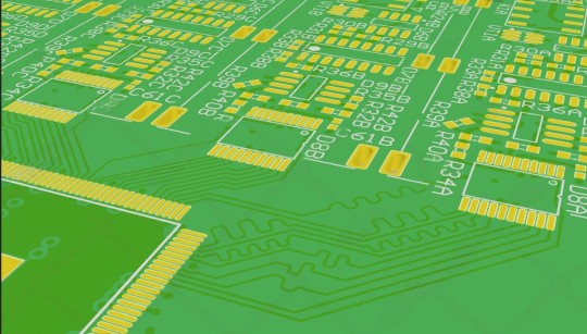
#differences between PCB design and PCB layout
Explore tagged Tumblr posts
Visit Tumblr Blog
Explore Tumblr blogs with no restrictions, modern design and the best experience.
Last Seen Tumblr Blogs


Fun Fact
Post activity is at the highest at 4:00 pm EDT; notes peak at 10:00 pm EDT.
Text
Understand the key differences between PCB design and PCB layout. Learn how each process plays a critical role in creating efficient printed circuit boards.
0 notes
Text
Hell is terms like ASIC, FPGA, and PPU
I haven't been doing any public updates on this for a bit, but I am still working on this bizarre rabbit hole quest of designing my own (probably) 16-bit game console. The controller is maybe done now, on a design level. Like I have parts for everything sourced and a layout for the internal PCB. I don't have a fully tested working prototype yet because I am in the middle of a huge financial crisis and don't have the cash laying around to send out to have boards printed and start rapidly iterating design on the 3D printed bits (housing the scroll wheel is going to be a little tricky). I should really spend my creative energy focusing on software development for a nice little demo ROM (or like, short term projects to earn money I desperately need) but my brain's kinda stuck in circuitry gear so I'm thinking more about what's going into the actual console itself. This may get techie.
So... in the broadest sense, and I think I've mentioned this before, I want to make this a 16-bit system (which is a term with a pretty murky definition), maybe 32-bit? And since I'm going to all this trouble I want to give my project here a little something extra the consoles from that era didn't have. And at the same time, I'd like to be able to act as a bridge for the sort of weirdos who are currently actively making new games for those systems to start working on this, on a level of "if you would do this on this console with this code, here's how you would do it on mine." This makes for a hell of a lot of research on my end, but trust me, it gets worse!
So let's talk about the main strengths of the 2D game consoles everyone knows and loves. Oh and just now while looking for some visual aids maybe I stumbled across this site, which is actually great as a sort of mid-level overview of all this stuff. Short version though-
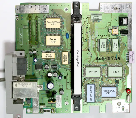
The SNES (or Super Famicom) does what it does by way of a combination of really going all in on direct memory access, and particularly having a dedicated setup for doing so between scanlines, coupled with a bunch of dedicated graphical modes specialized for different use cases, and you know, that you can switch between partway through drawing a screen. And of course the feature everyone knows and loves where you can have one polygon and do all sorts of fun things with it.
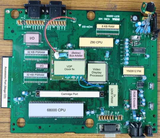
The Genesis (or Megadrive) has an actual proper 16-bit processor instead of this weird upgraded 6502 like the SNES had for a scrapped backwards compatibility plan. It also had this frankly wacky design where they just kinda took the guts out of a Sega Master System and had them off to the side as a segregated system whose only real job is managing the sound chip, one of those good good Yamaha synths with that real distinct sound... oh and they also actually did have a backwards compatibility deal that just kinda used the audio side to emulate an SMS, basically.
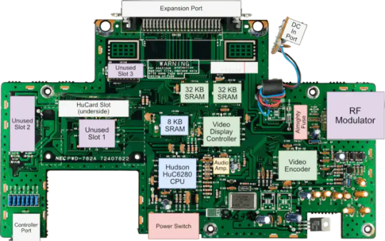
The TurboGrafix-16 (or PC Engine) really just kinda went all-in on making its own custom CPU from scratch which...we'll get to that, and otherwise uh... it had some interesting stuff going on sound wise? I feel like the main thing it had going was getting in on CDs early but I'm not messing with optical drives and they're no longer a really great storage option anyway.
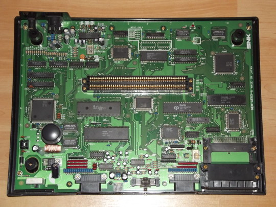
Then there's the Neo Geo... where what's going on under the good is just kind of A LOT. I don't have the same handy analysis ready to go on this one, but my understanding is it didn't really go in for a lot of nice streamlining tricks and just kinda powered through. Like it has no separation of background layers and sprites. It's just all sprites. Shove those raw numbers.
So what's the best of all worlds option here? I'd like to go with one of them nice speedy Motorolla processors. The 68000 the Genesis used is no longer manufactured though. The closest still-in-production equivalent would be the 68SEC000 family. Seems like they go for about $15 a pop, have a full 32-bit bus, low voltage, some support clock speeds like... three times what the Genesis did. It's overkill, but should remove any concerns I have about having a way higher resolution than the systems I'm jumping off from. I can also easily throw in some beefy RAM chips where I need.
I was also planning to just directly replicate the Genesis sound setup, weird as it is, but hit the slight hiccup that the Z80 was JUST discontinued, like a month or two ago. Pretty sure someone already has a clone of it, might use that.
Here's where everything comes to a screeching halt though. While the makers of all these systems were making contracts for custom processors to add a couple extra features in that I should be able to work around by just using newer descendant chips that have that built in, there really just is no off the shelf PPU that I'm aware of. EVERYONE back in the day had some custom ASIC (application-specific integrated circuit) chip made to assemble every frame of video before throwing it at the TV. Especially the SNES, with all its modes changing the logic there and the HDMA getting all up in those mode 7 effects. Which are again, something I definitely want to replicate here.
So one option here is... I design and order my own ASIC chips. I can probably just fit the entire system in one even? This however comes with two big problems. It's pricy. Real pricy. Don't think it's really practical if I'm not ordering in bulk and this is a project I assume has a really niche audience. Also, I mean, if I'm custom ordering a chip, I can't really rationalize having stuff I could cram in there for free sitting outside as separate costly chips, and hell, if it's all gonna be in one package I'm no longer making this an educational electronics kit/console, so I may as well just emulate the whole thing on like a raspberry pi for a tenth of the cost or something.
The other option is... I commit to even more work, and find a way to reverse engineer all the functionality I want out with some big array of custom ROMs and placeholder RAM and just kinda have my own multi-chip homebrew co-processors? Still PROBABLY cheaper than the ASIC solution and I guess not really making more research work for myself. It's just going to make for a bigger/more crowded motherboard or something.
Oh and I'm now looking at a 5V processor and making controllers compatible with a 10V system so I need to double check that all the components in those don't really care that much and maybe adjust things.
And then there's also FPGAs (field programmable gate arrays). Even more expensive than an ASIC, but the advantage is it's sort of a chip emulator and you can reflash it with something else. So if you're specifically in the MiSTer scene, I just host a file somewhere and you make the one you already have pretend to be this system. So... good news for those people but I still need to actually build something here.
So... yeah that's where all this stands right now. I admit I'm in way way over my head, but I should get somewhere eventually?
11 notes
·
View notes
Text
HDI PCB vs. Traditional Multilayer PCB: What’s the Difference?
As electronic products continue to shrink in size and increase in functionality, designers are faced with new challenges in PCB layout and integration. Two common solutions are Traditional Multilayer PCBs and HDI (High-Density Interconnect) PCBs. Though they serve similar purposes, they differ significantly in design approach, manufacturing complexity, and application scope.
What is a Traditional Multilayer PCB?
A traditional multilayer PCB consists of three or more conductive layers, typically stacked symmetrically with insulating materials (prepreg and core) in between. These boards use through-hole vias to connect all layers and are widely used in industrial, automotive, and consumer electronics.
Standard via types: Through-hole
Layer count: Usually 4–12 layers
Trace width & spacing: Limited by mechanical drilling
Common applications: Power supplies, industrial controllers, communication modules
What is an HDI PCB?
HDI (High-Density Interconnect) PCBs are a more advanced type of multilayer board designed for higher wiring density in a smaller footprint. HDI boards make use of microvias, blind/buried vias, and via-in-pad technologies to achieve compact layouts.
Advanced via types: Microvias, blind vias, buried vias
Layer count: Often 6–20+, including build-up layers
Trace width & spacing: Much finer (can be below 75μm)
Common applications: Smartphones, tablets, medical devices, aerospace electronics
Key Differences
1. Via Technology
Traditional multilayer PCBs rely mainly on mechanical drilling and through-hole vias, which limit routing density.
HDI PCBs use laser-drilled microvias that connect only adjacent layers, allowing finer routing and stacked via structures.
2. Density and Miniaturization
HDI allows more interconnections per unit area, which supports smaller components (e.g., BGAs with 0.4mm pitch).
Traditional PCBs are less suitable for extremely compact or high-pin-count layouts.
3. Manufacturing Complexity
HDI fabrication requires advanced processes like laser drilling, sequential lamination, and high-precision registration.
Traditional multilayer boards follow a simpler, more mature process and are easier to produce in volume.
4. Cost
HDI boards are generally more expensive due to complex manufacturing and tighter tolerances.
Traditional multilayer PCBs are more cost-effective for larger, less space-constrained designs.
5. Signal Integrity
HDI offers shorter trace lengths and better impedance control, making it suitable for high-speed digital and RF signals.
Traditional boards may struggle with signal integrity at very high frequencies.
When to Use HDI or Traditional Multilayer?
Choose HDI PCB when:
Space is extremely limited (e.g., wearables, smartphones)
High-speed or high-frequency signals are involved
You need finer pitch components (e.g., CPU, GPU, DDR)
You aim for thinner, lighter, more compact devices
Choose Traditional Multilayer PCB when:
Size and weight are less critical
The design uses standard components and moderate speeds
Cost is a major concern
Volume production and fast lead time are priorities
Conclusion
Both HDI and traditional multilayer PCBs play important roles in modern electronics. The right choice depends on your application’s complexity, space constraints, performance requirements, and budget. HDI pushes the limits of miniaturization and performance, while traditional multilayer PCBs remain a reliable and economical solution for many mainstream applications.

0 notes
Text
How to Choose the Right Manual Fixture for Your Testing Needs: A Step-by-Step Guide
In the world of electronics testing and precision manufacturing, the right tools can make the difference between flawless performance and costly rework. Among those tools, the manual fixture plays a pivotal yet often underrated role in ensuring quality, consistency, and efficiency. Whether you're testing PCBs, wiring harnesses, or microelectronic components, selecting the ideal manual fixture is crucial for optimizing test results and minimizing downtime.
But with countless configurations, materials, and functions available, how do you determine which fixture is best suited for your testing environment?
In this guide, we’ll break down the key steps and considerations to help you choose the perfect manual fixture for your specific needs—whether you’re a test engineer, production manager, or quality control specialist.
Step 1: Define Your Testing Objectives Clearly
Before exploring fixture options, clarify what you want the fixture to accomplish. Are you focused on functional testing, continuity testing, or high-voltage isolation? Will it be used in a high-volume production environment or for prototype verification?
Understanding your goals will help narrow down the required features, such as:
Contact type (spring-loaded pins, pogo pins, etc.)
Force requirements
Number of test points
Load/unload speed
At Equip-Test, manual fixture solutions are available for everything from standard bed-of-nails setups to fully customized designs tailored to specific PCB layouts and test flows.
Step 2: Assess the Component or Board Geometry
Next, evaluate the physical characteristics of the unit under test (UUT):
What are the dimensions of the board or component?
Are there connectors or edge contacts?
Does the test require double-sided probing?
These factors will influence the fixture’s platform size, the arrangement of test probes, and whether a top-side pressure plate or vacuum hold-down is necessary.
Equip-Test offers both standard and modular manual fixture systems, making it easier to accommodate complex board geometries without reinventing the wheel every time.
Step 3: Choose the Right Probing Technology
One of the most critical aspects of a manual fixture is the selection of test probes. Depending on the signal integrity, current rating, and pitch requirements, you might need:
Standard spring-loaded probes for through-hole or SMT pads
High-frequency probes for RF circuits
Kelvin probes for low-resistance measurements
Special probes for surface wear or sensitive contacts
Don’t overlook the importance of probe life cycle and accessibility, especially in high-throughput environments.
Equip-Test's vast test probe catalog is engineered to support virtually every test scenario imaginable, ensuring precision and durability.
Step 4: Factor in Ergonomics and Operator Safety
Manual fixtures should not only be functional but also comfortable and safe to use. Consider:
Lever mechanisms or pneumatic assist for high-contact-count boards
Clear visibility and easy access to the DUT
Built-in ESD protection
Shielding for high-voltage applications
A poorly designed manual fixture can increase operator fatigue and error rates. Ergonomic enhancements also reduce the risk of repetitive strain injuries during continuous operation.
Step 5: Plan for Scalability and Maintenance
If your test needs might change in the near future, it’s wise to invest in a modular or upgradable fixture. Look for designs that allow:
Easy probe replacement
Interchangeable probe plates
Quick fixture swaps for different board versions
This is where modular fixture platforms from Equip-Test really shine. These fixtures can be easily reconfigured or upgraded, providing flexibility without excessive downtime or new tooling costs.
Step 6: Work with a Trusted Fixture Manufacturer
Even with a clear checklist, designing the perfect fixture isn’t always DIY-friendly. Partnering with a company that specializes in test fixture development ensures:
Optimal layout and mechanical design
High-quality materials and build
Fast turnaround and support for modifications
Integration with test equipment (ICT, functional testers, etc.)
Equip-Test has been at the forefront of manual fixture solutions for years, supporting global electronics manufacturers with robust, reliable test platforms. Whether you're outfitting a new production line or upgrading legacy systems, their engineering team brings unmatched expertise to every custom fixture build.
Final Thoughts: Precision Starts at the Fixture
Your test equipment is only as good as the connection it makes with the unit under test—and that connection starts with a well-chosen manual fixture. By carefully considering your application requirements, board design, probe technology, ergonomics, and future needs, you can ensure accurate, repeatable test results while keeping costs under control.
Ready to explore your options or need expert advice? Visit Equip-Test to discover high-performance manual fixtures designed to elevate your testing process from the ground up.
0 notes
Text
What is a PCB Footprint? 5 Things to Know About PCB Footprints
5 Things to Know About PCB Footprints
The process of putting together a printed circuit board is not an easy task. From PCB designing to assembly, different details are involved. Along with this amalgamation of different components, the process of PCB footprint is also a crucial task. In this process, electrical points and physical layouts are allocated to the various elements mounted on a PCB board.
To put it in simple terms, PCB footprints refer to the area that the different components occupy on a printed circuit board. From the pad size and shape to the component outline, all the things come under PCB footprints. This blog will provide various insights into PCB footprints.
1. Information on the Components of PCB Footprints
A circuit board design components come with general information, which are:
Pads: This indicates copper areas where the component leads or pins will be soldered during the assembly process.
Component outline: The area that the components occupy on the PCB is the outline or courtyard. This boundary defines the component shape.
Reference designator: In the PCB layout, you can witness alphanumeric codes. These codes identify the components on the PCB.
2. Libraries for PCB Footprints
An enthusiastic PCB designer would know how important it is to create a PCB footprint library just like its component library. Generally, PCB footprint libraries are available to organizations that are Component manufacturers, third parties, or those who create design software for printed circuit boards. There are various PCB footprints available online. The most popular of them are SnapEDA and Ultra Librarian. The Ultra Librarian is considered to be the world’s largest PCB CAD library. The data of this library can be imported into well-known PCB CAD apps.
3. PCB Footprint Creation
If a PCB footprint library is not available, PCB designers will not have any other choice but to create a PCB footprint on their own. Later, they will upload it to the PCB library database. To create a PCB footprint from scratch, it is essential to have the correct specifications of the concerned components. Start with the general information like pad sizes, hole diameter, pitch and spacing, the component layouts, etc. Ensure the PCB footprint creation is complete otherwise, it can cause problems when you have to define the PCB layout.
4. Specific Standards
To define the PCB layout, its schematic symbol, or 3D model, the PCB footprint should apply to specific international standards:
For PCB footprint, the standard is IPC 7351. The IPC-SM-7351-B version of this standard considers a range of formulas to define the footprint. Many PCB CAD models have been designed, aligning with this standard.
For schematic symbols, the standard is ANSI Y32.2-1975. In electronic and electrical diagrams, certain graphic symbols and designated letters are used. This standard is used to define such elements.
For 3D models, ISO 10303-21 is used. This standard classifies the STEP model file format.
5. Guidelines for PCB Footprints
If a PCB designer wants to create the footprint from the beginning, individuals should follow the guidelines mentioned below:
The component layout on the PCB should be aligned perfectly. The pads of the components on opposite sides should be of similar shapes and sizes to ensure symmetry.
The component outline and the pads should have enough space in between. This would make sure that the desired pins are connected to the right component pads.
To indicate polarized components, integrate polarity indicators.
Don’t use components that are too small, as the automated production process may fail to recognize those parts.
Conclusion
During the PCB manufacturing process, PCB footprints play a crucial role. They contain information about all the components mounted on the PCB layout. By going through the essential set of information, the soldering process can be done accurately. Usually, PCB footprints are available online, but if a designer wants to create it from scratch, they can do so by following the guidelines.
Frequently Asked Questions:
What is a PCB footprint in PCB design?
A PCB footprint is the physical layout of a component on a circuit board, including pad positions, outlines, and reference markings for accurate placement and soldering.
Why are PCB footprints important?
PCB footprints ensure correct component placement, prevent assembly errors, and improve PCB reliability by following industry standards like IPC 7351.
How do I create a PCB footprint?
PCB footprints can be created using PCB design software by defining pad sizes, hole spacing, and component outlines, or downloaded from libraries like SnapEDA or Ultra Librarian.
What are the best practices for PCB footprint design?
Ensure correct pad alignment, spacing, and polarity marking, and follow IPC standards to avoid soldering defects and improve manufacturability.
Know More: https://www.pcbpower.us/blog/what-is-a-pcb-footprint
0 notes
Text
How to make golden finger PCB
Gold Finger is a row of gold-plated conductive contacts designed on the edge of a printed circuit board (PCB), named after their surface being gold-plated and resembling fingers. It is the physical interface that enables electrical connection between PCB and other devices such as motherboard slots, expansion card interfaces, etc.So,how to make golden fingers PCB?
1. Structural design of golden fingers
-Oblique (guide angle) design
The edge of the golden finger should be designed at 45 ° or other angles (such as 20 °, 30 °) to reduce friction damage when inserted into the slot. If not chamfered, the right angle is prone to scratching the slot, reducing reliability.
-Safe distance
The golden finger should maintain a safe distance of 0.6-1.5mm from the edge of the board to prevent damage to the coating during beveled edge treatment. The thickness range of the board is usually 1.2-2.4mm, and if it exceeds this range, it may not be possible to beveled it.
-Layout of long and short gold fingers
Main lead width of 40mil, secondary lead width of 20mil, connection points of 6mil, spacing of 8mil. When the leads enter the single board, they need to be connected diagonally or with rounded corners to avoid impedance jumps caused by right angles.
2. Electrical and solder mask design of Golden Finger
-Solder mask window
The golden finger area needs to be completely opened to avoid poor contact caused by solder mask ink residue. The window opening range should be 10mm larger than the edge of the board and kept at a distance from the surrounding copper skin to prevent copper exposure.
-Restrictions on surface copper plating
Copper plating is prohibited on the surface of the gold finger to avoid multiple identical network solder pads being connected as a whole, which may affect insertion and removal.
-Inner layer copper cutting treatment
The inner layer needs to be copper cut by at least 3mm to reduce the impedance difference between the gold finger and the impedance line, while enhancing ESD protection capability. Some designs (such as PCIe) require full copper cutting in the gold finger area.
3. Material and Coating Selection
-Electroplated hard gold
Thickness 3-50 μ m, containing nickel/cobalt alloy, high hardness (200+HV), strong wear resistance, suitable for high-frequency plugging scenarios (such as graphics cards, industrial equipment), but with high cost.
-Chemical immersion gold (ENIG)
thickness 1-3 μ m, smooth surface, low cost, suitable for low insertion and extraction frequency scenarios (such as consumer grade memory), but poor wear resistance.
---
The manufacturing process of golden fingers, how to make golden fingers?
1. Core process flow of Golden Finger
-Substrate treatment: Copper substrates are etched to form conductive contacts, followed by nickel plating as the bottom layer to improve adhesion and corrosion resistance.
-Gold plating process:
-Electroplating hard gold: By electrolytically depositing gold cobalt/gold nickel alloy, the thickness is controllable and suitable for local high wear resistance requirements.
-Chemical deposition of gold: forming a uniform gold layer through non current deposition, low cost, suitable for whole board processing.
-Diagonal cutting: precise guide angles are achieved using CNC milling machines or laser cutting, typically ranging from 20 ° to 45 °.
2. Special process requirements
-CAM compensation: The inner copper foil needs to be stacked according to the product type (80mil for ordinary products, 40mil for optoelectronic/memory products), with a lead width of 12mil and strict calibration of solder pad spacing.
-Anti oxidation treatment: Before gold plating, the copper surface needs to be thoroughly cleaned, and some processes introduce nitrogen gas protection to prevent oxidation.
---
Key considerations in the manufacturing process of golden fingers
1. Process control
-Consistency of plating thickness: When electroplating hard gold, it is necessary to ensure uniform thickness and avoid local thinning that may cause a decrease in wear resistance.
-Drilling accuracy: The aperture and depth should be consistent to avoid interference or damage to the PCB during insertion and removal.
2. Quality control
-Wear resistance test: High frequency insertion and extraction scenarios (such as PCIe) require ≥ 500 insertion and extraction tests to ensure that the coating does not peel off.
-DFM detection: Use tools such as Huaqiu DFM to detect design files in advance and avoid production risks. The cost of gold finger products is high, and it is necessary to strictly avoid rework of finished products.
3. Environment and operating standards
-Pollution prevention: It is forbidden to directly touch the golden fingers during operation to avoid surface contamination by oil or impurities.
-Storage and transportation: shockproof packaging is required to avoid damage to the coating caused by mechanical impact.
---
Comparison and Trends
-Alternative solution: Gold finger tin plating/silver has low cost but short lifespan; Emerging high-density connectors (such as LCP materials) are gradually being applied, but gold fingers still dominate the field of high reliability.
-Environmental trend: In the future, lead-free electroplating or renewable materials may be used to reduce environmental impact.
By optimizing design and process control, Goldfinger continues to play a critical role in high-frequency, high reliability electronic devices such as 5G and AI hardware.
0 notes
Text
Circuit Card Assembly Experts – Fast, Reliable & Precise
The demand for high-quality Circuit Card Assembly (CCA) and PCB manufacturing services has reached unprecedented levels. From cutting-edge consumer electronics and life-saving medical devices to robust industrial automation systems and next-generation aerospace technology, every industry relies on precision-engineered printed circuit boards to power their innovations.
Choosing the right PCB manufacturing company isn’t just about getting boards assembled—it’s about ensuring performance, durability, and reliability at every stage of production. Whether you're a startup developing a breakthrough IoT device or a Fortune 500 company scaling up production, partnering with expert Circuit Card Assembly manufacturers can make the difference between a product that excels and one that falls short.
Why Choose Expert Circuit Card Assembly Services?
When it comes to PCB manufacturing and assembly, precision, speed, and dependability are crucial. Here’s why working with Circuit Card Assembly experts makes all the difference:
Fast Turnaround Without Compromising Quality
Time-to-market is critical in electronics manufacturing. A professional PCB manufacturing assembly provider uses advanced machinery and streamlined processes to deliver quick turnarounds without sacrificing quality. Whether you need prototype assemblies or high-volume production, expert manufacturers ensure your boards are assembled efficiently.
Reliable & Consistent Performance
A defective PCB can lead to costly delays and product failures. Reputable Circuit Card Assembly manufacturers implement strict quality control measures, including automated optical inspection (AOI), X-ray testing, and functional testing, to ensure every board performs flawlessly. This reliability is essential for industries like aerospace, automotive, and medical devices, where failure is not an option.
Precision Engineering for Complex Designs
Modern electronics require intricate PCB designs with high-density components, fine-pitch soldering, and multi-layer configurations. Skilled Circuit Card Assembly experts leverage cutting-edge technology like surface-mount technology (SMT) and through-hole assembly to handle even the most complex designs with accuracy.
End-to-End PCB Manufacturing Solutions
Leading PCB manufacturing companies offer comprehensive services, including:
Design & Prototyping – Helping refine your PCB layout for optimal performance.
Component Sourcing – Procuring high-quality parts from trusted suppliers.
Assembly & Testing – Ensuring each board meets industry standards.
Box Build & Final Integration – Delivering fully assembled electronic systems.
This end-to-end approach simplifies production, reduces supply chain risks, and ensures consistency.
Compliance with Industry Standards
Certified PCB manufacturing assembly providers adhere to international standards such as ISO, IPC, and RoHS, guaranteeing that your products meet regulatory and safety requirements. This is especially important for industries with strict compliance needs, such as medical and military applications.
Choosing the Right PCB Manufacturing Partner
When selecting a Circuit Card Assembly manufacturer, consider:
Experience & Expertise – Look for a company with a proven track record in your industry.
Advanced Technology – Ensure they use the latest assembly and testing equipment.
Scalability – Can they handle both small and large production runs?
Customer Support – A responsive team ensures smooth communication and quick issue resolution.
Conclusion
For businesses seeking fast, reliable, and precise Circuit Card Assembly, partnering with an expert PCB manufacturing company is essential. From rapid prototyping to full-scale production, the right manufacturer ensures high-quality, high-performance PCBs that drive innovation and success.
Whether you're a startup or an established enterprise, investing in professional PCB manufacturing and assembly services guarantees efficiency, reliability, and a competitive edge in the electronics market. Choose wisely, and let the experts bring your designs to life!
0 notes
Text
LDO Voltage Regulators and Their PCB Design Challenges
Low Dropout (LDO) voltage regulators are key components in devices that require precise, low-noise power for sensitive circuits. Unlike traditional voltage regulators, LDOs operate efficiently even when the input voltage is close to the output voltage. These characteristics make them ideal for use in devices such as IoT sensors, wearables, and audio equipment, where clean and stable voltage is crucial.
What Are LDO Voltage Regulators?
LDO voltage regulators are a type of linear regulator that maintains a stable output voltage even when the input voltage is just slightly higher than the output voltage. This feature, known as the dropout voltage, is much smaller compared to traditional linear regulators. LDOs are ideal for systems where power loss needs to be minimized, and they are widely used in battery-operated devices.
Role of LDOs in PCB Design
LDO voltage regulators, though efficient, still require precise integration in PCBs to ensure optimal performance:
Noise Reduction: LDO regulators are used in analog circuits where noise minimization is essential. The output voltage needs to be as clean as possible, so careful filtering and capacitor selection are crucial to maintaining performance. Poor filtering can lead to unwanted ripple and noise that may affect the functionality of sensitive components.
Thermal Management: Even though LDOs are more efficient than traditional linear regulators, they still generate heat, particularly when there is a significant difference between the input and output voltages. Managing the heat dissipation through PCB layout, heat sinks, and thermal vias is critical to prevent overheating and ensure continuous operation.
Capacitor Selection: The selection of input and output capacitors is vital for ensuring the stability and efficiency of LDO voltage regulators. Capacitors with low equivalent series resistance (ESR) are often used in conjunction with LDOs to maintain a stable output and reduce ripple.
PCB Layout Considerations: To ensure proper LDO operation, designers must minimize the resistance and inductance in the PCB traces. This includes minimizing the distance between the LDO and its input and output capacitors and ensuring proper grounding techniques to reduce noise and voltage fluctuations.
Highleap Electronics and LDO PCB Manufacturing
Highleap Electronics offers high-quality PCB manufacturing and assembly services for LDO voltage regulators, ensuring that they meet the highest standards of performance and efficiency. Their experienced team ensures that every aspect of LDO integration—from thermal management to noise reduction and efficient component selection—is carefully handled. With fast-turnaround prototyping and batch production capabilities, Highleap Electronics provides reliable, cost-effective solutions for manufacturers in need of LDO voltage regulator PCBs.
For companies looking to design and manufacture LDO-based PCBs, Highleap Electronics offers tailored solutions that meet exacting requirements, with a commitment to quality and timely delivery. To learn more, visit https://hilelectronic.com/ and get in touch with their team to start your next project.
0 notes
Text
Tips for PCB Stackup Layout
With the continuous emergence of high-speed circuits, the complexity of PCB boards is also getting higher and higher. In order to avoid the interference of electrical factors, the signal plane and the power supply layer must be separated, so it involves the design of multilayer PCB, that is, the design of laminated structure.
1. Avoid Direct Connection of Two Signal Planes
In a multilayer PCB, it usually includes a signal plane (S), a power plane (P) plane and a ground plane (GND). How are the three arranged?
Power and ground planes are usually undivided solid planes that provide a good, low-impedance current return path for current from adjacent signal traces. Therefore, the signal plane is mostly adjacent to the power plane or the ground plane. Moreover, the power supply layer and ground plane use a large area of copper (so the power supply layer and ground plane are also called copper layer), and the large copper film can provide shielding for the signal plane, which is conducive to impedance control and improvement of signal quality.
In addition, should try to avoid two signal planes directly adjacent to each other. Crosstalk is easily introduced between adjacent signal planes, resulting in circuit failure. Adding a ground plane between the two signal planes can effectively avoid crosstalk.
2. Most Top and Bottom Planes are Signal Planes
The top and bottom planes of a multilayer PCB are usually used to place components and a small number of traces, so they are mostly signal planes. Generally, the top plane is the component, and the bottom plane (the second plane) of the component can be set as the ground plane, providing the device shielding layer and providing the reference plane for the top plane wiring.
In addition, note that these signal traces on the top and bottom planes cannot be too long to reduce direct radiation from the traces.
3.Reference Plane Preferred the Ground Plane
Both the power plane and the ground plane can be used as reference planes and have a certain shielding effect.
The difference between the two is that: the power supply layer has a high characteristic impedance, and there is a large potential difference with the reference level; while the ground plane is generally grounded and used as a reference point for the reference level, its shielding effect is much better than that of the power supply layer.
Therefore, when choosing a reference plane, the stratum is preferred.
4. The High-speed Signal Layer is Located in the Middle Plane of the Signal
The high-speed signal transmission layer in the circuit should be the signal intermediate plane and sandwiched between two copper layers. In this way, the copper film of the two copper layers can provide electromagnetic shielding for high-speed signal transmission, and at the same time, it can effectively limit the radiation of the high-speed signal between the two copper layers without causing external interference.
5.The Power Plane and the Ground Plane are Preferably Paired
The power supply layer and the ground plane appear in pairs, shortening the distance between the power supply and the ground plane can reduce the impedance of the power supply, which is beneficial to the stability of the power supply and reducing EMI. In particular, the main power supply should be as adjacent to its corresponding ground plane as possible. In the case of high speed, you can add extra ground planes to isolate the signal plane, but it is recommended not to add more power planes to isolate, because the power plane will bring more high-frequency noise interference.
6.Copper Layer Balance Design
The copper layer, that is, the power plane or the ground plane, is best arranged symmetrically, such as the second plane and the fifth layer of the 6-layer board, or the third layer and the fourth layer should be copper-plated together, which is considered to be flat and horizontal in the process. Structural requirements, as unbalanced copper layers may cause warpage as the PCB expands.
7.Multiple Power Planes away from High-speed Signal Planes
Multiple power supply layers should be kept away from high-speed digital signal wiring. Because the multi-power supply layer will be divided into several physical regions with different voltages, if the signal power is close to the multi-power supply layer, the signal current on the nearby signal layer will encounter an unsatisfactory return path, making the return path A gap appears.
8.Use Even-numbered layers
The classic PCB stack-up design is almost entirely even-numbered, not odd-numbered. Even-numbered layers of printed circuit boards have cost advantages, and even-numbered layers are more resistant to board warpage than odd-numbered layers.
9.Arrange Routing on Adjacent Layers
In order to complete complex wiring, the transition between layers of traces is inevitable. The two layers spanned by a signal path are called a "routing combination". The best routing combination design is to avoid return current flow from one reference plane to another reference plane, but rather to flow from one point (surface) of one reference plane to another point (surface).
Therefore, wiring combinations are preferably arranged on adjacent layers, because a path through multilayers is not clear for return currents. Although the ground bounce can be reduced by placing decoupling capacitors near the vias or reducing the thickness of the dielectric between the reference planes, it is not a good design.
10.The Routing Directions of Adjacent Signal Planes are Orthogonal
On the same signal plane, the direction of most wiring should be consistent, and it should be orthogonal to the wiring direction of adjacent signal planes. For example, the wiring direction of one signal plane may be set to the "Y-axis" direction, and the wiring direction of another adjacent signal plane may be set to the "X-axis" direction.
On the other hand, how to do impedance control is a headache for many users, but Hitech Circuits makes everything so easy. Hitech Circuits will automatically calculate the line width and line spacing corresponding to different impedance controls according to different stacks, so as to do impedance matching for the user, without the need to perform complex impedance calculations manually, saving effort and worry!
0 notes
Text
Electronic Product Designer vs. Industrial Product Designer: Key Differences Explained
The lines between electronic and industrial design often blur. While both fields involve creating tangible products, they have distinct focuses and skill sets. Understanding the key differences between an electronic and industrial product designer can help you navigate the complex landscape of product development.

Electronic Product Designer
An electronic product designer is primarily concerned with the internal workings of a device. They focus on electrical and electronic components, circuit design, and software integration. Their goal is to ensure the product functions efficiently and reliably.
Key Responsibilities of an Electronic Product Designer:
Circuit Design: Designing and simulating electronic circuits, including analog and digital circuits.
Component Selection: Choosing appropriate electronic components, considering factors like cost, performance, and availability.
PCB Layout: Designing printed circuit boards (PCBs) to efficiently route electrical signals and power.
Firmware Development: Writing firmware to control the device's hardware and software interactions.
Testing and Debugging: Identifying and resolving issues in the product's electronic systems.
Industrial Product Designer
In contrast, an industrial product designer concentrates on a product's outward look and user experience. They take into account things like production viability, ergonomics, and aesthetics. Their goal is to create products that are not only practical but also visually beautiful and easy to use.
Key Responsibilities of an Industrial Product Designer:
Conceptual Design: Generating initial ideas and concepts for the product's form and function.
Sketching and Modeling: Creating 2D and 3D models to visualize the product's design.
User Interface (UI) and User Experience (UX) Design: Designing the user interface and ensuring a seamless user experience.
Manufacturing Considerations: Collaborating with engineers to ensure the product is manufacturable and cost-effective.
The Overlap
While electronic and industrial design have distinct focuses, they often intersect. For example, an electronic product designer might collaborate with an industrial designer to ensure that the device's internal components are accessible for repair or upgrade. Similarly, an industrial designer might need to understand the technical constraints of a product to create a design that is both aesthetically pleasing and functional.
Both electronic and industrial product designers play crucial roles in bringing products to market. By understanding their unique strengths and how they complement each other, we can create innovative and user-friendly products that meet the demands of today's consumers.
Source: https://extrondesignservice.blogspot.com/2024/12/electronic-product-designer-vs.html
0 notes
Text
FCBGA Substrate: Understanding Its Importance in Electronic Manufacturing
What is an FCBGA Substrate?
FCBGA (Flip-Chip Ball Grid Array) is an advanced packaging technology used for encapsulating electronic chips. This packaging technique involves flipping the chip (flip-chip) and connecting it to the substrate through a grid of solder balls (Ball Grid Array). The FCBGA substrate is a critical component that provides support, thermal management, and electrical connections. It is typically used for high-performance microprocessors, graphics processing units (GPUs), and other chips that require high-speed signal transmission and high-density packaging.
How FCBGA Works
FCBGA packaging works by flipping the chip and connecting its pins to the substrate through tiny solder balls in a grid formation. This method differs from traditional packaging methods, such as QFP (Quad Flat Package) or BGA (Ball Grid Array), which use pins or pin arrays for connection, whereas FCBGA directly connects through solder balls.
The role of the FCBGA substrate is to provide mechanical support and electrical contact. The design of the substrate needs to ensure a high-density ball array layout and excellent thermal conductivity to handle the heat dissipation demands of high-power, high-frequency chips.
Structure of FCBGA Substrate
The design of an FCBGA substrate is complex and typically consists of multiple layers. The main layers include:
Chip Bonding Layer: This layer sits between the chip and the substrate, where solder balls are used to connect the chip’s pads to the substrate’s circuits. The solder balls are typically made from an alloy of tin and other metals, offering good electrical conductivity and thermal properties.
Circuit Layer: The circuit layer transmits electrical signals and is usually made of copper. These layers are created using multi-layer printed circuit board (PCB) technology. The layout and density of these layers are crucial for signal integrity and minimizing crosstalk.
Package Substrate: The package substrate serves as the foundation for the entire FCBGA package. It is typically made of materials like ceramics or glass fiber-reinforced epoxy resin (FR4). This layer provides structural support and ensures good connectivity between the solder balls and external circuit boards.
Heat Dissipation Layer: For high-power chips, heat management is crucial. FCBGA substrates often incorporate heat dissipation layers made of copper or other high thermal conductivity materials. These layers help transfer heat from the chip to the external environment, preventing overheating and chip damage.
Testing and Encapsulation Layer: During the manufacturing process, the FCBGA package undergoes extensive testing to ensure each package works as expected. The encapsulation layer is usually made of polymer materials and serves to protect the chip while adding mechanical strength to the package.
Advantages of FCBGA Substrate
FCBGA substrates offer many advantages due to their unique design and material choices. These benefits are especially apparent in high-performance and high-density electronic devices. Here are some of the key advantages:
High-Density Interconnects (HDI): The flip-chip design and ball grid array layout support extremely high interconnect densities. The circuit lines on the substrate can be packed more tightly, reducing the package size while enhancing electrical performance.
Excellent Thermal Management: FCBGA substrates excel in thermal management, effectively transferring heat from the chip. Since high-power chips generate a lot of heat, effective thermal design is essential to ensure reliable chip performance and longevity.
Smaller Package Size: FCBGA packages are typically smaller than traditional packages, making them ideal for applications where space is limited. This compact design allows for the integration of more functions into devices like high-end smartphones, servers, and portable electronics without increasing their size.
High-Speed Signal Transmission: The flip-chip design reduces the signal transmission path length, allowing for faster data transfer speeds. This feature is crucial for applications that require high-speed computation, such as processors and graphics chips.
Improved Reliability: The solder ball connection method used in FCBGA packages is more reliable than traditional pin-based connections. It can withstand higher mechanical stresses and temperature fluctuations, making it ideal for high-reliability applications.
Applications of FCBGA Substrate
FCBGA substrates are used across a wide range of electronic products, particularly in industries where high performance, high density, and high reliability are required. Some of the key applications include:
Central Processing Units (CPUs) and Graphics Processing Units (GPUs): FCBGA packaging is commonly used for high-performance computing chips like CPUs and GPUs, which require high processing power and effective heat management. The FCBGA substrate provides the necessary high-density connections and thermal dissipation needed for these chips to run efficiently at higher speeds and lower temperatures.
Servers and Data Centers: Processors used in servers and data centers need to handle large amounts of data, making their packaging requirements extremely demanding. FCBGA substrates' high-density interconnects and excellent thermal performance make them ideal for data center processors.
Mobile Devices: Processors and graphics chips in smartphones, tablets, and other mobile devices also utilize FCBGA packaging. The compact nature and efficient thermal management of FCBGA substrates are particularly suited for mobile devices that face size constraints.
Automotive Electronics: FCBGA substrates are also used in automotive electronics, such as self-driving, in-car entertainment systems, and electric vehicle control units. Automotive electronics must perform reliably in harsh environments, making the high durability and thermal management capabilities of FCBGA packaging a perfect fit.
Challenges and Future of FCBGA
While FCBGA substrates offer significant advantages, they also face some challenges:
Manufacturing Cost: The manufacturing process for FCBGA substrates is complex, involving precise fabrication and material selection, which increases the cost compared to traditional packaging methods. This could limit its use in lower-end products.
Thermal Issues: Although FCBGA substrates have good thermal management, as chip power increases, managing heat dissipation remains a challenge. Finding the balance between high-power density and effective cooling continues to be a key focus of packaging research.
Signal Integrity: High-speed signal transmission presents a challenge for FCBGA packaging. As chip frequencies increase, ensuring signal integrity and minimizing signal interference become critical issues in the design process.
FCBGA substrates are a crucial component in modern electronic packaging, offering high density, performance, and reliability. They are widely used in processors, GPUs, servers, mobile devices, and automotive electronics. As electronic devices continue to evolve and demand higher performance, FCBGA packaging will remain an essential technology.
The future of FCBGA substrates lies in overcoming challenges such as cost, thermal management, and signal integrity while pushing the boundaries of chip performance and miniaturization. With continuous advancements in packaging technology, FCBGA substrates will play a vital role in the next generation of high-performance electronic devices.
1 note
·
View note
Text
How to Choose the Right Manual Fixture for Your Testing Needs: A Step-by-Step Guide
In the world of electronics testing and precision manufacturing, the right tools can make the difference between flawless performance and costly rework. Among those tools, the manual fixture plays a pivotal yet often underrated role in ensuring quality, consistency, and efficiency. Whether you're testing PCBs, wiring harnesses, or microelectronic components, selecting the ideal manual fixture is crucial for optimizing test results and minimizing downtime.
But with countless configurations, materials, and functions available, how do you determine which fixture is best suited for your testing environment?
In this guide, we’ll break down the key steps and considerations to help you choose the perfect manual fixture for your specific needs—whether you’re a test engineer, production manager, or quality control specialist.
Step 1: Define Your Testing Objectives Clearly
Before exploring fixture options, clarify what you want the fixture to accomplish. Are you focused on functional testing, continuity testing, or high-voltage isolation? Will it be used in a high-volume production environment or for prototype verification?
Understanding your goals will help narrow down the required features, such as:
Contact type (spring-loaded pins, pogo pins, etc.)
Force requirements
Number of test points
Load/unload speed
At Equip-Test, manual fixture solutions are available for everything from standard bed-of-nails setups to fully customized designs tailored to specific PCB layouts and test flows.
Step 2: Assess the Component or Board Geometry
Next, evaluate the physical characteristics of the unit under test (UUT):
What are the dimensions of the board or component?
Are there connectors or edge contacts?
Does the test require double-sided probing?
These factors will influence the fixture’s platform size, the arrangement of test probes, and whether a top-side pressure plate or vacuum hold-down is necessary.
Equip-Test offers both standard and modular manual fixture systems, making it easier to accommodate complex board geometries without reinventing the wheel every time.
Step 3: Choose the Right Probing Technology
One of the most critical aspects of a manual fixture is the selection of test probes. Depending on the signal integrity, current rating, and pitch requirements, you might need:
Standard spring-loaded probes for through-hole or SMT pads
High-frequency probes for RF circuits
Kelvin probes for low-resistance measurements
Special probes for surface wear or sensitive contacts
Don’t overlook the importance of probe life cycle and accessibility, especially in high-throughput environments.
Equip-Test's vast test probe catalog is engineered to support virtually every test scenario imaginable, ensuring precision and durability.
Step 4: Factor in Ergonomics and Operator Safety
Manual fixtures should not only be functional but also comfortable and safe to use. Consider:
Lever mechanisms or pneumatic assist for high-contact-count boards
Clear visibility and easy access to the DUT
Built-in ESD protection
Shielding for high-voltage applications
A poorly designed manual fixture can increase operator fatigue and error rates. Ergonomic enhancements also reduce the risk of repetitive strain injuries during continuous operation.
Step 5: Plan for Scalability and Maintenance
If your test needs might change in the near future, it’s wise to invest in a modular or upgradable fixture. Look for designs that allow:
Easy probe replacement
Interchangeable probe plates
Quick fixture swaps for different board versions
This is where modular fixture platforms from Equip-Test really shine. These fixtures can be easily reconfigured or upgraded, providing flexibility without excessive downtime or new tooling costs.
Step 6: Work with a Trusted Fixture Manufacturer
Even with a clear checklist, designing the perfect fixture isn’t always DIY-friendly. Partnering with a company that specializes in test fixture development ensures:
Optimal layout and mechanical design
High-quality materials and build
Fast turnaround and support for modifications
Integration with test equipment (ICT, functional testers, etc.)
Equip-Test has been at the forefront of manual fixture solutions for years, supporting global electronics manufacturers with robust, reliable test platforms. Whether you're outfitting a new production line or upgrading legacy systems, their engineering team brings unmatched expertise to every custom fixture build.
Final Thoughts: Precision Starts at the Fixture
Your test equipment is only as good as the connection it makes with the unit under test—and that connection starts with a well-chosen manual fixture. By carefully considering your application requirements, board design, probe technology, ergonomics, and future needs, you can ensure accurate, repeatable test results while keeping costs under control.
Ready to explore your options or need expert advice? Visit Equip-Test to discover high-performance manual fixtures designed to elevate your testing process from the ground up.
0 notes
Text
The Evolution and Advantages of HDI PCB Fabrication in Modern Electronics
The Evolution and Advantages of HDI PCB Fabrication in Modern Electronics
High-Density Interconnect (HDI) Printed Circuit Boards (PCBs) represent a significant advancement in PCB technology, offering enhanced performance and miniaturization for modern electronic devices. As consumer demand for smaller, faster, and more powerful electronics continues to grow, HDI PCBs have become a critical component in meeting these requirements. This article explores the evolution, fabrication process, and advantages of HDI PCB fabrication, highlighting its impact on the electronics industry.Get more news about Hdi PCB fabrication,you can vist our website!
The Evolution of HDI PCBs The development of HDI PCBs has been driven by the need for increased functionality and reduced size in electronic devices. Traditional PCBs, while effective, have limitations in terms of layer count, component density, and signal integrity. HDI technology addresses these limitations by incorporating advanced design and manufacturing techniques that enable higher component density and improved electrical performance.
The evolution of HDI PCBs can be traced back to the 1980s when the first multi-layer PCBs were introduced. Since then, advancements in materials, fabrication methods, and design software have led to the creation of HDI PCBs with multiple layers, finer lines and spaces, and smaller via structures. Today, HDI technology is widely used in various industries, including consumer electronics, telecommunications, automotive, and aerospace.
The HDI PCB Fabrication Process The fabrication of HDI PCBs involves several key steps, each contributing to the overall performance and reliability of the final product:
Design and Layout
The fabrication process begins with the design and layout of the HDI PCB. Advanced design software is used to create detailed schematics and layouts that optimize the placement of components, vias, and traces. Designers must consider factors such as signal integrity, thermal management, and manufacturability during this phase.
Material Selection
The choice of materials is critical for the performance of HDI PCBs. High-quality laminates, copper foils, and prepregs are selected to ensure the board's durability, electrical performance, and thermal stability. The materials must also be compatible with the specific fabrication processes used for HDI PCBs.
Laser Drilling and Via Formation
One of the defining features of HDI PCBs is the use of microvias—small, high-density vias that connect different layers of the PCB. Laser drilling technology is employed to create these microvias with precision and accuracy. Blind, buried, and stacked vias are commonly used in HDI PCBs to achieve higher interconnect density and improved signal performance.
Layer Lamination
The individual layers of the HDI PCB are laminated together using heat and pressure. This process ensures a strong bond between the layers and helps achieve the desired mechanical and electrical properties. The lamination process must be carefully controlled to prevent defects such as delamination or misalignment.
Patterning and Etching
After lamination, the copper layers are patterned and etched to create the desired circuit traces. Advanced photolithography and chemical etching techniques are used to achieve fine line widths and precise trace patterns. The accuracy of this step is crucial for the overall performance of the HDI PCB.
Surface Finishing and Solder Mask Application
The exposed copper traces are coated with a protective surface finish to prevent oxidation and improve solderability. Common surface finishes include ENIG (Electroless Nickel Immersion Gold), HASL (Hot Air Solder Leveling), and OSP (Organic Solderability Preservative). A solder mask is then applied to the board to protect the traces and prevent solder bridging during component assembly.
Inspection and Testing
The final HDI PCB undergoes rigorous inspection and testing to ensure its quality and reliability. Automated optical inspection (AOI), X-ray inspection, and electrical testing are performed to detect any defects or issues. This step ensures that the HDI PCB meets the required specifications and performs as intended.
Advantages of HDI PCBs Increased Component Density
HDI technology allows for higher component density by utilizing microvias, fine lines, and multiple layers. This increased density enables the integration of more components and functionalities into a smaller footprint, making HDI PCBs ideal for compact electronic devices.
Improved Signal Integrity
The shorter signal paths and reduced parasitic effects in HDI PCBs result in improved signal integrity and reduced signal loss. This advantage is particularly important for high-speed and high-frequency applications where signal performance is critical.
0 notes
Text
A Comprehensive Guide to Circuit Card Assembly
Introduction
Circuit Card Assembly (CCA) is a critical process in the electronics manufacturing industry, involving the assembly of electronic components onto a printed circuit board (PCB). This process transforms a bare PCB into a fully functional electronic assembly, enabling the operation of various devices across numerous applications.

Key Components of CCA
Printed Circuit Board (PCB):
The foundation of the assembly, a PCB consists of a non-conductive substrate with conductive pathways etched onto it, connecting different components.
Soldering Techniques:
Different methods are employed to attach components to the PCB:
Hand Soldering: Used for small-scale or repair work.
Wave Soldering: Suitable for through-hole components; the board passes over a wave of molten solder.
Surface Mount Technology (SMT): Allows for the mounting of components directly onto the surface of the PCB, facilitating high-density assemblies.
The CCA Process
1. Design and Layout:
The assembly begins with the design of the PCB using Computer-Aided Design (CAD) software. This step involves laying out the components and their interconnections.
2. Component Placement:
Once the PCB is fabricated, components are placed on the board. Automated pick-and-place machines are commonly used to ensure precision and efficiency.
3. Soldering:
After placement, components are soldered to the PCB using one of the aforementioned techniques. Proper soldering is essential to create reliable electrical connections.
4. Inspection:
The assembled boards undergo inspection to check for defects, misalignments, or soldering issues. Techniques such as automated optical inspection (AOI) are often used.
5. Testing:
Functional testing is performed to verify that the assembly meets design specifications. This may include in-circuit testing, where each component's functionality is checked, and final functional tests to assess overall performance.
Quality Assurance
Quality assurance is paramount in CCA, involving rigorous testing and inspection processes to ensure that assembled boards meet industry standards. Common practices include:
ISO Certification: Many manufacturers adhere to ISO standards to ensure quality management.
Environmental Testing: Assemblies may undergo thermal cycling, humidity, and vibration tests to simulate real-world conditions.
Reliability Testing: Long-term tests assess the durability and performance of the assembly over time.
Applications of Circuit Card Assembly
CCAs are used in a wide range of industries, including:
Consumer Electronics: Smartphones, tablets, and home appliances.
Industrial Equipment: Robotics, automation systems, and control panels.
Medical Devices: Diagnostic equipment, monitoring devices, and surgical tools.
Telecommunications: Network devices, routers, and communication systems.
Automotive: Control units, infotainment systems, and safety features.
Conclusion
Circuit Card Assembly is a fundamental process in electronics manufacturing, bridging the gap between design and functionality. By transforming raw PCBs into operational assemblies, CCA plays a crucial role in the performance and reliability of electronic devices. As technology advances, innovations in assembly techniques and quality assurance continue to enhance the efficiency and capabilities of CCAs across diverse applications.
1 note
·
View note
Text
What are Rigid Circuits? : Rigid Circuits
Rigid-flexible circuits, often referred to as rigid-flex circuits, are innovative printed circuit boards (PCBs) that combine the best of both rigid and flexible circuit technologies. They provide unique solutions for various electronic applications, offering the benefits of flexibility along with the stability of rigid components. This article explores the characteristics, manufacturing processes, applications, and advantages of rigid-flexible circuits.
What Are Rigid-Flexible Circuits? : RigidFlexible Circuits
Rigid-flexible circuits are hybrid PCBs made from a combination of rigid and flexible materials. These circuits consist of a rigid section that maintains its shape and a flexible section that can bend and conform to different shapes and spaces. This combination allows for more complex designs and efficient use of space in electronic devices.
Key Characteristics of Rigid-Flexible Circuits : Rigid Flexible Circuits
Material Composition:
Rigid-flex circuits are typically made from materials like FR-4 for the rigid sections and polyimide or other flexible substrates for the flexible areas. This combination allows for excellent mechanical and electrical properties.
Layer Structure:
Rigid-flex circuits can have multiple layers, including both rigid and flexible layers. The number of layers depends on the complexity of the circuit and the specific requirements of the application.
Conductive Traces:
The conductive traces on rigid-flex circuits are usually made of copper, allowing for efficient signal transmission. The design of these traces can accommodate both straight and curved paths.
Vias and Interconnections:
Rigid-flex circuits can include various types of vias, such as blind and buried vias, to connect the rigid and flexible layers. This allows for seamless communication between different circuit sections.
Manufacturing Process of Rigid-Flexible Circuits : Rigid Flexible Circuits
The manufacturing process for rigid-flexible circuits involves several critical steps:
Design:
The initial design phase includes creating a schematic and layout using specialized PCB design software. Designers must consider factors like component placement, layer stack-up, and the transition between rigid and flexible sections.
Material Selection:
Appropriate materials are selected based on the electrical, thermal, and mechanical requirements of the application. This includes choosing the right substrate for the flexible areas.
Layer Preparation:
The rigid and flexible layers are prepared separately. For the flexible sections, the substrate is typically coated with a copper layer.
Photolithography:
A photolithography process is used to transfer the circuit design onto the copper-clad substrate. A light-sensitive film is applied, exposed to UV light, and developed to create the circuit pattern.
Etching:
The exposed copper areas are etched away using chemical solutions, leaving behind the desired conductive traces for both rigid and flexible sections.
Drilling:
Holes are drilled for component placement and vias to connect the rigid and flexible layers.
Assembly:
After the circuit layers are completed, the rigid and flexible sections are assembled together, ensuring proper alignment and connection.
Testing:
Rigid-flex circuits undergo thorough testing to ensure they meet quality standards and perform reliably under various conditions.
Applications of Rigid-Flexible Circuits : Rigid Flexible Circuits
Rigid-flexible circuits are utilized in numerous applications, including:
Consumer Electronics: Smartphones, tablets, and wearables benefit from the compact design and flexibility of rigid-flex circuits.
Medical Devices: Many medical devices, including diagnostic equipment and wearable health monitors, use rigid-flex circuits for their reliability and compactness.
Automotive: Rigid-flex circuits are employed in advanced automotive electronics, such as infotainment systems and safety features, where space and weight are critical.
Aerospace and Defense: Rigid-flex circuits are ideal for avionics and military applications, providing durability and reliability in harsh environments.
Advantages of Rigid-Flexible Circuits : Rigid Flexible Circuits
Space Efficiency: Rigid-flex circuits allow for more compact designs, reducing the overall size and weight of electronic devices.
Improved Reliability: The integration of rigid and flexible sections minimizes the number of interconnections and solder joints, reducing the risk of failure.
Design Flexibility: Designers can create complex layouts that take advantage of both rigid and flexible areas, leading to innovative product designs.
Cost-Effectiveness: For high-volume production, rigid-flex circuits can be a cost-effective solution, reducing assembly time and simplifying manufacturing processes.
Conclusion
Rigid-flexible circuits are revolutionizing the electronics industry by providing versatile, reliable, and compact solutions for a wide range of applications. Their unique combination of rigid and flexible materials allows for innovative designs that meet the ever-evolving demands of modern technology. As the industry continues to advance, rigid-flex circuits will play a crucial role in the development of future electronic devices.
0 notes