#hbm3
Explore tagged Tumblr posts
Visit Tumblr Blog
Explore Tumblr blogs with no restrictions, modern design and the best experience.
Last Seen Tumblr Blogs


Fun Fact
Forty percent of Tumblr users are between the ages of 18 to 25.
Text
Global HBM3 DRAM Market is projected to grow from US$ 4.78 billion in 2024 to US$ 12.34 billion by 2032, at a CAGR of 13.4%.

HBM3 DRAM Market Analysis:
The global HBM3 DRAM Market size was valued at US$ 4.78 billion in 2024 and is projected to reach US$ 12.34 billion by 2032, at a CAGR of 13.4% during the forecast period 2025-2032
HBM3 DRAM Market Overview
High Bandwidth Memory 3 (HBM3) is a cutting-edge memory technology that is tightly coupled to the host compute die via a distributed interface. This interface is split into multiple independent channels, which may operate asynchronously.
The U.S. market size for HBM3 DRAM is estimated at $1,200 million in 2024, while China’s market is projected to reach $950 million in the same year.
The 24G segment is expected to reach $2,800 million by 2032, growing at a CAGR of 12.5% during the next six years.
We have surveyed the HBM3 DRAM manufacturers, suppliers, distributors, and industry experts on this industry, involving the sales, revenue, demand, price change, product type, recent development and plan, industry trends, drivers, challenges, obstacles, and potential risks This report aims to provide a comprehensive presentation of the global market for HBM3 DRAM, with both quantitative and qualitative analysis, to help readers develop business/growth strategies, assess the market competitive situation, analyze their position in the current marketplace, and make informed business decisions regarding HBM3 DRAM. This report contains market size and forecasts of HBM3 DRAM in global, including the following market information:
Global HBM3 DRAM market revenue, 2020-2025, 2026-2032, ($ millions)
Global HBM3 DRAM market sales, 2020-2025, 2026-2032, (Million GB)
Global top five HBM3 DRAM companies in 2024 (%)
HBM3 DRAM Key Market Trends :
Increasing Adoption in High-Performance Computing HBM3 DRAM is becoming the preferred memory solution in AI, ML, and data centers due to its superior bandwidth and energy efficiency compared to traditional DRAM types.
Growing Demand for Higher Memory Capacities The 24G segment is rapidly gaining traction as applications require larger data processing capabilities, driving the shift from 16G to 24G HBM3 modules.
Strong Focus on Energy Efficiency Manufacturers are emphasizing power-saving designs in HBM3 to support sustainable data center operations and reduce heat generation in high-density environments.
Expansion in Networking and Server Applications The use of HBM3 in networking hardware and servers is rising significantly, supporting the need for fast data transmission and low latency.
Intensifying Competition Among Leading Manufacturers Companies like SK Hynix, Samsung, and Micron are investing heavily in R&D to innovate faster, higher-capacity HBM3 solutions, influencing market dynamics and pricing.
HBM3 DRAM Market Regional Analysis :
https://semiconductorinsight.com/wp-content/uploads/2025/01/download-34_11zon-1.png
North America:Strong demand driven by EVs, 5G infrastructure, and renewable energy, with the U.S. leading the market.
Europe:Growth fueled by automotive electrification, renewable energy, and strong regulatory support, with Germany as a key player.
Asia-Pacific:Dominates the market due to large-scale manufacturing in China and Japan, with growing demand from EVs, 5G, and semiconductors.
South America:Emerging market, driven by renewable energy and EV adoption, with Brazil leading growth.
Middle East & Africa:Gradual growth, mainly due to investments in renewable energy and EV infrastructure, with Saudi Arabia and UAE as key contributors.
HBM3 DRAM Market Segmentation :
Global HBM3 DRAM market, by Type, 2020-2025, 2026-2032 ($ millions) & (Million GB) Global HBM3 DRAM market segment percentages, by Type, 2024 (%)
24G
16G
Global HBM3 DRAM market, by Application, 2020-2025, 2026-2032 ($ Millions) & (Million GB) Global HBM3 DRAM market segment percentages, by Application, 2024 (%)
Servers
Networking
Consumer
Others
Competitor Analysis The report also provides analysis of leading market participants including:
Key companies HBM3 DRAM revenues in global market, 2020-2025 (estimated), ($ millions)
Key companies HBM3 DRAM revenues share in global market, 2024 (%)
Key companies HBM3 DRAM sales in global market, 2020-2025 (estimated), (Million GB)
Key companies HBM3 DRAM sales share in global market, 2024 (%)
Further, the report presents profiles of competitors in the market, key players include:
SK Hynix
Samsung
Micron
Drivers
Rising Data Processing Needs The surge in AI, machine learning, and big data analytics demands high-speed memory solutions, boosting HBM3 adoption globally.
Advancements in Semiconductor Technology Progress in 3D stacking and packaging technology enhances HBM3 performance, encouraging OEMs to integrate this memory in cutting-edge devices.
Increased Investment in Data Centers Expansion of cloud infrastructure and hyperscale data centers fuels the need for high bandwidth memory like HBM3, driving market growth.
Restraints
High Manufacturing Costs The complex production process and expensive raw materials make HBM3 DRAM costly compared to traditional memory, limiting adoption in cost-sensitive applications.
Supply Chain Constraints Limited availability of key components and manufacturing capacity bottlenecks can delay HBM3 product deliveries.
Integration Challenges Compatibility issues with existing system architectures may hinder the seamless adoption of HBM3 in some legacy devices.
Opportunities
Emerging AI and HPC Applications Increasing deployment of AI-powered devices and high-performance computing systems offers vast potential for HBM3 memory solutions.
Expansion in Automotive and Consumer Electronics Growing use of advanced driver-assistance systems (ADAS) and high-end consumer gadgets opens new markets for HBM3.
Geographic Market Growth Rapid industrialization and technological adoption in Asia-Pacific, especially China, present significant growth opportunities.
Challenges
Rapid Technological Evolution Constant innovation requires manufacturers to invest heavily in R&D to stay competitive, creating market pressure.
Market Fragmentation Intense competition and multiple memory standards may lead to fragmented demand and slower large-scale adoption.
Economic Uncertainties Global economic fluctuations and trade restrictions could impact production costs and international sales of HBM3 DRAM.
0 notes
Text
NVIDIA Unveils H100 NVL: A Powerhouse Server Card for Advanced Large Language Models
NVIDIA’s latest unveiling at this year’s Spring GTC event might not include brand-new GPUs or architectures, but it’s still making significant waves with its H100 accelerator variant. Designed exclusively for large language model (LLM) deployment, the H100 NVL is a game-changer in AI and machine learning technology.
About the H100 NVL: The H100 NVL stands out as a specialized variant of NVIDIA’s well-known H100 PCIe card. It’s essentially two H100 PCIe boards merged into one, offering a staggering 188GB of HBM3 memory, translating to 94GB per GPU. This capacity is not just an increase but sets a new precedent for memory per GPU within NVIDIA’s offerings, marking a 17.5% increase from the existing H100 models.
Why It’s Special: What sets the H100 NVL apart is its tailored design for LLMs like the GPT family, which are notoriously memory-hungry. The need for substantial memory is met by enabling all six stacks of HBM3 memory, a leap from the regular five stacks in standard H100s. This full-enablement allows users to access unprecedented memory and bandwidth, addressing the intensive demands of large language models effectively.
Design and Technical Aspects: The H100 NVL is essentially a fully-enabled GH100 GPU, placed on a PCIe card. Its design is similar to NVIDIA’s existing H100 PCIe but with a significant boost in memory capacity and bandwidth. Moreover, it’s worth noting that despite the substantial memory increase, the thermal design power (TDP) remains within a manageable range, ensuring compatibility with existing server setups.

Conclusion: NVIDIA’s H100 NVL represents a significant step forward in supporting the complex and demanding needs of large language models. By providing enhanced memory capacity and performance, NVIDIA is not just selling a server card; it’s offering a competitive edge to businesses invested in the future of AI and machine learning. As the industry continues to evolve, the H100 NVL is set to become a cornerstone for those seeking to push the boundaries of what’s possible with large language models.
By reorganizing the content, emphasizing key points, and maintaining technical accuracy, the blog becomes more engaging and informative, providing readers with a clear understanding of the H100 NVL’s impact and capabilities.
M.Hussnain Visit us on social media: Facebook | Twitter | LinkedIn | Instagram | YouTube TikTok
#nvidia#gpu#chatgpt#crypto#crypto mining#vipera#crypto currency#nvidia h100#nvidia h100 NVL#NVIDIA H100 96GB NVL HBM3#viperatech
0 notes
Link
#advancedpackaging#AIinfrastructure#HBMinnovation#heterogeneousintegration#memory-centriccomputing#regionalcollaboration#SemiconductorTalent#supplychainresilience
0 notes
Text
Revolutionizing AI Workloads with AMD Instinct MI300X and SharonAI’s Cloud Computing Infrastructure
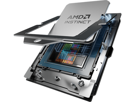
As the world rapidly embraces artificial intelligence, the demand for powerful GPU solutions has skyrocketed. In this evolving landscape, the AMD Instinct MI300X emerges as a revolutionary force, setting a new benchmark in AI Acceleration, performance, and memory capacity. When paired with SharonAI’s state-of-the-art Cloud Computing infrastructure, this powerhouse transforms how enterprises handle deep learning, HPC, and generative AI workloads.
At the heart of the MI300X’s excellence is its advanced CDNA 3 architecture. With an enormous 192 GB of HBM3 memory and up to 5.3 TB/s of memory bandwidth, it delivers the kind of GPUpower that modern AI and machine learning workloads demand. From training massive language models to running simulations at scale, the AMD Instinct MI300X ensures speed and efficiency without compromise. For organizations pushing the boundaries of infrastructure, this level of performance offers unprecedented flexibility and scale.
SharonAI, a leader in GPU cloud solutions, has integrated the AMD Instinct MI300X into its global infrastructure, offering clients access to one of the most powerful AIGPU solutions available. Whether you're a startup building new GenerativeAI models or an enterprise running critical HPC applications, SharonAI’s MI300X-powered virtual machines deliver high-throughput, low-latency computing environments optimized for today’s AI needs.
One of the standout advantages of the MI300X lies in its ability to hold massive models in memory without needing to split them across devices. This is particularly beneficial for Deep Learning applications that require processing large datasets and models with billions—or even trillions—of parameters. With MI300X on SharonAI’s cloud, developers and data scientists can now train and deploy these models faster, more efficiently, and more cost-effectively than ever before.
Another key strength of this collaboration is its open-source flexibility. Powered by AMD’s ROCm software stack, the MI300X supports popular AI frameworks like PyTorch, TensorFlow, and JAX. This makes integration seamless and ensures that teams can continue building without major workflow changes. For those who prioritize vendor-neutral infrastructure and future-ready systems, this combination of hardware and software offers the ideal solution.
SharonAI has further distinguished itself with a strong commitment to sustainability and scalability. Its high-performance data centers are designed to support dense GPU workloads while maintaining carbon efficiency—a major win for enterprises that value green technology alongside cutting-edge performance.In summary, the synergy between AMD Instinct MI300X and SharonAI provides a compelling solution for businesses looking to accelerate their AI journey. From groundbreaking GenerativeAI to mission-critical HPC, this combination delivers the GPUpower, scalability, and flexibility needed to thrive in the AI era. For any organization looking to enhance its ML infrastructure through powerful, cloud-based AIGPU solutions, SharonAI’s MI300X offerings represent the future of AI Acceleration and Cloud Computing.
#AMDInstinctMI300X#AIAcceleration#DeepLearning#GenerativeAI#HPC#MLInfrastructure#CloudComputing#DataScience#AIResearch#SharonAI
0 notes
Text
0 notes
Text
0 notes
Text
0 notes
Photo

🔍 What's next for Samsung?! The tech giant is sampling its cutting-edge HBM4 memory to tech leaders like NVIDIA, Google, and Broadcom. Despite previous hurdles with its HBM3, Samsung's hopeful for a turnaround. The HBM market is expected to surge by 10% by 2025, emphasizing the increasing demand for advanced memory technology. Samsung utilizes some of its best technology, including its 4nm process, aiming to meet competitors' standards. The question remains: Will companies trust Samsung's HBM solutions with fierce competition from SK hynix and Micron? Are you excited about the future of memory technology? How do you think Samsung will fare in this high-stakes race? Share your thoughts below! 🚀 #Samsung #HBM4 #TechNews #NVIDIA #Broadcom #Google #MemoryTechnology #Innovation #TechIndustry #Competition #TechTrends
0 notes
Quote
2024年12月03日 11時45分 アメリカが中国のAI軍事利用を懸念して広帯域幅メモリ(HBM)の輸出規制を強化し中国企業140社をエンティティリストに追加 アメリカ商務省の産業安全保障局(BIS)が、中国に対する広帯域幅メモリ(HBM)の輸出規制強化を発表しました。合わせて、半導体企業や投資企業を含む140におよぶ中国の事業体がエンティティリスト(取引規制対象リスト)へ追加されています。 Commerce Strengthens Export Controls to Restrict China’s Capability to Produce Advanced Semiconductors for Military Applications | Bureau of Industry and Security https://www.bis.gov/press-release/commerce-strengthens-export-controls-restrict-chinas-capability-produce-advanced BISは「中国の最高指導部はICチップを国家安全保障および軍事力にとって重要なものとみなしており、中国独自の自給自足の半導体エコシステムの構築を重要課題に設定している。中国共産党の半導体戦略は軍事力の近代化や、大量破壊兵器の開発、人権抑圧の推進を意図しており、アメリカと同盟国の安全保障を脅かしている」と述べ、中国による半導体開発能力の抑制を目的として規制を強化することを発表しました。 BISは「戦争の未来を変えてしまう可能性のある中国のAI研究を遅延させる」「中国独自の半導体エコシステムの構築を阻害する」の2点を焦点に、「半導体製造装置」「半導体製造ソフトウェア」「HBM」の輸出に関する規制強化を実施しました。 AIの研究開発には高性能な計算処理チップのほかに、大量のデータを高速に転送できるHBMも重要です。BISはアメリカ製のHBMだけでなく、外国産のHBMも規制の対象に加えており、中国国内で高性能なHBMが入手困難となる可能性があります。なお、先進的なHBMの開発企業としては、アメリカ企業のMicronのほかに韓国企業のSK hynixやSamsungが有名です。 Samsungの第4世代高帯域幅メモリの「HBM3」チップがNVIDIAのテストに合格、中国市場向けの「H20」に搭載���定 - GIGAZINE また、BISは自国の安全保障にリスクを与える事業体や大量破壊兵器を拡散させるリスクのある事業体を「エンティティリスト」に登録し、登録事業体に対する輸出を規制しています。新たに、140におよぶ中国の事業体をエンティティリストへ追加し、14件の修正を加えたことが明らかになりました。追加された事業体には「中国政府の要請に従って高性能半導体の生産のために活動している半導体工場、ツール開発企業、投資企業」が含まれています。 規制強化の発表に際して、ジーナ・レモンド商務長官は「今回の規制強化は、バイデン=ハリス政権が同盟国およびパートナー国と協力して定めた『中国の先進技術生産能力の阻害』という目標の集大成である。アメリカの輸出管理のさらなる強化は、商務省がアメリカの国家安全保障戦略の中心的役割を担っていることを示している。輸出管理を通じて中国の軍事近代化に戦略的に対処するうえで、バイデン=ハリス政権ほど強固な政権はない」とコメントしています。 なお、BISが発行しているエンティティリストは、以下のリンク先で確認できます。 eCFR :: Supplement No. 4 to Part 744, Title 15 -- Entity List https://www.ecfr.gov/current/title-15/subtitle-B/chapter-VII/subchapter-C/part-744/appendix-Supplement No. 4 to Part 744 この記事のタイトルとURLをコピーする ・関連記事 ジョー・バイデンと習近平が「核兵器を管理するのはAIではなく人間であるべき」という考えに同意 - GIGAZINE 中国のチップ自給率は2014年の約14%から2023年には23%に上昇、2027年には27%に達すると予想されている - GIGAZINE 中国のAI企業DeepSeekがOpenAI o1に匹敵する推論AIモデル「DeepSeek-R1-Lite-Preview」公開、オープンソース化する計画も - GIGAZINE 中国による2025年~2027年の半導体製造設備投資は14兆円超えになるとの予測、韓国と台湾は10兆円超えでアメリカは9兆円規模か - GIGAZINE 中国政府が国内のAI企業に「NVIDIA製チップをボイコットせよ」と指示、アメリカの制裁に対抗するため - GIGAZINE 日本政府がチップ・量子コンピューティング・AI産業の強化を目的に約1兆5000億円の補正予算を割り当て、一部はチップ新興企業Rapidusへ - GIGAZINE ・関連コンテンツ 中国政府が第14次五カ年計画で国内のチップ産業を全面支援しアメリカの規制に対抗 量子コンピューティングや半導体製品を含む重要技術に関する新たな輸出規制案をアメリカ政府が発表、日本・オランダ・その他の同盟国と調整中 バイデン政権が国家の安全を脅かす可能性のある中国のAI技術等の取引・投資を制限する規則を策定、2025年1月から施行 NVIDIAやAMDに対し「中国へのAIチップの輸出規制」をアメリカ政府が命じる アメリカによるHuaweiおよび関連企業への輸出管理がさらに強化、新たに38の関連企業をリストに追加 半導体大手・Micronの製品が「安全審査を通らなかった」として中国がインフラ管理者に購入禁止を呼びかけ 「中国がAIとスパコンを駆使して兵器開発や暗号解読を行うのではないか」という疑念でアメリカは中国への半導体輸出を取り締まっている アメリカが中国へのAIチップ輸出制限を強化しNVIDIA製チップの輸出が困難に
アメリカが中国のAI軍事利用を懸念して広帯域幅メモリ(HBM)の輸出規制を強化し中国企業140社をエンティティリストに追加 - GIGAZINE
0 notes
Text
Exploring HBM3e Features: What’s New and Noteworthy

The creation of the world’s fastest HBM3e DRAM has been verified by SK hynix, and samples are now being sent to NVIDIA and other clients for testing purposes.
The HBM3e DRAM from SK Hynix is not only faster, but it also provides higher capacities, improved heat dissipation, and easy compatibility.
It was reported in June that NVIDIA had made a request to SK hynix to sample their next-generation HBM3e DRAM. This request became a reality when NVIDIA introduced its GH200 GPU with enhanced HBM3e DRAM, giving up to 5 TB/s bandwidth per chip. SK hynix was able to fulfill this request.
SK Hynix Inc. has issued the following press release to indicate that it has successfully created HBM3E, the next-generation of the highest-specification DRAM for AI applications that is presently available, and that a customer’s examination of samples is now under way.
On top of its expertise as the industry’s single mass supplier of HBM3, the business claimed that the successful creation of HBM3E, the extended version of HBM3 which offers the world’s finest specifications, comes on top of its experience as the extended version of HBM3. With its expertise as the supplier of the industry’s biggest volume of HBM products and the mass-production readiness level, SK hynix wants to mass-produce HBM3E in the first half of next year and strengthen its unparalleled leadership in the AI memory market. This will be accomplished by using its experience as the supplier of the industry’s largest volume of HBM goods.
The business claims that its most recent product not only satisfies the industry’s most stringent criteria for speed, which is the most important need for artificial intelligence memory devices, but also excels in all other areas, such as capacity, heat dissipation, and user-friendliness.
In terms of processing speed, the HBM3E is capable of handling data at a rate of up to 1.15 terabytes (TB) per second. This is the same as being able to process more than 230 Full-HD movies that are each 5GB in size in a single second.
The cutting-edge technology of the Advanced Mass Reflow Molded Underfill, also known as MR-MUF**, has been integrated onto the most recent version of the product, which has resulted in a 10% increase in the rate at which heat is dissipated. In addition to this, it offers backward compatibility, which makes it possible to implement the most recent product onto systems that have already been designed for HBM3 without having to make any modifications to their structures or designs.
MR-MUF: a process of attaching chips to circuits and filling the space between chips with a liquid material when stacking chips instead of laying a film to improve efficiency and heat dissipation
Backward Compatibility: an ability to allow interoperability between an older and a new system without modification to the design, especially in information technology and computing spaces. A new memory product with backward compatibility allows continued use of the existing CPUs and GPUs without modifications to design
“We have a long history of working with SK hynix on High Bandwidth Memory for leading-edge accelerated computing solutions,” said Ian Buck, Vice President of Hyperscale and HPC Computing at NVIDIA. “We look forward to continuing our collaboration with HBM3E to deliver the next generation of AI computing.”
According to Sungsoo Ryu, who serves as the Head of DRAM Product Planning at SK hynix, the business has enhanced its market leadership via the creation of HBM3E. This was accomplished by further expanding the completeness of the HBM product range, which is in the limelight as a result of the growth of AI technology. “SK hynix will also work toward achieving a rapid turnaround in its business by increasing the supply share of the high-value HBM products,”
0 notes
Text
NVIDIA H200 vs H100: Which GPU Reigns Supreme in the AI Cloud?
The rapid evolution of artificial intelligence (AI) has necessitated advancements in hardware, particularly in graphics processing units (GPUs). NVIDIA's H100 and H200 GPUs are at the forefront of this evolution, designed specifically for high-performance computing (HPC) and AI workloads. This blog delves into a comprehensive comparison of the NVIDIA H200 vs H100, exploring their specifications, performance metrics, benefits, challenges, and real-world applications across various industries.
Overview of NVIDIA H100 and H200
NVIDIA's Hopper architecture underpins both the H100 and H200 GPUs, but the H200 represents a significant leap forward in terms of capabilities.
NVIDIA H100: Launched as a robust option for AI and HPC tasks, it features:
Memory: 80 GB of HBM3 memory
Bandwidth: Approximately 3.35 TB/s
Performance: Strong throughput for generative AI and traditional HPC applications
NVIDIA H200: The latest entrant in the lineup, it boasts:
Memory: 141 GB of next-gen HBM3e memory
Bandwidth: 4.8 TB/s, representing a 1.4x increase over the H100
Performance: Up to 2x faster inference for large language models (LLMs) compared to the H100
Statistical Insights and Performance Benchmarks
The performance improvements from the H100 to the H200 are substantial:
Training Speed: The H200 can reduce training time by up to 45% for large models like Llama-3.1 (405B), thanks to its enhanced memory bandwidth and capacity.
Inference Performance: The H200 achieves nearly double the inference speed on models like Llama 2-70B compared to the H100. This is crucial for applications requiring real-time data processing.
Total Cost of Ownership (TCO): The energy efficiency of the H200 is noteworthy; it is estimated to consume up to 50% less energy than the H100 during inference tasks, leading to a significantly lower TCO over its lifespan.
Benefits of Upgrading to NVIDIA H200
Increased Memory Capacity: With 141 GB of memory, the H200 can handle larger datasets and more complex models without bottlenecks.
Higher Bandwidth: The improved bandwidth allows for faster data transfer rates, essential for training large-scale AI models efficiently.
Cost Efficiency: Lower energy consumption translates to reduced operational costs, making it an attractive option for enterprises focusing on long-term investments in AI cloud infrastructure.
Enhanced Scalability: The ability to scale across multi-GPU clusters with better interconnectivity (900GB/s NVLink) ensures that organizations can expand their capabilities as their needs grow.
Current Challenges Facing NVIDIA GPUs
Despite their advantages, several challenges persist:
Cost Considerations: The initial investment for the H200 is significantly higher than that of the H100, which may deter smaller organizations or startups from upgrading.
Software Optimization: While hardware improvements are substantial, software ecosystems must also evolve to fully leverage these advancements. Ensuring compatibility with existing frameworks can be a hurdle.
Supply Chain Issues: As demand for GPUs surges, supply chain constraints may affect availability and lead times for acquiring these advanced units.
Industries Benefiting from NVIDIA GPUs
The advancements in GPU technology have far-reaching implications across various sectors:
Healthcare: Accelerated drug discovery processes through complex simulations and AI-driven diagnostics.
Finance: Real-time fraud detection systems leveraging LLMs for transaction analysis.
Automotive: Enhanced capabilities in autonomous driving systems through improved data processing speeds.
Entertainment: Faster rendering times for graphics-intensive applications such as video games and CGI in films.
Use Cases and Case Studies
Healthcare AI Models: A leading pharmaceutical company implemented the H200 to expedite drug discovery processes. By utilizing its memory capacity and bandwidth, they reduced simulation times by over 50%, allowing faster iterations on drug candidates.
Financial Services Optimization: A major bank adopted the H200 for fraud detection algorithms, resulting in a significant reduction in false positives while increasing detection rates by nearly 30%. This was achieved through enhanced model training capabilities.
Autonomous Vehicle Development: An automotive manufacturer leveraged the superior inference speed of the H200 to improve real-time decision-making processes in autonomous vehicles. This resulted in safer navigation systems capable of processing vast amounts of sensor data instantaneously.
Conclusion
In conclusion, while both the NVIDIA H100 and H200 GPUs are formidable options for AI workloads within cloud environments, the advancements seen in the H200 make it a superior choice for organizations looking to push boundaries in AI development. With its enhanced memory capacity, increased bandwidth, and improved energy efficiency, the H200 stands out as a game-changer in high-performance computing.
Organizations must weigh their specific needs against budgetary constraints when deciding between these two powerful GPUs. However, as industries increasingly rely on sophisticated AI applications, investing in cutting-edge technology like the NVIDIA H200 could provide significant competitive advantages moving forward.
By understanding these differences and potential applications, businesses can make informed decisions that align with their strategic goals in an ever-evolving digital landscape.
0 notes
Link
#3Dstacking#co-optimization#HBMadvancement#manufacturingscaling#memoryarchitecture#regionalspecialization#semiconductorinnovation#supplychainresilience
0 notes
Text
NVIDIA H100 Tensor Core GPU Explained: Features, Performance & Use Cases
Introducing the NVIDIA H100 Tensor Core GPU: Powered by Hopper Architecture
At the heart of the NVIDIA H100 Tensor Core GPU is the revolutionary Hopper™ architecture. Featuring the groundbreaking Transformer Engine and fourth-generation Tensor Cores, this GPU is built specifically to accelerate AI workloads at unprecedented speeds. It’s a powerful leap forward for training massive deep learning models and running complex simulations.
Advanced Memory and Lightning-Fast Compute Capabilities
The NVIDIA H100 Tensor Core GPU offers unmatched memory configurations:
80GB HBM3 memory (SXM version)
94GB HBM3 memory (NVL version)
With an astonishing 3,958 TFLOPS FP8 performance, the H100 provides up to 4x faster AI training compared to previous models. This level of computational power ensures quicker insights, faster model deployment, and accelerated scientific discovery.
0 notes