#reflow oven
Text
Reflow Oven | Gtsmt.com

Experience precise reflow soldering with GT SMT's reflow ovens. Our state-of-the-art equipment ensures optimal temperature profiles for consistent results. Discover our range of reflow ovens at GT SMT for efficient PCB assembly.
Reflow Oven
0 notes
Text


reflow oven i built, worked great till i threw it out.. smooth move! 🙄
1 note
·
View note
Text
Reflow solder oven

REFLOW SOLDER OVEN SERIES
The cooling is more rapid than the heating, as fast cooling encourages the solder to form into a crystalline structure which creates a superior bond to the underlying board. The fourth chamber quickly cools the board, down to temperatures of 86 Degrees Fahrenheit. This process generally takes 30-40 seconds. Timing is crucial here, as the solder must melt fully without having time to flow off the board or start vaporizing. Several heating methods can be used here, although conventional convection baking is still the most common. The heart of the reflow soldering process happens here, where the circuit board is rapidly heated to maximum temperatures to fully melt the solder and bond it to the circuit board. Once the thermal soak is finished and the piece moves on, the board should be at thermal equilibrium. This ensures even heat distribution, as well as activating chemicals in the solder paste that prevent the solder from turning into microbeads, which it otherwise would. Having reached the desired pre-heating point, the board passes to the second chamber for a thermal soak at that temperature, for 60-120 seconds. This stage can last several minutes, as the temperature is only raised by about 3-5 degrees Fahrenheit per second. The heat distribution must be uniform, or the board could warp. The first and lengthiest stage is the pre-heating of the circuit, which requires bringing it up to a given temperature slowly.
REFLOW SOLDER OVEN SERIES
These marvels of engineering can automatically handle the heating and cooling of each circuit board, sending it through a series of internal chambers for treatment. Modern manufacturers utilizing surface mounted technology use all-in-one devices called Reflow Soldering Ovens to ensure proper circuit boards. Much like when cooking dinner, too little or too much heat can quickly ruin the project. While there are several possible techniques, the board has to be precisely raised to temperatures in excess of 200 degrees, to properly melt the solder. The hard part is the baking that follows. Rather than using space-hungry holes through the board, SMT-based circuits have components which are placed directly onto the board, using a solder paste which also works as a glue. Manufacturing based on Surface-Mounted Technology has taken over electrical engineering, and for good reason.
1 note
·
View note
Text
Pcb reflow oven

PCB REFLOW OVEN PRO
PCB REFLOW OVEN SOFTWARE
PCB REFLOW OVEN PROFESSIONAL
PCB REFLOW OVEN SIMULATOR
aerospace, military, telecommunications) reflow soldering in a Nitrogen gas atmosphere with low levels of Oxygen is common and is a preferred setup. However, for mission critical or high reliability applications (i.e. Most PCBs are reflowed in an air atmosphere with great results.
PCB REFLOW OVEN PRO
Increased productivity, superior performance and ease of operation make the PRO 1600 a versatile system ideal for small to medium run production, prototyping, NPI, testing or curing. An optional Video Recording and Observation Module allows taking high magnification images and recording video during a soldering cycle. With the optional External Thermocouple Control ( ETC), profiles may be processed based on temperature readings of the assembly, not the air temperature around it. Even for prototypes, this often means avoiding to spend hours of testing and debugging failed boards. Maintaining a low delta T across all of the components on the assembly ensures that they are not overheated or thermally stressed.
PCB REFLOW OVEN SOFTWARE
Precise software control delivers unsurpassed temperature uniformity. Where other batch and conveyor ovens fail to meet the desired profile curve, PRO 1600 excels. It offers a unique On-The-Fly settings adjustment capability that allows creating and optimizing profiles all in a single pass. Sealed heating chamber enables ramp up rates of up to 4° Celsius/second from ambient and programming of up to 10 profile zones. PRO 1600 is very user friendly in terms of profile creation and modification. It has been designed for reflow soldering of even the most challenging applications including metal core, high thermal mass, RF / microwave housings, wafer boards, and ceramic assemblies. PRO 1600 is a forced air / nitrogen convection reflow oven with a small footprint measuring only 31″ x 31″ (80cm x 80cm). We are happy to discuss your soldering oven requirements in detail, and will gladly come up with realistic solutions for your team so you can begin soldering circuit boards with detailed precision today! If you would like to get in touch with our expert soldering circuit board and soldering oven team, give us a call for more information.
PCB REFLOW OVEN SIMULATOR
Compatible with a variety of custom coupons and requiring minimal operator involvement, our reflow simulator provides ultra-accurate data reports and assembly analysis with simplicity. With PCB soldering machines and SMT reflow ovens designed to last, our superlative products are the perfect addition to your business for all of your soldering furnace needs.īeyond the extensive soldering circuit board and soldering oven solutions we provide, we also produce a reflow simulator for advanced microvia and IPC D coupon testing.
PCB REFLOW OVEN PROFESSIONAL
Our professional technicians offer complete reflow soldering machines and prototype reflow oven installation, calibration, and guidance. With on-the-fly profile adjustment and ultra-accurate temperature control at the circuit assembly, our reflow oven is expediting process development and improves yields. Thanks to our advanced software integration, with powerful heating capability, our SMT reflow oven achieves the user-friendly end goal. Our team wanted to create an SMT oven catering to the end user with a simplified setup and ease of operation. Our reflow ovens aim to bridge the gap between low end ovens and large scale production machines with consistent heating profiles, a simple user interface, process automation, and detailed data for complete transparency and consistency throughout the SMT ( Surface Mount Technology) reflow process. The focus is to achieve guaranteed high quality product with strong and reliable solder joints. This includes precise temperature monitoring at the circuit assembly and if necessary ability to purge Nitrogen within the reflow chamber for Oxygen concentration down to 10 PPM. While many reflow ovens on the market are adequate for simple soldering projects, we designed the PRO 1600 to be a high end oven with capabilities matching large scale production ovens. Our engineers developed the PRO 1600 SMT Reflow Oven to solve a variety of common issues associated with inconsistent reflow soldering in batch and benchtop tunnel ovens. Dedicated to quality engineering and superior service, our soldering machines and reflow ovens achieve repeatable, high quality results customers can count on. As a leading batch soldering machine and solder reflow manufacturer, we are on a mission to provide innovative solutions for the ever-evolving demands within the printed circuit board industry. With nearly 40 years of experience in developing and manufacturing circuit board soldering equipment, ATCO is now offering the second generation PRO 1600 SMT Reflow Oven.
0 notes
Text
Reflow ovens

There will be an 8.32 cm spacing between the boards in the oven. To summarize: for our 45 cm board that has a cycle time of 40 seconds, we need a 10-zone oven with a heated tunnel length of 360 cm. These machines vary in size from small boxy. Let’s calculate what it will be:īS = (BL + Spacing)/CT = 1.33 cm/sec => BL+ Spacing = BS x CT => Spacing = BS x CT – BL A SMT reflow oven is an essential machine of the thermal processing of solder for electronics manufacturing. The extra belt speed will allow for a small amount of spacing between the boards. Success! Since 1.33 cm/sec is greater than 1.1125 cm/sec, this 10-zone oven will work. How about the 10-zone oven? Let’s see if the belt speed is greater than the 1.125 cm/sec needed.īS = HTL/Time = 360 cm/270 seconds 1.33 cm/sec Now we can see that the 7-zone oven won’t do the job either. What about a 7-zone oven? Let’s calculate the belt speed for this oven.īS = HTL/Time = 250 cm/270 seconds 0.926 cm/sec The component placers will be presenting a 45 cm board every 40 seconds, so the belt speed needs to be:īS = Board Length/Cycle Time = BL/CT = 45 cm/40 sec = 1.125 cm/sec So if we choose the 5 zone oven the belt speed will be:īelt Speed = BS= Heat Tunnel Length/Time in Heated Tunnel = HTL/Time = 180 cm/270 seconds 0.66 cm/sec SMT Reflow ovens accept PCBs with mounted components in wet solder paste and produce soldered PCBs using convection heating to reflow the solder paste. By studying the reflow profile in above, we see that the amount of time needed in the heated zone is about 4.5 minutes or 270 seconds. Let’s assume that you will be using a typical modern SAC solder paste. Table 1 shows some typical reflow oven metrics: Let’s make some calculations and see if your concerns are justified. But, you are concerned that a 5-zone oven may not have the capacity that is needed to keep up with the component placement machines. Your boss is pressuring you to get another 5-zone oven, as they are cheaper and take up much less space than a 7- or 10-zone oven. The boards are 45 cm long and you expect the cycle time from the component placement machines to be 40 seconds per board. You are putting in a new assembly line to assemble some large boards for which your company just received a 3-year contract. SiP & Heterogeneous Integration & Assembly (HIA).The Indium Corporation & Macartney Family Foundation.Learn more about our products, their applications, find a distributor or access online resources. Our products meet strict regulatory requirements and many are are sustainable, helping protect both people and the planet. MicroCare and its sub-brands, MicroCare Medical, Sticklers and Stereze formulate and blend cleaning coating, lubricating and sterilization fluids used in the manufacture, installation and use of products in the electronics, medical device manufacturing, fiber optic, metal finishing, industrial maintenance and healthcare infection prevention industries. Use with MicroCare lint-free cleaning wipes (MCC-W11) for best results. The noncorrosive fluid is ESD-safe and is safe to use on all metals, synthetics, plastics and elastomers. Money-saving, refillable pump-spray bottle is not TriggerGrip™ compatible. Suitable for use in hand wipe applications or ultrasonic tanks, this cleaner reduces equipment down-time and lowers cleaning costs.Ĭonvenient Packaging Options: The popular 'cubitainers' are easy to store on a shelf and feature a faucet-like valve so the fluid can be dispensed without lifting the container. So, cleaning actually becomes easier over time. During the soldering process, evaporated fluxes as well as gas emissions from solder resist are deposited onto the internal surfaces of. Plus, Reflow Oven Cleaner avoids one of the big problems of alcohol cleaners - the curing and hardening of flux residues in the oven. While I can solder most SMD components by hand, and most components can be bought on break-out boards, I decided that it was time to up my game in the SMD soldering department. This product is so much stronger than IPA alcohol that it slashes oven cleaning times 50% or more while improving cleaning results. Recently, many of my electronics projects have required the use of components that are only available in SMD form. Made with water, alkaloids and proprietary long-chain alcoholsīecause this reflow oven cleaner is nonflammable you can clean the oven while it is still warm, saving time and enhancing the cleaning because warm solvents clean better than cold ones.Cleans all solder paste and flux residues, including RMA, no-clean and lead-free products.Four times faster than IPA (isopropyl alcohol).Activated by the residual heat of the oven.Speeds cleaning of ovens even when warm.Cleaning reflow ovens - in this case, a Heller unit - can be a challenge because of the flux residues that coat the inside of the machines Features:
0 notes
Text
Selective soldering 🔧🔬🔥
Selective soldering involves attaching specific components to printed circuit boards (PCBs) and molded modules, a method particularly useful for items susceptible to heat damage from standard reflow ovens or wave soldering found in conventional surface-mount technology (SMT) or through-hole assembly techniques. Typically, this method is applied after an initial SMT oven reflow phase. The components targeted for selective soldering are often nestled among others already soldered via a surface-mount reflow method. This demands high precision in the selective soldering process to prevent damage to the surrounding elements.
#adafruit#selectivesoldering#pcbassembly#electronicsmanufacturing#surface-mount#throughhole#reflowprocess#precisionengineering#solderingtechnology#circuitboarddesign#manufacturinginnovation#techadvancements
5 notes
·
View notes
Text
What is PCB Assembly ?
PCB Assembly manufacturer - Hitech Circuits Co., Limited
It’s the step in the manufacturing process in which you populate a blank board with the electronic components needed to make it into a functional printed circuit board. It’s these components that make a board into the circuit that enables an electronic product to function. PCB assembly typically takes place via one of two processes:
1. Surface-mount technology
SMT: SMT stands for “Surface Mount Technology“. The SMT components are very small sizes and comes in various packages like 0201, 0402, 0603, 1608 packages for resistors and capacitors. Similarly for Integrated circuits ICs we have SOIC, TSSOP, QFP and BGA.
The SMT components assembly is very difficult for human hands and can be time taking process so it is mostly done by automated pick and place machine.
2. Through-hole manufacturing
THT: THT stands for “Through hole Technology”. The components with leads and wires, like resistors, capacitors, inductors, PDIP ICs, transformers, transistors, IGBTs, MOSFETS are example.
The component has to be inserted on one side of PCB and pulled by leg on other side and cut the leg and solder it. The THT components assembly is usually done by hand soldering and is relatively easy.
Printed Circuit Board Assembly Techniques
There are only two common PCBA techniques available for use by a PCB designer. The methods are:
1. Automated PCB Assembly Techniques
Generally, this technique employs the use of state of the art machines, which are fully automatic. For example, the surface mount components are worth positioning with the aid of an automated pick and place machine.
Again, reflow soldering is commonly for surface mount components usually done in a reflow oven. An automated solder stencil is also used to apply the solder paste on the PCB.
Finally, high tech inspection machines are used to confirm and check the quality of the PCBA. Some of which include: Automated optical inspection machine (AOI), X-ray inspection machines, etc.
Above all, due to the precise monitoring, control of soldering, no human input and versatile machines.
This technique ensures utmost efficiency, output consistencies, and limits defects.
2. Manual PCB Assembly Techniques
This method is favorite for use with through-hole parts, which needs manual placement on the board. Besides, with these through-hole parts, it’s advisable you use wave soldering. Note that in the through- hole assembly process, you need to place the components and electronics on the PCB.
After that, you use wave soldering to solder the leads. Typically, you will need an individual to insert a component into a marked PTH. Once done, transfer the PCB to the next station where the next person will be on standby tasked with fixing another part.
What are the Benefits of SMT PCB Assembly?
SMT assembly provides many benefits and some of them are as follows:
It can be used to incorporate small components.
In SMT, the components can be placed on both sides of the board.
It assures high component densities.
Fewer holes need to be drilled for surface mounting than through-hole.
It require low initial costs and time for setting up the mass production.
SMT is the simpler and faster-automated assembly when compared to through-hole.
Errors regarding the component placement can be easily rectified.
Surface mount PCBs feature strong joints, which can easily withstand vibrations.
What are the techniques used in Surface Mount Technology?
There are several techniques for the reflow process. After applying the solder paste or a flux mixture on the board and after placing the components, the boards are conveyed to a reflow soldering oven. The techniques used for reflowing soldering include infrared lamps, hot gas convection, fluorocarbon liquids with a high boiling point, and so on.
What are the different testing methods used in SMT PCB Assembly?
Hitech Circuits as the PCB assembly manufacturer, we perform the following testing and inspection to ensure the quality of surface mount PCBs.
Automated Optical Inspection (AOI): This is performed before and after the soldering to identify the component placement, presence, and solder quality.
X-ray Testing: In this type of testing, the operator relies on the X-ray images of the PCB to check the solder joints and lead-less components such as Quad Flat Packs and ball grid arrays, which are generally not visible to naked eyes.
In-Circuit Testing (ICT): This method is used to detect manufacturing defects by testing the electrical properties in the SMT Assembly.
What type of files or documents should I send for SMT PCB Assembly?
Gerber Files: The file contains all details of physical board layers including solder masks, copper layers, drill data, legends, and so on.
Bill of Materials (BOM): This contains information on the list of items needed for the PCB manufacturing and the instructions of manufacturing.
Pick and Place File: This file contains information on all components to be used in the PCB design and their rotation and X-Y coordinates.
The whole process of PCB Assembly
1. Bare board loader machine
The first step in the PCB assembly is to arrange the bare boards on the rack, and the machine will automatically send the boards one by one into the SMT assembly line.
2. Printing solder paste
When PCB on the SMT production line, firstly, we have to print solder paste on it, and the solder paste will be printed on the pads of the PCB. These solder pastes will be melt and solder the electronic parts to the circuit board when it passes through the high-temperature reflow oven.
In addition, when testing new products, some people will use film board/adhesive cardboard instead of solder paste, which can increase the efficiency for adjusting the SMT machines.
3. Solder paste inspection machine(SPI)
Since the quality of solder paste printing is related to the quality of welding of subsequent parts, some SMT factories will use optical machine to check the quality of solder paste after printed the solder paste in order to ensure stable quality. If there any poorly printed solder paste board, we will wash off the solder paste on it and reprint, or remove the excess solder paste if there is redundant solder paste on it.
4. High speed SMT machine
Usually, we will put some small electronic parts (such as small resistors, capacitors, and inductors) to be printed on the circuit board first, and these parts will be slightly stuck by the solder paste just printed on the circuit board, so even if the speed of printing is very fast and the parts on the board will not fall away. But large parts are not suitable for use in such high speed SMT machines, which will slow down the speed of small parts assembly. And the parts will be shifted from the original position due to the rapid movement of the board.
5. Universal SMT machine
Universal SMT machine is also known as "slow machine", it will be assembled some large electronic components, such as BGA IC, connectors, etc., these parts need more accurate positions, so the alignment is very important. Use a camera to take a picture to confirm the position of the parts, so the speed is much slower than High speed SMT machine we taked before. Due to the size of the components here, not all of them are packed in tape and reel, and some may be packed in trays or tubes. But if you want the SMT machine to recognize the trays or tube-shaped packaging materials, you must configure an additional machine.
Generally, traditional SMT machines are using the principle of suction to move electronic parts, and in order to place the parts successfully, and there must be the flat surface on these electronic components for the suction nozzle of the SMT machine to absorb. However, for some electronic parts don’t have a flat surface for these machines, and it is necessary to order special nozzles for these special-shaped parts, or add a flat tape on the parts, or wear a flat cap for thees electronic parts.
6. Manual parts or visual inspection
After assembled all parts by the high speed SMT machine or Universal SMT machine and before going through the high-temperature reflow oven, and we will set up a visual inspection station here and to pick out the deviation parts or missing components boards etc., because we have to use a soldering iron to repair if there are still defectives boards after passing the high-temperature oven, which will affect the quality of the product and will also increase the cost. in addition, for some larger electronic parts or traditional DIP parts or some special reasons cannot be processed by the SMT machine before, they will be manually placed on pcb here.
7. Reflow oven
The purpose of reflow oven is to melt the solder paste and form a non-metallic compound on the component feet and the circuit board, that means to solder electronic components on the circuit board. The temperature rise and fall curves often affect the soldering quality of the entire circuit board. According to the characteristics of the solder materials, usually the reflow oven will set the preheating zone, soaking zone, reflow zone, and cooling zone to achieve the best soldering effect.
For example, the melting point for SAC305 solder paste with lead-free is about 217°C, which means that the temperature of the reflow oven must be higher than the melting points to remelt the solder paste. What's more, the maximum temperature in the reflow furnace should not exceed 250°C, otherwise many parts will be deformed or melted because they cannot withstand such a high temperature.
Basically, after the pcb passed through the reflow oven, the assembly for the entire circuit board is almost complete. If there are hand-soldered parts, we need to transfer to DIP process, and then we have to check the quality after reflow oven by QC department.
8. Automatic optical inspection(AOI)
The main purpose of setting up AOI is because some high density boards can’t be process the following ICT test, so we used AOI inspection to replace it. But even using AOI inspections, there still have the blind spots for such checking, for example, the solder pads under the components cannot be checked by AOI. At present, it can only check whether the parts have side standing issue, missing parts, displacement, polarity direction, solder bridges, lack of soldering etc., but cannot checking the BGA solderability, resistance value, capacitance value, inductance value and other components quality, so far AOI inspection can’t completely replace ICT test.
Therefore, there is still some risk if only AOI inspection is used to replace ICT testing, but ICT test is also not 100% make sure the good quality, we suggest these two ways can be combined with together to make sure the good quality.
9. PCB unloader machine
After the board is fully assembled, it will be retracted to the unloder machine, which has been designed to allow the SMT machine to automatically pick and place the board without damaging the quality for PCB.
10. Visual inspection for finished products
Normally there will be a visual inspection area in our SMT production line whether there is an AOI station or not, and it will help to check if there are any defectives after completed assembled the pcbs. If there is an AOI station, it can reduce the visual inspection worker on our SMT line, and to reduce the potential cost, and because it is still necessary to check some places that cannot be judged by AOI, many SMT factories will provide the mainly visual inspection templates at this station, which is convenient for visual inspection worker to inspect some key parts and polarity for components.
11. DIP process
DIP process is a very important process in the whole PCBA processing, and the processing quality will directly affect the functional for PCBA boards, so it is necessary to pay more attention to the DIP process. There are many preliminary preparations for DIP process. The basic process is to re-process the electronic components first, like to cut the extra pins for some DIP components, our staff received the components according to the BOM list, and will check whether the material part numbers and specifications are correct or not, and performs pre-production pre-processing according to the PCBA samples. The steps are: Use various related equipment (automatic capacitor pins cutting machine, jumper bending machine, diode and triode automatic forming machine, automatic belt forming machine and other machines) for processing.

12. ICT test
Printed Circuit board open/short circuit test (ICT, In-Circuit Test), The purpose of ICT test is mainly to test whether the components and circuits on the printed circuit board are open or short issues. It can also measure the basic characteristics of most components, such as resistance, capacitance, and inductance values to judge whether the functions of these parts are damaged, wrong parts or missing parts etc. after passing through the high-temperature reflow oven.
ICT test machines are divided into advanced and basic machines. The basic ICT test machines are generally called MDA (Manufacturing Defect Analyzer). It’s just to measure the basic characteristics of electronic components and judge open and short circuits issue we talked above.
In addition to all the functions of the basic ICT test machines, for advanced ICT test machine can also test the whole PCBA by using power, start to testing the PCBA boards by setting the program in the test machine. The advantage is that it can simulate the function of the printed circuit board under the actual power-on condition, this test can partly replace the following functional test machine (Function Test). But the cost for the test fixture of this advanced ICT test can probably buy a car, it’s too expensive and we suggest it can be used in mass production products.
13. PCBA function test
Functional testing is to make up for the ICT test, because ICT only tests the open and short circuits on the the PCBA board, and other functions such as BGA and other fuctions are not tested, so it is necessary to use a functional testing machine to test all functions on the whole PCBA board.
14. Cutting board (assembly board de-panel)
Normally, printed circuit boards will be produced in panel, and it will be assembled to increase the efficiency of SMT production. It means several single boards in one panel, such as two-in-one, four-in-one etc. After finished all the pcb assembly process, it needs to be cut into single boards, and for some printed circuit boards with only single boards also need to cut off some redundant board edges.
There are several ways to cut the printed circuit board. You can design the V-cut using the blade cutting machine (Scoring) or directly manually break off the board (not recommended). For more high density circuit boards, it will be used the professional splitting machine or the router to split the board without any damage the electronic components and printed circuit boards, but the cost and working hours will be a little longer.
Why Choose Hitech Circuits PCB Assembly Manufacturer for Your PCB Assembly Projects?
There are several PCB manufacturers specializing in PCB assemblyservices. However, Hitech Circuits PCB Assembly stands out owing to the following:
Assistance in Material Procurement:
Technically, in PCB assembly services, the quality of parts is the responsibility of the OEM; however, we ease your job by assisting you to make the right selection. We can help you procure all your parts of the same type own a single part number, thanks to our supply chain and vendor network as well as experience. This saves time and cost that goes in ordering single parts as you plan.
Testing procedures:
We are very focused on quality and thus implement stringent testing procedures at each stage of the assembly and after completion.
Fast Turnaround Times:
Our well-equipped facility and the right tools enable us to complete your requirements well before time, and without compromising on the quality or functioning of the PCBs. For simple designs we revert in 24 to 48 hours.
Cost Effectiveness:
While PCB assembly is a cost-effective alternative, we go a step further and assure that the parts you list are of a good quality and suitable for your requirement. Also, you can control the part flow and replenish them as needed. This eliminates the need to buy extra stock and store it.
Quick Quote:
We offer a quick quote based on your BOM. All you need is a detailed BOM, Gerber files, your application requirement sheet, and quantity.
We’re not one to stand still, which is why we use the latest equipment and the finest minds to create your PCB projects. We’re constantly keeping our finger on the pulse of the latest trends. And as a result, we know how to deliver the highest standards of PCB assembly to meet all your requirements.
Our dedicated, friendly customer service team also means that we support you every step of the way. Offering our expert guidance to ensure a complete PCB project that you’re happy with.
Contact us today
No matter what your printed circuit board assemblyneeds are, we always aim to deliver efficient, dependable solutions. For more information about our services, do not hesitate to get in touch with us today for a no-obligation quote
2 notes
·
View notes
Text
making dino nuggies in the toaster oven label NOT FOR FOOD USE because it has been repurposed as a solder reflow oven and I only use leaded solder because im not a wimp
#only the last part is true#dino nuggets#soldering#tech#ham radio#diy#maker#cooking#baking#late night hiley
4 notes
·
View notes
Text
Advanced Metering Infrastructure (AMI) Market provides in-depth analysis of the market state of Advanced Metering Infrastructure (AMI) manufacturers, including best facts and figures, overview, definition, SWOT analysis, expert opinions, and the most current global developments. The research also calculates market size, price, revenue, cost structure, gross margin, sales, and market share, as well as forecasts and growth rates. The report assists in determining the revenue earned by the selling of this report and technology across different application areas.
Geographically, this report is segmented into several key regions, with sales, revenue, market share and growth Rate of Advanced Metering Infrastructure (AMI) in these regions till the forecast period
North America
Middle East and Africa
Asia-Pacific
South America
Europe
Key Attentions of Advanced Metering Infrastructure (AMI) Market Report:
The report offers a comprehensive and broad perspective on the global Advanced Metering Infrastructure (AMI) Market.
The market statistics represented in different Advanced Metering Infrastructure (AMI) segments offers complete industry picture.
Market growth drivers, challenges affecting the development of Advanced Metering Infrastructure (AMI) are analyzed in detail.
The report will help in the analysis of major competitive market scenario, market dynamics of Advanced Metering Infrastructure (AMI).
Major stakeholders, key companies Advanced Metering Infrastructure (AMI), investment feasibility and new market entrants study is offered.
Development scope of Advanced Metering Infrastructure (AMI) in each market segment is covered in this report. The macro and micro-economic factors affecting the Advanced Metering Infrastructure (AMI) Market
Advancement is elaborated in this report. The upstream and downstream components of Advanced Metering Infrastructure (AMI) and a comprehensive value chain are explained.
Browse More Details On This Report at @https://www.globalgrowthinsights.com/market-reports/advanced-metering-infrastructure-ami-market-100555
Global Growth Insights
Web: https://www.globalgrowthinsights.com
Our Other Reports:
Vein Finder MarketMarket Growth
Automobile Tire MarketMarket Analysis
Automotive LED Lighting MarketMarket Size
Global Peripheral Nerve Stimulators MarketMarket Share
Global Quartz Stone MarketMarket Growth
Specialty Pulp and Paper Chemicals MarketMarket
5G Security MarketMarket Share
Residential Air Purifiers MarketMarket Growth Rate
Sandalwood Oil MarketMarket Forecast
Global Analog Cheese MarketMarket Size
DNS, DHCP and IPAM (DDI) MarketMarket Growth
3D Display MarketMarket Analysis
Veterinary Imaging MarketMarket Size
Global Sports Hospitality MarketMarket Share
Global Robotic Vacuum Cleaner MarketMarket Growth
Welded Wire Mesh Panel MarketMarket
E-Signature MarketMarket Share
Drug-Eluting Balloon MarketMarket Growth Rate
Flow Switches MarketMarket Forecast
Global Organic PVC Stabilizers MarketMarket Size
4K UST Projectors MarketMarket Growth
Personalized Beauty Products MarketMarket Analysis
Skid Steer Loaders MarketMarket Size
Global Active Pharmaceutical Ingredient MarketMarket Share
Global Ready to Eat Rice MarketMarket Growth
Smart Water Cooler MarketMarket
Food Safety HACCP Software MarketMarket Share
Location-Based Services (LBS) and Real-Time Location Systems (RTLS) MarketMarket Growth Rate
Bacterial Vaginosis Drug MarketMarket Forecast
Global Stolen Vehicle Recovery System MarketMarket Size
Luxury Safari Tourism MarketMarket Growth
Telemedicine MarketMarket Analysis
Air Dryer MarketMarket Size
Global Biopharmaceutical CMO and CRO MarketMarket Share
Global Blue-green Algae Fertilizer MarketMarket Growth
Bus Handrail MarketMarket
Cricket Farming MarketMarket Share
Parallel Drive Actuator Market Market Growth Rate
Reflow Oven for PCB and Semiconductor MarketMarket Forecast
0 notes
Text
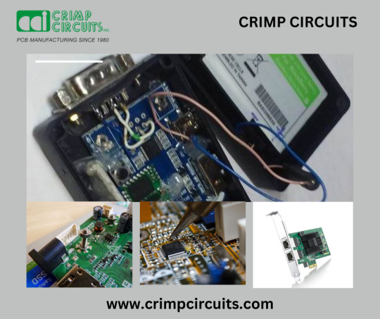
The Journey of PCB Assembly: An Intricate Dance of Precision and Technology
Printed Circuit Board (PCB) assembly is the process of connecting electronic components with the wiring of printed circuit boards. This sophisticated process involves various steps, each crucial for ensuring the functionality and reliability of the final electronic product. From consumer electronics to industrial machinery, PCBs are the backbone of modern technology. In this blog, we will delve into the intricate journey of PCB assembly, highlighting key stages and the technologies involved.
Design and Prototyping
The journey of PCB assembly begins with design and prototyping. Engineers use software like Eagle, Altium Designer, or KiCad to create detailed schematics of the PCB. This design stage involves specifying the locations of components and the routing of electrical connections. The design is then translated into a physical prototype, often through rapid prototyping techniques such as 3D printing or CNC machining.
Material Selection
Selecting the right materials is critical for the performance and durability of the PCB assembly. The board itself is typically made from a fiberglass-reinforced epoxy laminate, known as FR4. The choice of copper thickness, solder mask, and surface finish (such as HASL, ENIG, or OSP) also plays a significant role in the board’s performance and cost.
PCB Fabrication
Once the design and materials are finalized, the PCB fabrication process begins. This involves several steps:
Layering: Multi-layer PCBs are constructed by stacking and bonding multiple layers of copper and insulating material.
Etching: Copper layers are etched to remove unwanted copper, leaving only the desired circuit patterns.
Drilling: Holes for component leads and vias are drilled with precision.
Plating: Holes are plated with copper to ensure electrical connectivity between layers.
Solder Mask and Silkscreen: A solder mask is applied to protect the copper traces, and a silkscreen is added to indicate component locations.
Component Placement
With the PCB fabricated, the next step is to place the electronic components onto the board. This process can be done manually for small-scale or prototype runs, but is typically automated using Surface Mount Technology (SMT) for larger production volumes. Automated Pick-and-Place machines accurately place components onto the PCB at high speeds.
Soldering
After component placement, the components must be securely attached to the board using solder. There are two primary methods for soldering:
Reflow Soldering: For SMT components, solder paste (a mixture of powdered solder and flux) is applied to the board, and then the entire board is heated in a reflow oven. The solder paste melts and solidifies, creating strong electrical and mechanical bonds.
Wave Soldering: For through-hole components, the board is passed over a wave of molten solder. The solder adheres to the exposed metal surfaces, forming connections.
Inspection and Testing
Ensuring the quality and functionality of the assembled PCB is paramount. Various inspection and testing methods are employed:
Automated Optical Inspection (AOI): AOI systems use cameras to inspect the PCB for defects such as missing components or solder bridges.
X-ray Inspection: X-ray machines can inspect hidden solder joints, especially useful for Ball Grid Array (BGA) components.
Functional Testing: This involves powering the PCB and verifying that it performs as expected under operating conditions.
Final Assembly and Packaging
Once the PCB passes inspection and testing, it may undergo final assembly, where additional components such as connectors, heatsinks, or enclosures are added. The completed product is then packaged, ready for shipping to customers or further integration into larger systems.
Conclusion
The journey of PCB assembly is a fascinating blend of design, materials science, precision engineering, and advanced manufacturing techniques. Each stage, from initial design to final testing, plays a crucial role in delivering reliable and high-performance electronic products. As technology continues to evolve, so too will the methods and tools used in PCB assembly, driving innovation and enabling the creation of increasingly sophisticated electronic devices. For more details visit our website www.crimpcircuits.com
#pcb manufacturing toronto#printed circuit board design#metal clad pcb#printed circuits#rigid flex pcb#full turnkey pcb services#turnkey pcb services#pcb parts#eagle software#pcb designing#flexible pcb#pcb assembly#printed circuit board manufacturers#pcb manufacturers in canada#circuit board manufacturers in canada#pcb quote#pcb prototype services in canada
0 notes
Link
Share blog about reflow oven heating curve operation precautions
know more about this problem can click the link
0 notes
Text
Industrial Ovens: What You Need to Know
Industrial ovens are used in a wide range of applications in many industries, specifically to heat materials for uses such as baking, curing, and drying. They may be used in the food processing industry, the chemical industry, or the electronics industry. However, it is necessary to have good knowledge of the types of industrial ovens and their capability so that you can make the right decision for the business. In today’s blog, we will provide you what industrial ovens are, different types, and key considerations before choosing an industrial oven in the UAE, and why you should buy one.
Types of Industrial Ovens
Curing Ovens
Drying Ovens
Baking Ovens
Heat-Treating Ovens
Reflow Ovens
Vacuum Ovens
Things to consider before buying industrial ovens in the UAE
Application Requirements
Energy Efficiency
Size and Capacity
Temperature Control
Compliance with Local Regulations
Maintenance and Support
Purchasing an industrial oven from us is a wise decision. Understanding different types of industrial ovens and key considerations can help you make better-informed decision. We at Oki Bering offer you a perfect platform for purchasing industrial ovens with state-of-the-art features and quality assurance. We are the leading supplier of industrial ovens in UAE apart from welding and safety products. Oki Bering has years of experience in the industry. Call us at +971 48860679 or +971 48860678 to know more.
0 notes
Text
The Role of Soldering in Circuit Card Assembly
Circuit card assembly (CCA) is a critical process in the production of electronic devices, involving the integration of various electronic components onto a printed circuit board (PCB). But what is circuit card assembly without the essential technique of soldering? Soldering plays a vital role in ensuring the reliability, functionality, and durability of the assembled circuit cards. This blog will explore the importance of soldering in circuit card assembly and how it impacts the overall quality of electronic products.
Understanding Circuit Card Assembly
Before diving into the specifics of soldering, it is important to understand what is circuit card assembly. CCA refers to the process of connecting electronic components to a PCB to create a functional electronic circuit. This involves several steps, including component placement, soldering, inspection, and testing. The quality of each step significantly influences the performance and longevity of the final product.
The Importance of Soldering in CCA
Soldering is the process of joining two or more electronic components together by melting solder around the connection. The solder, a fusible metal alloy, creates a strong electrical bond between the components and the PCB. Here’s why soldering is crucial in circuit card assembly:
1. Electrical Connectivity
The primary function of soldering in CCA is to ensure electrical connectivity between components. Properly soldered joints provide a reliable path for electrical signals to travel through the circuit, ensuring that the device operates as intended. Without secure solder joints, components may not function correctly, leading to device failure.
2. Mechanical Stability
In addition to electrical connectivity, soldering provides mechanical stability to the components on the PCB. Solder joints help hold the components in place, preventing them from moving or becoming loose. This stability is particularly important in devices subjected to physical stress or vibration, such as mobile phones and automotive electronics.
3. Thermal Conductivity
Soldering also plays a role in thermal conductivity, helping to dissipate heat generated by the components during operation. Proper heat dissipation is essential for maintaining the performance and longevity of electronic devices. Poor soldering can lead to overheating, which can damage components and reduce the lifespan of the device.
4. Minimizing Signal Interference
Good soldering practices help minimize signal interference in electronic circuits. Poorly soldered joints can create electrical noise and signal degradation, affecting the performance of the device. High-quality solder joints ensure that the electrical signals remain clear and free from interference.
Types of Soldering Techniques in CCA
There are several soldering techniques used in circuit card assembly, each with its advantages and specific applications:
1. Hand Soldering
Hand soldering is a manual process where a technician uses a soldering iron to join components to the PCB. This technique is often used for small-scale production, prototyping, and rework tasks. While hand soldering provides flexibility and precision, it requires skilled technicians to ensure high-quality joints.
2. Wave Soldering
Wave soldering is an automated process commonly used for through-hole components. In this method, the PCB is passed over a wave of molten solder, which creates solder joints for all the components simultaneously. Wave soldering is efficient and suitable for high-volume production, but it may not be ideal for surface-mount components.
3. Reflow Soldering
Reflow soldering is the preferred method for surface-mount technology (SMT) components. In this process, solder paste is applied to the PCB, and components are placed on the paste. The assembly is then heated in a reflow oven, causing the solder paste to melt and form joints. Reflow soldering is precise and ideal for densely packed PCBs.
Ensuring Quality in Soldering
To achieve high-quality solder joints, it is essential to follow best practices in soldering. This includes using the right soldering temperature, ensuring proper flux application, and avoiding common soldering defects such as cold joints, solder bridges, and voids. Regular inspection and testing are also crucial to identify and rectify any issues early in the process.
Conclusion
Soldering is an indispensable technique in circuit card assembly, playing a crucial role in ensuring electrical connectivity, mechanical stability, thermal conductivity, and signal integrity. By understanding what is circuit card assembly and the importance of soldering, manufacturers can produce reliable and high-performing electronic devices. Whether through hand soldering, wave soldering, or reflow soldering, achieving high-quality solder joints is essential for the success of any electronic assembly project.
0 notes
Text
PCB Assembly Board
What is PCB Assembly ?
PCB Assembly manufacturer - Hitech Circuits Co., Limited
It’s the step in the manufacturing process in which you populate a blank board with the electronic components needed to make it into a functional printed circuit board. It’s these components that make a board into the circuit that enables an electronic product to function. PCB assembly typically takes place via one of two processes:
1. Surface-mount technology
SMT: SMT stands for “Surface Mount Technology“. The SMT components are very small sizes and comes in various packages like 0201, 0402, 0603, 1608 packages for resistors and capacitors. Similarly for Integrated circuits ICs we have SOIC, TSSOP, QFP and BGA.
The SMT components assembly is very difficult for human hands and can be time taking process so it is mostly done by automated pick and place machine.
2. Through-hole manufacturing
THT: THT stands for “Through hole Technology”. The components with leads and wires, like resistors, capacitors, inductors, PDIP ICs, transformers, transistors, IGBTs, MOSFETS are example.
The component has to be inserted on one side of PCB and pulled by leg on other side and cut the leg and solder it. The THT components assembly is usually done by hand soldering and is relatively easy.
Printed Circuit Board Assembly Techniques
There are only two common PCBA techniques available for use by a PCB designer. The methods are:
1. Automated PCB Assembly Techniques
Generally, this technique employs the use of state of the art machines, which are fully automatic. For example, the surface mount components are worth positioning with the aid of an automated pick and place machine.
Again, reflow soldering is commonly for surface mount components usually done in a reflow oven. An automated solder stencil is also used to apply the solder paste on the PCB.
Finally, high tech inspection machines are used to confirm and check the quality of the PCBA. Some of which include: Automated optical inspection machine (AOI), X-ray inspection machines, etc.
Above all, due to the precise monitoring, control of soldering, no human input and versatile machines.
This technique ensures utmost efficiency, output consistencies, and limits defects.
2. Manual PCB Assembly Techniques
This method is favorite for use with through-hole parts, which needs manual placement on the board. Besides, with these through-hole parts, it’s advisable you use wave soldering. Note that in the through- hole assembly process, you need to place the components and electronics on the PCB.
After that, you use wave soldering to solder the leads. Typically, you will need an individual to insert a component into a marked PTH. Once done, transfer the PCB to the next station where the next person will be on standby tasked with fixing another part.
WWW.HITECHPCBA.COM
What are the Benefits of SMT PCB Assembly?
SMT assembly provides many benefits and some of them are as follows:
It can be used to incorporate small components.
In SMT, the components can be placed on both sides of the board.
It assures high component densities.
Fewer holes need to be drilled for surface mounting than through-hole.
It require low initial costs and time for setting up the mass production.
SMT is the simpler and faster-automated assembly when compared to through-hole.
Errors regarding the component placement can be easily rectified.
Surface mount PCBs feature strong joints, which can easily withstand vibrations.
What are the techniques used in Surface Mount Technology?
There are several techniques for the reflow process. After applying the solder paste or a flux mixture on the board and after placing the components, the boards are conveyed to a reflow soldering oven. The techniques used for reflowing soldering include infrared lamps, hot gas convection, fluorocarbon liquids with a high boiling point, and so on.
What are the different testing methods used in SMT PCB Assembly?
Hitech Circuits as the PCB assembly manufacturer, we perform the following testing and inspection to ensure the quality of surface mount PCBs.
Automated Optical Inspection (AOI): This is performed before and after the soldering to identify the component placement, presence, and solder quality.
X-ray Testing: In this type of testing, the operator relies on the X-ray images of the PCB to check the solder joints and lead-less components such as Quad Flat Packs and ball grid arrays, which are generally not visible to naked eyes.
In-Circuit Testing (ICT): This method is used to detect manufacturing defects by testing the electrical properties in the SMT Assembly.
What type of files or documents should I send for SMT PCB Assembly?
Gerber Files: The file contains all details of physical board layers including solder masks, copper layers, drill data, legends, and so on.
Bill of Materials (BOM): This contains information on the list of items needed for the PCB manufacturing and the instructions of manufacturing.
Pick and Place File: This file contains information on all components to be used in the PCB design and their rotation and X-Y coordinates.
WWW.HITECHPCBA.COM
The whole process of PCB Assembly
1. Bare board loader machine
The first step in the PCB assembly is to arrange the bare boards on the rack, and the machine will automatically send the boards one by one into the SMT assembly line.
2. Printing solder paste
When PCB on the SMT production line, firstly, we have to print solder paste on it, and the solder paste will be printed on the pads of the PCB. These solder pastes will be melt and solder the electronic parts to the circuit board when it passes through the high-temperature reflow oven.
In addition, when testing new products, some people will use film board/adhesive cardboard instead of solder paste, which can increase the efficiency for adjusting the SMT machines.
3. Solder paste inspection machine(SPI)
Since the quality of solder paste printing is related to the quality of welding of subsequent parts, some SMT factories will use optical machine to check the quality of solder paste after printed the solder paste in order to ensure stable quality. If there any poorly printed solder paste board, we will wash off the solder paste on it and reprint, or remove the excess solder paste if there is redundant solder paste on it.
4. High speed SMT machine
Usually, we will put some small electronic parts (such as small resistors, capacitors, and inductors) to be printed on the circuit board first, and these parts will be slightly stuck by the solder paste just printed on the circuit board, so even if the speed of printing is very fast and the parts on the board will not fall away. But large parts are not suitable for use in such high speed SMT machines, which will slow down the speed of small parts assembly. And the parts will be shifted from the original position due to the rapid movement of the board.
5. Universal SMT machine
Universal SMT machine is also known as "slow machine", it will be assembled some large electronic components, such as BGA IC, connectors, etc., these parts need more accurate positions, so the alignment is very important. Use a camera to take a picture to confirm the position of the parts, so the speed is much slower than High speed SMT machine we taked before. Due to the size of the components here, not all of them are packed in tape and reel, and some may be packed in trays or tubes. But if you want the SMT machine to recognize the trays or tube-shaped packaging materials, you must configure an additional machine.
Generally, traditional SMT machines are using the principle of suction to move electronic parts, and in order to place the parts successfully, and there must be the flat surface on these electronic components for the suction nozzle of the SMT machine to absorb. However, for some electronic parts don’t have a flat surface for these machines, and it is necessary to order special nozzles for these special-shaped parts, or add a flat tape on the parts, or wear a flat cap for thees electronic parts.
6. Manual parts or visual inspection
After assembled all parts by the high speed SMT machine or Universal SMT machine and before going through the high-temperature reflow oven, and we will set up a visual inspection station here and to pick out the deviation parts or missing components boards etc., because we have to use a soldering iron to repair if there are still defectives boards after passing the high-temperature oven, which will affect the quality of the product and will also increase the cost. in addition, for some larger electronic parts or traditional DIP parts or some special reasons cannot be processed by the SMT machine before, they will be manually placed on pcb here.
7. Reflow oven
The purpose of reflow oven is to melt the solder paste and form a non-metallic compound on the component feet and the circuit board, that means to solder electronic components on the circuit board. The temperature rise and fall curves often affect the soldering quality of the entire circuit board. According to the characteristics of the solder materials, usually the reflow oven will set the preheating zone, soaking zone, reflow zone, and cooling zone to achieve the best soldering effect.
For example, the melting point for SAC305 solder paste with lead-free is about 217°C, which means that the temperature of the reflow oven must be higher than the melting points to remelt the solder paste. What's more, the maximum temperature in the reflow furnace should not exceed 250°C, otherwise many parts will be deformed or melted because they cannot withstand such a high temperature.
Basically, after the pcb passed through the reflow oven, the assembly for the entire circuit board is almost complete. If there are hand-soldered parts, we need to transfer to DIP process, and then we have to check the quality after reflow oven by QC department.
WWW.HITECHPCBA.COM
8. Automatic optical inspection(AOI)
The main purpose of setting up AOI is because some high density boards can’t be process the following ICT test, so we used AOI inspection to replace it. But even using AOI inspections, there still have the blind spots for such checking, for example, the solder pads under the components cannot be checked by AOI. At present, it can only check whether the parts have side standing issue, missing parts, displacement, polarity direction, solder bridges, lack of soldering etc., but cannot checking the BGA solderability, resistance value, capacitance value, inductance value and other components quality, so far AOI inspection can’t completely replace ICT test.
Therefore, there is still some risk if only AOI inspection is used to replace ICT testing, but ICT test is also not 100% make sure the good quality, we suggest these two ways can be combined with together to make sure the good quality.
9. PCB unloader machine
After the board is fully assembled, it will be retracted to the unloder machine, which has been designed to allow the SMT machine to automatically pick and place the board without damaging the quality for PCB.
10. Visual inspection for finished products
Normally there will be a visual inspection area in our SMT production line whether there is an AOI station or not, and it will help to check if there are any defectives after completed assembled the pcbs. If there is an AOI station, it can reduce the visual inspection worker on our SMT line, and to reduce the potential cost, and because it is still necessary to check some places that cannot be judged by AOI, many SMT factories will provide the mainly visual inspection templates at this station, which is convenient for visual inspection worker to inspect some key parts and polarity for components.
11. DIP process
DIP process is a very important process in the whole PCBA processing, and the processing quality will directly affect the functional for PCBA boards, so it is necessary to pay more attention to the DIP process. There are many preliminary preparations for DIP process. The basic process is to re-process the electronic components first, like to cut the extra pins for some DIP components, our staff received the components according to the BOM list, and will check whether the material part numbers and specifications are correct or not, and performs pre-production pre-processing according to the PCBA samples. The steps are: Use various related equipment (automatic capacitor pins cutting machine, jumper bending machine, diode and triode automatic forming machine, automatic belt forming machine and other machines) for processing.

12. ICT test
Printed Circuit board open/short circuit test (ICT, In-Circuit Test), The purpose of ICT test is mainly to test whether the components and circuits on the printed circuit board are open or short issues. It can also measure the basic characteristics of most components, such as resistance, capacitance, and inductance values to judge whether the functions of these parts are damaged, wrong parts or missing parts etc. after passing through the high-temperature reflow oven.
ICT test machines are divided into advanced and basic machines. The basic ICT test machines are generally called MDA (Manufacturing Defect Analyzer). It’s just to measure the basic characteristics of electronic components and judge open and short circuits issue we talked above.
In addition to all the functions of the basic ICT test machines, for advanced ICT test machine can also test the whole PCBA by using power, start to testing the PCBA boards by setting the program in the test machine. The advantage is that it can simulate the function of the printed circuit board under the actual power-on condition, this test can partly replace the following functional test machine (Function Test). But the cost for the test fixture of this advanced ICT test can probably buy a car, it’s too expensive and we suggest it can be used in mass production products.
13. PCBA function test
Functional testing is to make up for the ICT test, because ICT only tests the open and short circuits on the the PCBA board, and other functions such as BGA and other fuctions are not tested, so it is necessary to use a functional testing machine to test all functions on the whole PCBA board.
14. Cutting board (assembly board de-panel)
Normally, printed circuit boards will be produced in panel, and it will be assembled to increase the efficiency of SMT production. It means several single boards in one panel, such as two-in-one, four-in-one etc. After finished all the pcb assembly process, it needs to be cut into single boards, and for some printed circuit boards with only single boards also need to cut off some redundant board edges.
There are several ways to cut the printed circuit board. You can design the V-cut using the blade cutting machine (Scoring) or directly manually break off the board (not recommended). For more high density circuit boards, it will be used the professional splitting machine or the router to split the board without any damage the electronic components and printed circuit boards, but the cost and working hours will be a little longer.
Why Choose Hitech Circuits PCB Assembly Manufacturer for Your PCB Assembly Projects?
There are several PCB manufacturers specializing in PCB assemblyservices. However, Hitech Circuits PCB Assembly stands out owing to the following:
Assistance in Material Procurement:
Technically, in PCB assembly services, the quality of parts is the responsibility of the OEM; however, we ease your job by assisting you to make the right selection. We can help you procure all your parts of the same type own a single part number, thanks to our supply chain and vendor network as well as experience. This saves time and cost that goes in ordering single parts as you plan.
Testing procedures:
We are very focused on quality and thus implement stringent testing procedures at each stage of the assembly and after completion.
Fast Turnaround Times:
Our well-equipped facility and the right tools enable us to complete your requirements well before time, and without compromising on the quality or functioning of the PCBs. For simple designs we revert in 24 to 48 hours.
Cost Effectiveness:
While PCB assembly is a cost-effective alternative, we go a step further and assure that the parts you list are of a good quality and suitable for your requirement. Also, you can control the part flow and replenish them as needed. This eliminates the need to buy extra stock and store it.
Quick Quote:
We offer a quick quote based on your BOM. All you need is a detailed BOM, Gerber files, your application requirement sheet, and quantity.
We’re not one to stand still, which is why we use the latest equipment and the finest minds to create your PCB projects. We’re constantly keeping our finger on the pulse of the latest trends. And as a result, we know how to deliver the highest standards of PCB assembly to meet all your requirements.
Our dedicated, friendly customer service team also means that we support you every step of the way. Offering our expert guidance to ensure a complete PCB project that you’re happy with.
Contact us today
No matter what your printed circuit board assemblyneeds are, we always aim to deliver efficient, dependable solutions. For more information about our services, do not hesitate to get in touch with us today for a no-obligation quote
0 notes
Last Seen Blogs

nikehuaracheblackcoolgreys9-blog
nike huarache black cool grey - nike huarache blac

oceanvillavungtau-blog
Ocean Villa Vung Tau

navykove
Indifferentia ad vitam.

notoriouslr
Niner Gang
cikyum
KUNCI HATI