#smd reflow
Link
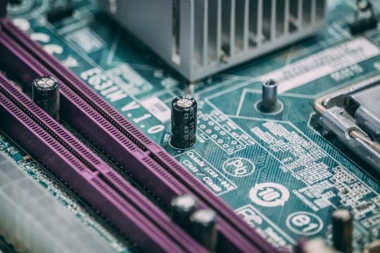
Get the best SMT and SMD Reflow Services in Gandhinagar and Ahmedabad, India. Our experienced team delivers fast, efficient, and high-quality results. Contact us now to get started!
Our services play a crucial role in the production of process control instruments for industrial and commercial applications, such as temperature, pressure, and flow control solutions.
#smd reflow#surface mountain device#smt#electronics manufacturing service#pcb contract manufacturing#pcb assembly#pcb soldering#pcb wave-soldering in ahmedabad#gandhinagar#ahmedabad#electronics industry#electronics in gandhinagar
0 notes
Note
hello i got into doin diy electronics a couple months ago, i got a good solderin iron but those reflow stations look fire. do u have a rec for a good one that dont break the bank? doin smd stuff w/ a iron kinda sucks
I think I have this one:
It's a clone of one of the better ones (A Hakko, I think?)
Not the best, kinda cheap, but it works just fine for what I need.
23 notes
·
View notes
Text
Factors driving the growth of SMT PCB assembly in India
The electronics manufacturing industry of INDIA has shown a lot of growth in the recent years. India is soon coming up as electronics manufacturing destination with strong supply chain and skilled manpower acting as the catalysts. SMT PCB assembly is a standout technique that can exceptionally engage in electronics manufacturing, typically in Printed Circuit Board assembly.
SMT PCB Assembly is the process of placing electronic components onto the surface of the printed circuit board (fused with PCB). This new technology does away with the through-hole process where parts are inserted directly into drilled holes. SMT also enables the Manufacture of smaller and lightweight components which go well with the current small electronic gadgets that require improved performance.
Components
Surface Mount Devices (SMDs): These are the components that are screwed onto the circuit board surface such as resistors, capacitors, diodes, and integrated circuits.
Solder Paste: A combination of powder solder and a flux which is needed to hold the SMDs in position while in the PCB.
Pick-and-Place Machines: Special machines that are capable of correctly positioning SMDs on the PCB that has solder paste on it.
Reflow Oven: Used to heat the PCB and melt the solder paste to give strong connection between the SMDs and the PCB.
Factors
The electronics industry in India has also benefited from enormous economic growth over the last few decades. The drastic increase of SMT PCB assembly in India can be attributed to several factors in its economical aspect. Some of the most important factors include the development of sound government policies and incentives aimed at enhancing electronics manufacturing within the country. Rising internal consumption towards electronics and related products has played a key role in the growth of SMT PCB assembly in India.
The most important strength of the country is the demography factor which offers a large number of youths and qualified technical workforce. This skilled labor force is a valuable benefit because it contributes to the rate of increase and improved effectiveness of SMT PCB assembly in India.
To improve the skills of this competent workforce, various training schemes and interventions have been developed. Various government initiatives like the Skill India Mission and the Electronics System Design and Manufacturing (ESDM) program ensures that people are skilled in modern electronics manufacturing processes.
Several educational institutions prepare talent for SMT PCB assembly in India and these institutions are crucial to its growth. Smt Pcb Assembly has special modules included in the engineering colleges and technical institutes that focus on manufacturing electronics with electronics manufacturing courses.

Epsilon electronics emerges as the industry leader of SMT PCB Assembly in India that relies on the best technology and on the strict fulfillment of the highest quality standards. Epsilon Electronics offered efficient SMT PCB assembly solutions which improved the value of its communication devices. Epsilon Electronics has a big share in the SMT PCB Assembly in India along with many successful project work and good vision.
#SMT PCB Assembly in India#ems solution provides#pcb assembly service provider#pcb assembly service provider in gujarat#pcb assembly service provider in india#pcb design company in gujarat#circuit design company in india#ems solution provider#pcb design company in india#ems supplier in gujarat#ems supplier in india
0 notes
Text
Through Hole PCB Assembly
THT PCB Assembly Manufacturer – One-stop service
What’s mean for Through Hole (THT) PCB Assembly and Surface Mount Technology(SMT)PCB Assembly ?
Surface Mount Technology (SMT) is necessary for PCB assembly. If the PCB has no through-hole components, Through Hole (THT) PCB Assembly is not needed.
SMT assembly: SMT stands for surface mount technology, which is a versatile PCB assembly technology. Currently, all electronic components can be made into surface-mounted devices (SMD). SMDs are interconnected to the PCB pads with solder paste. SMT assembly is automatic.
THT assembly: THT, or PTH or DIP, means through-hole technology. The electronic components that require THT assembly have long pins. Usually, they are capacitors, fuses, and connectors. The PCB is pre-drilled, and these components' pins plug in the holes and wave reflowed. THT assembly is manual.
In the PCB assembly process, SMT assembly happens before the THT assembly.

What are the benefits of Through Hole PCB assembly?
Through-Hole PCB Assembly comes with a range of benefits including:
Withstanding stress-As opposed to SMT components, through-hole components are known for their ability to withstand mechanical and environmental stress.
Perfect for large components-Through-hole works well for large components that have to undergo high power and high voltage
High heat tolerance-Known for their high heat tolerance, they find application in a number of industries, particularly military and aerospace.
Ease of Prototyping- Through-hole PCBs also lend themselves to ease of prototyping and improved reliability
High Reliability-Through-hole PCBs are best used for high-reliability products that require stronger connections between layers.
Little surprise then, that even though surface mount components allow for denser configurations, for larger and heavier components that require strong bonds, through-hole technology has remained resilient and relevant.
What are the capabilities you offer for Through Hole PCB assembly?
We provide through-hole PCB services to a variety of industries including medical, electronics, instrumentation, and military, all thanks to our complete assembly capabilities:
• Hand soldering
• Dual wave flow solder
• Hand Insertion of components
• Automate axial or radial insertion
• RoHS soldering using tin-lead solder
• Use of high and low melting point solder
• Prototype build to high-volume assembly
• Functional test and automated inspection
• Support various types of PCBs including metal core PCBs, Rigid PCBs, Flex-rigid PCBs, FR4 PCBs, etc.

Disadvantages of Through Hole Assembly
Like any other manufacturing or assembling techniques, Through Hole PCB Assembly has its disadvantages too.
These include:
Longer production time-It takes a lot of time to drill the multiple holes through which the leads are expected to run.
Expensive-because the drilling process is difficult and time-consuming, it increases the cost of production
Minimizes space on the boards-drilling the holes on the surface of the board limits the routing area for tracing signals.
Also, by feeding the leads through the board, only one of its sides is usable, thus making the THT PCB a bit slower in operation speeds.
Through Hole Assembly Components – What are the Best Components for Through Hole Assembly?
Radial lead components
Axial lead components.
Types of Through Hole PCB Assembly
There are two (2) main types of the Through Hole PCB Assembly. The first is the Automated Through Hole PCB Assembly. The second is the Manual Through Hole PCB Assembly.
On the one hand, the automated variant is roundly touted to be faster and cost-effective because it takes little time to be completed. It also demands little human inputs, which makes it cost-effective.
On the other hand, the manual Through Hole PCB Assembly involves the traditional or manually-operational model of drilling the holes into the Printed Circuit Boards (PCBs). This model tends to take time and attracts more costs.
Functional tests and automated inspection for Through Hole PCB Assembly
Using automated inspection is very critical in minimizing turnaround time to ensure timely delivery of the boards.
Conclusion
As you can see, Through Hole Assembly of PCB can be time consuming.
However, in some applications, it is worth it more so when mounting heavier and bulkier components.
You can easily achieve the strength by soldering the components on the reverse side as you have seen.
In fact, it is virtually impossible to pull components assembled using Through Hole Assembly.
The good news, today’s guide has simplified the Through Hole PCB Assembly technique.
Do you have questions or inquiries on Through Hole Assembly process?
Contact us now. [email protected]

In addition to through hole PCB assembly, we also provide value-added services, such as conformal coating, labeling, and complete PCB encapsulation.
Through-hole PCB Assembly Testing and Inspection at Hitechpcba
In-Circuit Testing:
This type of testing is conducted for high volume production lines, and helps us check every minute soldering and other components in detail.
Automated Optical Inspection: Abbreviated as AOI, these tests are performed to ensure that product is free from soldering, component, and BGA defects.
Automated X-Ray Inspection(AXI):
This testing is performed to inspect insufficient fills, short circuits, fills, etc. The automated X-ray inspection helps reduce the number of defects and improve the quality of the Through-Hole circuit.
Burn-in Tests:
These tests detect components’ failure or reliability in real environments.
Assisted Visual Inspection:
Our experts use a wide range of advanced visual inspection equipment to perform a detailed inspection of soldering and component placement accuracy.

What’s difference between SMT assembly and THT assembly?
Most contract PCB Assembly manufacturers concentrate on their surface mount technology capabilities for PCB assembly. The SMT lines can be almost completely automated making it possible to run a high volume of boards with little human intervention and a low cost per board. Through whole assembly whether automated or manual is a slower process, it takes resources away from the high-volume business that many manufacturers prefer.
Only about 10 percent of the parts we buy are through-hole. Nearly 75 percent of the boards we run are mixed technology, which is a combination of through-hole and SMT parts one reason for this is that nearly half of our board assemblies are for high powered boards which use capacitors inductors and transformers to transfer energy. The size of these components is proportional to the energy they can store so for a high-power board we need to use some fairly large and heavy components and that means through-hole technology, in addition things like customer accessible connectors, that have to withstand stress as cables are connected and removed are likely to be through-hole components. Through-hole components are held in place by the pins as well as the solder so you can get a much stronger and more reliable mechanical bond than with surface mount components that have only solder to hold them in place. If a contract manufacturer is focused on higher volume SMT business, it's important to understand how they will handle through-hole components when you need them at z-axis. We run mixed technology boards every day we have a modern stuff line with a paperless process for assembly instructions and assemble in a single piece flow from the stuff line to a wave solder to inline inspection, d-paneling, qc testing.
In addition to PCB Assembly, be it through hole or surface mount, at Hitech Circuits Co., Limited we also undertake PCB assembly rework offering complete reliability, high quality and optimal costs. Not only are we well-versed in inventory management, fabrication and process control, we also have a stringent control on vendor component management.
0 notes
Text
SMT production process

Program the SMT placement machine
According to the BOM position map provided by the customer, program the coordinates of the location of the components. Then carry out the first piece with the SMT chip processing data provided by the customer.
Printing solder paste
The solder paste is stenciled to the PCB board where the electronic component SMD needs to be soldered to prepare for the soldering of the components. The equipment used is a screen printing machine (printing machine), which is located at the forefront of the SMT chip processing production line.
SPI
Solder paste detector, detects whether the solder paste printing is a good product, whether there is less tin, leaking tin, more tin and other undesirable phenomena.
4.SMT
Accurately install the electronic components SMD on the fixed position of the PCB. The equipment used is a placement machine, which is located behind the screen printing machine in the SMT production line.
The placement machine is divided into high-speed machine and general-purpose machine.
High-speed machine: used to paste components with large pin spacing and small pin spacing
Universal machine: paste small pin pitch (pin density), bulky components.
High temperature solder paste melting
Mainly, the solder paste is melted at high temperature, and after cooling, the electronic components SMD and the PCB board are firmly welded together. The equipment used is a reflow soldering furnace, which is located behind the placement machine in the SMT production line.
AOI
Automatic optical detector to detect whether the soldered PCBA components have poor soldering, such as tombstone, displacement, empty soldering, etc.
Visual inspection
The key items of manual inspection and inspection: whether the PCBA version is the changed version; whether the customer requires components to use substitute materials or components of designated brands and brands; IC, diodes, triodes, tantalum capacitors, aluminum capacitors, switches, etc. Whether the direction of the directional components is correct; defects after welding: short circuit, open circuit, fake parts, fake welding.
Packaging
Products that have passed the test will be packaged separately. The commonly used packaging materials are anti-static bubble bags, electrostatic cotton, and blister trays. There are two main packaging methods, one is to use anti-static bubble bags or electrostatic cotton into rolls, which are the most commonly used packaging methods at present; the other is to customize blister trays according to the size of PCBA. Put it in a blister tray and unpack it, mainly for PCBA boards that are sensitive and have vulnerable patch components.
0 notes
Text
SMD Dizgi Nedir?
Yüzey Montaj Teknolojisi (SMD), elektronik komponentlerin pcb üzerine yüzey üzerine monte edildiği bir üretim yöntemidir. Bu teknoloji, geleneksel delik montajından farklı olarak daha küçük boyutları, yüksek yoğunluğu ve hafifliği beraberinde getirir. SMD dizgi süreci, pasta baskı, komponent yerleştirme, lazer kontrol ve reflow lehimleme adımlarını içerir. Yüksek entegrasyon, daha kompakt…

View On WordPress
0 notes
Text

Reflow soldering station:This station mainly consists of reflow oven. The soldering of SMDs is to make PCBs with components mounted on them pass reflow oven with soldering parameters set to implement components soldering.
#pcb#pcba#pcblayout#pcbfabrication#pcbdesign#pcbassembly#SMT#DIP#BGA#electronics#component#USB#ledboard#aluminum#pcbboard#IC#power#supply#Bluetooth#HDI#sports#headset
0 notes
Text
Surface Mount Technology Market Insight, Size, Share and SWOT Analysis by Key Players, Forecast 2030
Surface Mount Technology (SMT) revolutionizes electronic assembly by directly mounting components onto PCBs, eliminating the need for through-hole insertion. This method enhances device compactness, weight reduction, and component density, making it the preferred choice in contemporary electronics manufacturing.
Market Dynamics: The Surface Mount Technology market has witnessed rapid expansion owing to the escalating demand for compact, lightweight, and high-performance electronic devices across diverse industries. The surge in smartphones, tablets, wearable tech, IoT devices, and automotive electronics has propelled the adoption of SMT solutions. Additionally, advancements in SMT equipment, materials, and processes have bolstered productivity, yield rates, and cost-effectiveness, further amplifying market growth.
Request Sample Report: https://www.snsinsider.com/sample-request/3433
3. Key Components and Technologies:
The Surface Mount Technology market encompasses a wide range of components, equipment, and materials tailored to meet the diverse needs of electronics manufacturers. Key components include surface mount devices (SMDs) such as resistors, capacitors, diodes, integrated circuits (ICs), and microcontrollers. SMT equipment includes pick-and-place machines, solder paste printers, reflow ovens, and inspection systems. Materials such as solder paste, solder masks, and adhesives play a crucial role in the SMT process.
4. Market Segmentation:
The Surface Mount Technology market can be segmented based on component type, equipment type, application, and geography. Component types include passive SMDs, active SMDs, and electromechanical components. Equipment types encompass placement machines, soldering equipment, inspection systems, and cleaning systems. Applications range from consumer electronics and telecommunications to automotive, aerospace, medical devices, and industrial equipment.
5. Future Outlook:
The future of the Surface Mount Technology market looks promising, with continued advancements in miniaturization, automation, and smart manufacturing driving innovation and market expansion. The rise of Industry 4.0 and the Internet of Things (IoT) is expected to further accelerate the adoption of SMT solutions, as manufacturers seek to improve efficiency, flexibility, and connectivity in their production processes. Moreover, the increasing demand for electric vehicles, renewable energy systems, and smart infrastructure will create new opportunities for SMT technology providers.
Conclusion:
In conclusion, the Surface Mount Technology market is at the forefront of electronics manufacturing, enabling the production of smaller, lighter, and more advanced electronic devices. As the demand for high-performance electronics continues to grow, SMT solutions will play an increasingly critical role in driving innovation and competitiveness across industries. With ongoing advancements in technology, materials, and processes, the Surface Mount Technology market is poised for sustained growth and innovation in the years to come, shaping the future of electronics manufacturing.
Access Full Report Details: https://www.snsinsider.com/reports/surface-mount-technology-market-3433
0 notes
Text
Unveiling the advantages and disadvantages of Surface Mount Technology (SMT)
Introduction
Printed circuit board assembly, in particular, has significantly benefited from surface mount technology (SMT). SMT eliminates the requirement for drilled holes and manual insertion by mounting electronic components directly onto a PCB's surface. This technique offers several advantages, such as smaller and thinner PCBs, flexibility in design, reduced material costs, simplified automation, and high signal transmission capabilities.
Advantages of SMT in PCB Assembly
Ultra-Thin and Miniature PCBs
The size and weight of surface-mount components are significantly lower than their through-hole counterparts. Boards are smaller and thinner because their compactness makes better use of space on printed circuit boards. As a result, products can be designed to be more compact without compromising functionality or performance.
Flexibility
SMT provides great flexibility in terms of PCB materials and designs. It enables the use of flexible PCBs (flex PCBs) and rigid-flex PCBs that can bend or conform to specific shapes or spaces. This flexibility opens up opportunities for innovative designs while maintaining excellent electrical performance.
Lesser Expense on Materials and Cardboard
Unlike through-hole components that require manual insertion, SMD components can be automatically placed on the board using pick-and-place machines or automated assembly lines. This automation streamlines the production process, reduces labour costs, and improves efficiency.
Simplified Manufacturing Process
When compared to through-hole components, surface-mount devices (SMDs) can be automatically positioned on the board through the use of pick-and-place machines or automated assembly lines. Because of this automation, production is more streamlined, costs less to operate, and more efficient overall.
Frequency and High Signal Transmission
Fast signal transmission with less radio frequency interference is made possible using SMT components, which are compatible with high-density double-sided and multi-layer printed circuit board assembly. Additionally, SMT assemblies' lack of leads improves their resilience to vibration and guarantees dependable signal integrity.
Drawbacks of SMT for PCB Build-Up
High Initial Investment
Implementing SMT assembly requires investment in specialized equipment such as reflow ovens, solder paste screen printers, pick-and-place machines, and hot air rework stations. These machines can be costly but are essential for efficient and accurate assembly.
Difficult to Inspect
Due to the small sizes and numerous solder joints of most SMD components, inspection becomes challenging. Identifying defects or faults can be time-consuming, especially when dealing with complex packages like ball grid arrays (BGAs), where solder balls are located under the component.
Fragility
Comparing surface-mount components to their through-hole counterparts, SMD parts are more delicate and fragile. They can be easily damaged if mishandled or dropped during the manufacturing process or while in use. Special care must be taken to handle and package these components using anti-static measures in clean room environments.
Expensive Small Batch Production
Technical complexity necessitates skilled operators and specialized equipment, making prototyping or small-batch manufacture of SMT PCBs an expensive ordeal. Due to the high initial setup expenses, SMT technology may not be cost-effective for small volumes.
Limited Power Capabilities
Surface mount technology isn't suitable for all electrical components, active or passive, because of power constraints. Components generating high heat may not be suitable for surface mounting as it can cause solder melting and compromise the integrity of the connection.
Despite these challenges, SMT remains a highly recommended practice in the manufacturing industry due to its numerous benefits. It enables manufacturing efficiency, design flexibility, better performance in harsh conditions or high-frequency applications, and more compact devices without compromising functionality or performance attributes. With ongoing advancements and innovations in SMT technology aimed at addressing existing limitations and improving production processes further, we can expect to see continued growth and impact on the industry.
This Blog Originally Posted Here: https://www.pcbpower.us/blog/unveiling-the-advantages-and-disadvantages-of-surface-mount-technology
0 notes
Text
youtube
Abracon Proant Stamped Metal Antennas
https://www.futureelectronics.com/m/abracon . Abracon OnBoard SMD antennas are surface mounted sheet metal antennas based on the PIFA (Planar Inverted-F Antennas) technology. It requires no GND cutout and is well suited for efficient mass production by pick and place/reflow soldering. https://youtu.be/QsPokFNqE3M
#Abracon Stamped Metal Antennas#Abracon#Proant#Stamped#Metal Antennas#Stamped Metal Antennas#antennas#Abracon antennas#OnBoard SMD antennas#sheet metal#PIFA#Planar Inverted-F#connectivity#wireless application#Youtube
0 notes
Text
Uncovering the Secrets of Electronic Component Storage
Introduction
Electronic components are the key support for the development of modern science and technology, and their preservation is vital for engineers, electronics enthusiasts and technology enterprises. Nowadays, whether in the global or Chinese market, the rapid growth in the sales of new energy vehicles and intelligent vehicles will drive a new peak in the demand for chips. The actual situation of chip production now is that, on the one hand, chip manufacturers continue to enhance production capacity, and the production situation is gradually improving; on the other hand, the demand for chips is strong, and there will also be a shortage of supply.
Many consumers, however, are unaware that proper storage procedures and environmental conditions can increase the life of components and maintain their performance consistent. We will reveal the mysteries of electronic component storage and teach you how to scientifically preserve these valuable technological gems - electronic components - in this post.
Factors Affecting the Storage of Electronic Components
Each component has its own characteristics, in which the key factors affecting its storage time is the chemical reaction with moisture, oxygen, sulfur and other impurities in the air, as well as temperature, such as electrolytic capacitors in a high-temperature environment electrolyte will dry up and so on. If the vacuum packaging, in a constant temperature environment, electronic components storage time is quite long. Place: Ventilation, dry, no corrosive gas. Warehouse to maintain ventilation, light, ventilation, access to a smooth state, smoking is strictly prohibited, prohibit unauthorized use of fire, electricity and do a good job of fire prevention, fire signs clear.
Storage conditions and duration
A. No special requirements for qualified raw materials, semi-finished goods storage conditions: sunshade, room temperature, ventilation, dry.
B. Storage period
① The effective storage period of electronic components is 12 months;
② plastic parts of the effective storage period of 12 months;
③ The effective storage period of hardware is 6 months;
④ The effective storage period of packaging materials is 12 months;
⑤ The effective storage period of finished products is 12 months.
C. special requirements of the goods for special requirements of the materials stored in accordance with the storage requirements. Material category storage relative temperature storage relative humidity storage height, container storage period solder paste, glue class 2-10 ℃ constant temperature and humidity cabinet storage according to the shelf life of electronic components 20 ± 5 ℃ 40% ~ 70%.
The combination of storage temperature and humidity is the decisive factor. The combination of high humidity and high storage temperatures can cause components to absorb moisture or gases, even if stored for a short period of time.
For SMDs (Surface Mount Devices), moisture sensitivity is measured by the Moisture Sensitivity Level (MSL) defined by JEDEC standard J-STD-020:
MSL Rating Exposure Time Ambient Conditions
Unlimited 30°C/85%RH
1 year 30°C/60%RH
4 weeks 30°C/60%RH
68 hours 30°C/60%RH
72 hours 30°C/60%RH
48 hours 30°C/60%RH
24 hours 30°C/60%RH
TOL 30°C/60%RH
The "exposure time" is the time available after the sealed moisture-proof bag is opened, i.e., components can be reflowed without the risk of "popcorn phenomenon". If the device absorbs moisture during the exposure time it will turn into vapor in the hot oven causing the device to crack, delaminate or even explode. If the exposure time of a component exceeds the specified time, it needs to be "pre-baked". In other words, the device is placed in a drying oven to evaporate the absorbed moisture before use.TOL refers to the "Time of Labeling" indicated by the reference manufacturer.
2.1 Environmental Requirements:
Electronic components must be stored in a clean, ventilated, non-corrosive gases in the warehouse class indoor environment, the warehouse should be in the channel in a smooth state. Another storage of electronic components warehouse temperature and relative humidity must meet the following requirements: temperature: -5-30, relative humidity: 20%-75% RH, the warehouse environment temperature and humidity values will directly affect the storage life of electronic components and quality of quality.
The storage of electronic components has strict requirements for environmental temperature and humidity parameters.
2.2 Special Requirements:
2.2.1. electrostatic sensitive devices (such as MOS field effect transistors, gallium arsenide field effect transistors, CMOS circuits, etc.), should be stored in the storage equipment with the role of shielding static electricity;
2.2.2. Sensitive to magnetic fields but no magnetic shielding of its own electronic components, should be stored in the role of shielding magnetic field storage equipment;
2.2.3. Electromechanical originals with oil seals shall keep the oil seals intact.
Determination of the limited storage period of electronic components: the limited storage period of electronic components in accordance with the Appendix
2.3 Limited Storage Period :
Different grades of electronic components stored in the appropriate temperature and humidity parameters are not the same. class A device storage temperature and humidity values are: 15-25, 25%-60% RH; class B device storage temperature and humidity values are: -5-+30, 20%-75% RH; class C device storage temperature and humidity values are: -10-+40, 10%-80% RH.
2.4 Storage Requirements:
2.4.1. The electronic warehouse requires an anti-static floor, personnel must be in accordance with the requirements of anti-static, dressed in anti-static clothing, wearing anti-static bracelets;
2.4.2. Requirements according to the category of items stored in zones, flammable and explosive products require appropriate isolation measures, for special requirements of the items should have a significant warning signs or safety signs;
2.4.3. The materials are neatly arranged, and the contents of the storage cards are standardized, so that the accounts, materials and cards are in line with each other;
2.4.4. Items can not be stored directly on the ground, need to have a tray or shelf protection;
2.4.5. Material stacking requirements on the small under the big, light under the heavy, a tray can only be placed on the same kind of material, stacking height has special requirements based on special requirements stacking, but the highest shall not exceed 160cm;
2.4.6. Bulk materials, tray materials and items with special requirements for storage specific reference to the relevant norms;
2.4.7. The items with anti-static requirements must be selected according to the actual situation of the following methods: loaded into anti-static bags and anti-static moisture-proof cabinet storage.
2.5 Raw Material Protection Requirements:
2.5.1. Electronic components should give full consideration to the requirements of dust and moisture resistance;
2.5.2. For vacuum-packed PCB light board, IC, etc. to be intact packaging, can not let the copper foil and pins directly exposed to the air to prevent product oxidation;
2.5.3. For the protection of special raw materials, please protect them according to their requirements;
2.5.4. For components with pins, especially IC and other components whose pins are easy to be deformed, we should use the original packaging form to avoid the deformation of the component pins, which may cause inconvenience or even prevent the operation.
2.6 Ambient Temperature and Humidity Requirement
Temperature is a factor we want to discuss in detail. The effects of temperature Cycling of ambient temperatures also causes microcracks and seal failures. If a device is manufactured in a warm and humid climate and then shipped in the cargo hold of an airplane at -40°C, any internal moisture will break the seal as the ice expands. Devices go through different flight or road traffic distribution centers, so they may go through several thaw/freeze cycles before reaching their final destination, causing the malady to continue to grow. If the device then undergoes several winter and summer rotations in a non-temperature-controlled warehouse, less intense but more prolonged thermal cycling stresses may occur.
Assuming that the manufacturer states that the device can be stored in a temperature and humidity range of -40°C to +85°C and 50% RH, this does not mean that the device is safe from several temperature cycles within the storage temperature limits. The fact is that if the device is stored at low temperatures in order to minimize the aging process of the ions or atoms (Figure 3), it must be very slowly rewarmed before use. Continuous storage at low or high temperatures is more suitable for the storage of the components than several hot and cold cycles.
What happens if the storage temperature is exceeded? SMD devices mounted on PCBs do not have the same thermal expansion or contraction as the substrate itself, so mechanical stresses at extreme temperatures can cause solder to break or devices to rupture. Packaged components (diodes, transistors, etc.) can usually withstand lower temperatures because the housing provides mechanical support for the pins, but they generally have metal leadframes, and copper has a high coefficient of thermal contraction, so failures can occur at temperatures below -40°C.
At very low temperatures, the most difficult problems arise in devices that rely on ionic motion or liquid chemical processes, including electrolytic capacitors and some types of ceramic capacitors, because these activities are "frozen" at low temperatures.
Other devices sensitive to very low temperatures are wire-wound inductors and transformers. The copper windings in these devices will shrink at low temperatures and exert mechanical strain on the ferrite core, which becomes more fragile at low temperatures because the adhesive of the ferrite grains loses its elasticity. If a product containing a ferrite device is accidentally dropped at low temperatures, even if it is "securely" encapsulated in an adhesive sealer, it can be easily ruptured by mechanical shock (Figure 4), so care should be taken in handling products and accessories taken out of cold storage.
In summary, if a device or accessory is stored in a good environment that is relatively stable or slow to change, the shelf life is very long indeed. Under ideal conditions, RECOM's encapsulated DC/DC or AC/DC power modules have a shelf life of ten years. However, if such a product is put into service after a long period of storage, it should first be allowed to slowly acclimatize to room temperature and visually inspected to ensure that the pins and connectors are free of corrosion. If the product contains electrolytic capacitors, a limited amount of current should be applied to slowly power up the product (a process known as "reconfiguration") and allow the dielectric insulation of the aluminum oxide to recover before subjecting it to full input voltage.
Global supply chain issues nowadays have resulted in many distributors and suppliers needing to ship out old inventory to meet customer demand in a timely manner. With proper storage conditions and slow warming before power up, these components may still be in perfect condition for use.
Clck to browse More content
1 note
·
View note
Text
youtube
[ENG] DIY SMD reflow hot plate | Arduino project
0 notes
Text
Price: [price_with_discount]
(as of [price_update_date] - Details)
[ad_1]
This Mcare Amtech Soldering paste is good quality solder paste for soldering small SMD components in a reflow oven or with a hot air soldering station. comes in a small container for prototyping or repairing job. This paste is the replacement for solder wire used in Through-hole soldering, some times solder flux is referred to as solder paste. This solder paste comes in a special container, when it is sealed, it can survive for 6 months. If you open the container and want to store the rest of the paste for future use make sure it is tight and place it in a plastic zipper pouch and place it in the refrigerator.
This solder paste for soldering small SMD components in a reflow oven or with a hot air soldering station. comes in a small container for prototyping or repairing job. 100% brand new and effective quality.
Function: repair of mobile phone chips, computer and digital services industries, high-precision circuit board SMT welding, BGA welding process, etc.
If you open the container and want to store the rest of the paste for future use make sure it is tight and place it in a plastic zipper pouch and place it in the refrigerator.
Tin cream for BGA mechanical lead-free welding flux paste for BGA soldering station.
[ad_2]
0 notes
Text
Best PCBA Manufacturing Equipment Services in India
PCB is a Printed Circuit Board. It's a significant electronic part, which is a help for electronic parts and a transporter for electrical associations between electronic parts. As it is created by printing the expected picture on the substrate, it is known as a "printed" circuit board. It's most usually produced utilizing copper-clad epoxy sap/glass material compound.
The PCB is frequently comprised of various layers with 4 and 6 being the most normally utilized, depending on the necessary number of sign layers.
At the point when countless PCBs must be made, odds are parts will not be physically bound manually. This is where proficient gathering houses like Seeed will step in, to assist with manufacturing both the uncovered sheets and collect every one of the parts onto the Printed Circuit Boards, or PCBs.
Best PCBA Manufacturing Equipment Services in India - Syrma SGS
Yet, have you at any point thought about how your makers can stick that monstrous number of small parts onto your PCBs? I have, yet that was until I needed to drive through passages of specialized language online about the apparatus that takes care of business. While there's nothing provocative about PCBA producing, understanding how the cerebrums of all hardware are made most certainly gives pleasure and a feeling of achievement. Heaps of thought go into each phase of the gathering system to convey an entirely working board. Furthermore, with the gadgets getting increasingly progressed, the hardware used to make PCBs are steadily improving and more energizing than at any other time.
Best PCBA Manufacturing Equipment Services in India - Syrma SGS
In PCB gathering, there are 4 primary phases of SMT, or Surface Mount Technology get together utilizing the reflow strategy, which are glue application, mechanized part situation, binding, and review. The essential gear expected for PCB gathering incorporates:
Bind Paste Printing machine
Bind Paste Inspection (SPI) machine
Stick Dispensing machine
Pick-and-Place machine
Reflow Soldering machine
Wave Soldering machine (for through-opening parts)
Programmed Optical Inspection (AOI) machine
In-Circuit Test (ICT) Fixture
Practical Validation Test (FVT) Fixture
Best PCBA Manufacturing Equipment Services in India - Syrma SGS
Bind Paste Printing Machine
The initial phase in PCB gathering is the use of bind glue onto the board. Bind glue is a dim shaded goo produced using a combination of minuscule particles of metal compounds; normally of tin, lead, and silver. Consider it a paste that will keep your finished board intact. Without it, parts wouldn't adhere to your uncovered board.
Patch glue (left), PCB stencil laser-cut openings (right)
Before the glue is applied, a PCB stencil is set over the board. A PCB stencil is a tempered steel sheet that has little laser-cut openings that permit patch glue to be applied exclusively to the region of the board where the parts contacts will ultimately sit on the completed PCB, for example, the SMD cushions.
During the use of patch glue, the PCB stencil and the PCB are gotten into a place in the mechanized glue printer. A wiper then, at that point, applies without lead weld glue on the cushions in exact sums. The machine then hauls a cutting edge across the stencil, to spread and store the glue equitably in the ideal regions. After the stencil is taken out, the patch glue will be precisely where we maintain that it should be (ideally).
Best PCBA Manufacturing Equipment Services in India - Syrma SGS
Weld Paste Inspection (SPI) machine
Various industry studies have brought up that up to 70% of SMD binding issues are followed back to inappropriate or inadequate patch glue printing. Thus, the subsequent stage is to check to assume that the binding glue is printed appropriately onto the board. While utilizing great bind glue printing strategies are in many cases enough for PCBs in low volumes, SPI ought to be thought about while producing higher volumes of PCB to stay away from high modification costs.
0 notes
Text
SMD Inductors Explained
SMD inductor / SMD power inductor, this SMD inductor is also known as power inductor, high current inductor. SMD inductor is the property of closed circuit. When the current flows through the coil of the SMD inductor, SMD inductor in the coil to form a magnetic field induction, induction magnetic field also generates induction current, resistance to the current flowing through the coil. SMD inductors in the circuit to play a role in the passage of non-stationary current to produce a changing magnetic field, and this magnetic field will in turn affect the current, SMD inductors in the power circuit in series such as inductors, inductors on DC is straight through, the high-frequency pulse is highly resistive, so play the role of through DC block AC pulse.

SMD power inductor advantages.
(1) surface mount high power inductors
(2) with miniaturization, high quality, high energy storage and low resistance characteristics
(3) Mainly used in computer display boards, notebook computers, pulse memory program design, and DC-DC converters
(4) Available in reel packaging for automatic surface mounting.
SMD power inductor product features.
(1) Low DC impedance and high allowable current due to original construction and coil technology
(2) Automatic surface loading application
(3) Excellent solderability and environmental resistance
(4) Applicable to reflow soldering
(5) European RoHS compliant products
(6) Lead-free terminals included
SMD power inductors main parameters.
(1) Error / accuracy
(2) Inductance value: the value of the power inductor tested at the frequency of 100Khz. So the brand different inductance value is also different
(3) Self-resonant frequency: The frequency point where the inductance and the rich inductance form a resonance. So in the application, do not exceed the self-resonant frequency to use
(4) DC inductance: wirewound inductance DCR value is larger will lead to heat
(5) Saturation current: The current value when the inductance value drops by 30%
SMD power inductor properties.
SMD inductor, a property of the closed circuit. When the SMD inductor coil through the current, SMD inductor in the coil to form a magnetic field induction, induction magnetic field will in turn generate induction current to resist the current through the coil. SMD inductor in the circuit is through the non-constant current when the role of magnetic field changes, this magnetic field in turn affect the current, SMD inductors in power circuits such as inductors, inductors directly to DC, high-frequency pulse is high resistance, so play a DC resistance AC pulse.
Resistors are used to control the current in the circuit, capacitors are used to isolate the direct current AC, inductors are used to block high frequency through low frequency, on the other hand, capacitors and inductors are energy storage components, so there is also a filtering role in the circuit. Chip inductors in power supply circuits have the characteristics of blocking AC current and allowing DC power to be successfully based. The characteristics of inductors are to pass DC and block AC, the higher the frequency, the greater the characteristic impedance of the electromagnetic coil. Inductors in power supply circuits often work together with capacitors in.
Inductive coils have the characteristic of blocking the change of current in the AC circuit. Inductive coils have similar characteristics to the mechanics of inertia, in electricity named "self-induction", SMD inductors at low frequencies, inductors generally show inductive properties, both only up to storage, filtering high-frequency characteristics, but at high frequencies, its impedance characteristics are very obvious. There is energy consumption and heat, inductive effects reduce the phenomenon. The high frequency characteristics of different inductors are not the same.
SMD power inductor role.
SMD inductor, is an electromagnetic induction element made by winding insulated wires. It is a commonly used inductive component. The role of chip inductors: through the DC block AC This is a simple way of saying that the AC signal is isolated, filtered or resonant circuit with capacitors, resistors, etc.. Tuning and Frequency Selection Inductor: The inductor coil can be connected in parallel with a capacitor to form an LC tuned circuit. Chip inductor in the circuit of any current, will produce a magnetic field, the magnetic flux of the magnetic field and act on the circuit.
When the SMD inductor through the current changes, the DC voltage potential generated in the SMD inductor will prevent the change in current. When the current through the inductor coil increases, the self-inductance electromotive force generated in the inductor coil and the electric When the current through the inductor coil decreases, the self-inductance electromotive force is in the same direction as the current, preventing the decrease in current, while releasing stored energy to compensate for the decrease in current. When the current through the inductor coil decreases, the self-inductance electromotive force is in the same direction as the current, preventing the current from decreasing and releasing the stored energy to compensate for the decreasing current.
0 notes
Text

Components mounting station:This station mainly consists of SMDs, loader and mounter. SMDs are mounted on the certain position of PCBs through component loader and professional mounting software program and are soldered through reflow.
#pcb#flex pcb#rigid-flex pcb#fpcway#fpcway.com#www.fpcway.com#today on tumblr#art#my art#spilled ink
0 notes
Last Seen Blogs

ossielv
Ossiel V

phantomofdeadperson
Untitled

gayofthefae
Hyperfixator

leslip
Laland

juzbetween4andme
Untitled