#synchronous SRAM
Explore tagged Tumblr posts
Visit Tumblr Blog
Explore Tumblr blogs with no restrictions, modern design and the best experience.
Last Seen Tumblr Blogs


Fun Fact
The average Tumblr user visits about 67 pages every month.
Text
https://www.futureelectronics.com/p/semiconductors--memory--RAM--static-ram--asynchronous/as6c4008-55sintr-alliance-memory-6950125
Memory card reader, synchronous SRAM, Static RAM, dram Memory
AS6C4008 Series 4-Mbit (512 K x 8) 3 V 55 ns CMOS Static RAM - SOIC-32
#RAM#Static RAM#Asynchronous SRAM#AS6C4008-55SINTR#Alliance Memory#FIFO#Volatile random-access memory (RAM)#flip-flop#latching circuitry#card reader#synchronous SRAM#dram Memory#SRAM memory cell#flash memory card reader#data
1 note
·
View note
Text
https://www.futureelectronics.com/p/semiconductors--memory--RAM--static-ram--asynchronous/cy62148ell-55sxit-infineon-7570237
Memory ICs, Random Access Memory, Fast asynchronous SRAM, low power SRAM
CY62148E Series 4 Mbit (512 K x 8) 5.5 - 5.5 V 55 ns Static RAM-SOIC-32
#Infineon#CY62148ELL-55SXIT#RAM#Static RAM#Asynchronous SRAM#Memory ICs#Fast asynchronous SRAM#low power SRAM#circuits#non volatile memory#What is synchronous SRAM#Sync SRAMs#Static random-access memory#volatile SRAM#non volatile sram#flash memory
0 notes
Text
PiSquare: RP2040 & ESP-12E-based board for all Raspberry Pi HATs
PiSquare is a compact, wireless communication board designed for Raspberry Pi that enables you to wirelessly connect and communicate with multiple Raspberry Pi HATs including SPI, I2C, and SPI HATs. It is based on two powerful components:
⦁ The RP2040 microcontroller (the same chip used in the Raspberry Pi Pico). ⦁ The ESP-12E Wi-Fi module for seamless wireless communication.
By using socket programming, PiSquare can wirelessly interact with Raspberry Pi HATs through TCP/IP communication, allowing you to connect as many devices as you need, without worrying about physical stacking or GPIO conflicts.
Key Specifications:
⦁ Microcontroller: Raspberry Pi RP2040
Core Architecture: Dual-core ARM Cortex-M0+ microcontroller
Clock Speed: Up to 133 MHz
Flash Memory: 2MB onboard QSPI Flash (for program storage)
RAM: 264KB SRAM
GPIO Pins: 26 multi-function GPIO pins with support for PWM, SPI, I2C, UART, and other peripherals
⦁ Wi-Fi Connectivity: ESP-12E
Wi-Fi Standard: 802.11 b/g/n
Wireless Frequency: 2.4 GHz
Wi-Fi Chipset: ESP8266 (with 4MB of onboard Flash)
Data Rate: Up to 72.2 Mbps (with 802.11n support)
Communication Interface: UART (Universal Asynchronous Receiver Transmitter)
⦁ Wireless Communication via Socket Programming
Protocol: TCP/IP (Transmission Control Protocol/Internet Protocol) via socket programming
Connection Type: Full-duplex, bi-directional communication
Network Type: Local Area Network (LAN) or Wi-Fi based network for device communication
Number of Supported Devices: Configurable for communication with multiple (n) Raspberry Pi HATs over Wi-Fi without the need for physical stacking
Socket Layer: Raw socket-based communication for sending and receiving data over the network
⦁ HAT Compatibility
Supported Protocols: SPI (Serial Peripheral Interface): Full-duplex, synchronous communication for connecting peripherals
I2C (Inter-Integrated Circuit): Multi-master, multi-slave communication for sensors, actuators, and peripheral devices
GPIO-based HATs: Supports a variety of devices and sensors with GPIO pin control
Pin Multiplexing: Flexible I/O pin assignment allowing for easy configuration of multiple communication protocols simultaneously
Addressing: Supports unique addressing for SPI and I2C devices to avoid conflicts
⦁ Power Supply
Voltage: 5V DC ±5% (typical operating voltage range)
Power Consumption: Low-power operation suitable for remote or battery-powered applications
Regulation: Onboard linear voltage regulator to provide stable power for the microcontroller and Wi-Fi module
⦁ Form Factor
Dimensions: 65mm x 30mm x 20mm (compact design suitable for integration into small devices)
Mounting: Compatible with standard Raspberry Pi connectors (via external interface) without the need for physical GPIO stacking
⦁ I/O and Expansion
Interface: UART, SPI, I2C (for communication with external peripherals)
GPIO: 26 GPIO pins for signal input/output, including support for digital, analog, PWM, and interrupts
Use Cases
Here are a few ways PiSquare can revolutionize your Raspberry Pi projects:
Multi-HAT Robotics: Easily connect multiple HATs for motor control, sensor arrays, and communication modules in a wireless setup.
IoT Projects: PiSquare can communicate with several sensor HATs in remote locations, sending data back to a central Raspberry Pi for processing or cloud storage.
Home Automation: Connect a variety of home automation HATs wirelessly, creating a smart home system that’s efficient and scalable.
Distributed Sensor Networks: Set up multiple sensors across a large area without worrying about physical connections or pin conflicts.
The Pisquare RP2040 with the onboard ESP-12E Wi-Fi module is a powerful and compact solution for anyone looking to build wireless IoT projects. Its support for multiple HATs, including SPI and I2C, makes it versatile enough to handle a wide variety of peripherals, while its ability to implement socket programming provides you with the flexibility to create robust networked applications.
Whether you're creating a smart home system, an industrial IoT device, or a robotics project, the Pisquare by SB Components can be the perfect foundation for your next creation.
#technology#raspberry pi#innovation#tech#techinnovation#programming#tech projects#projects#artificial intelligence#technews
0 notes
Text
NXP and Xiaomi Vela jointly build an IoT ecosystem to provide a powerful technology engine for the IoT development community
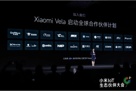
【Lansheng Technology News】Recently, at the 2023 Xiaomi IoT Ecological Partner Conference, NXP Semiconductors was invited to attend as an important partner of Xiaomi and demonstrated the powerful technical resource support provided to the Xiaomi Vela ecological community.
Xiaomi Vela is an embedded IoT software platform built on the open source real-time operating system NuttX and customized for consumer-grade IoT. It can provide a unified software platform on various IoT hardware, shielding the differences in underlying hardware. Through rich components and standardized software frameworks, it provides a unified software interface for upper-level device developers to open up fragmented things. Networked application scenarios greatly reduce the complexity of development and improve development efficiency.
As a global ecological partner of Xiaomi Vela, NXP is deeply involved in the construction of the ecosystem of this development community and has launched a series of technical resources. At this event, NXP highlighted the i.MX RT1060 EVK development kit.
NXP's i.MX RT1060 cross-border MCU is based on the 600MHz Arm Cortex-M7 core and has 1MB on-chip SRAM. It has strong real-time performance and high integration, and is suitable for various industrial and IoT applications. The i.MX RT1060 series provides 2D graphics, camera and various memory interfaces, as well as a wide range of connection interfaces, including UART, SPI, I2C, USB, 2 10/100M Ethernet interfaces and 3 CAN interfaces. Its other features for real-time applications include: high-speed GPIO, CAN-FD, and synchronous parallel NAND/NOR/PSRAM controller.
In addition, i.MX RT1060 has a 2D hardware graphics acceleration PXP module, 3 I2S interfaces for high-performance multi-channel audio, and supports LCD display controller (up to WXGA 1366 x 768). The i.MX RT1060 is available in 225BGA and 196BGA packages, providing greater flexibility with an extended temperature range of -40°C to 125°C.
The i.MX RT1060 series can be developed using NXP's official MCUXpresso tool chain, including SDK, IDE options, and security configuration and configuration tools, enabling rapid development and supporting various real-time operating systems (RTOS) such as FreeRTOS, Xiaomi Vela, Nuttx, Zephyr, etc. .
Xiaomi Vela is fully scalable from micro (8-bit) to mid-range embedded (64-bit) systems with a high degree of standards compliance, easy to port, fully open, highly real-time and powerful. i.MX RT1060 fully supports Xiaomi Vela. Currently supported drivers include ADC, CAN, eLCDIF, ENC, ENET, GPIO, I2S, PWM, SPI, UART and USB. It also supports Vela’s LVGL Demo and can be adapted to Xiaomi The upper component of Vela framework. This combination of soft and hard will provide a powerful technical engine for the development of the Xiaomi Vela ecological community.
Lansheng Technology Limited, which is a spot stock distributor of many well-known brands, we have price advantage of the first-hand spot channel, and have technical supports.
Our main brands: STMicroelectronics, Toshiba, Microchip, Vishay, Marvell, ON Semiconductor, AOS, DIODES, Murata, Samsung, Hyundai/Hynix, Xilinx, Micron, Infinone, Texas Instruments, ADI, Maxim Integrated, NXP, etc
To learn more about our products, services, and capabilities, please visit our website at http://www.lanshengic.com
0 notes
Text
The Future of AI is Here: Cerebras' WSE-2 is the largest computer chip ever built and the fastest AI processor on Earth
See on Scoop.it - Design, Science and Technology
Cluster-Scale Performance on a Single Large-Wafer Chip
Video is here
Programming a cluster to scale deep learning is painful. It typically requires dozens to hundreds of engineering hours and remains a practical barrier for many to realize the value of large-scale AI for their work. On a traditional GPU cluster, ML researchers – typically using a special version of their ML framework – must figure out how to distribute their model while still achieving some fraction of their convergence and performance target. They must navigate the complex hierarchy of individual processors’ memory capacity, bandwidth, interconnect topology, and synchronization; all while performing a myriad of hyper-parameter and tuning experiments along the way. What’s worse is that the resultant implementation is brittle to change, and this time only delays overall time to solution. With the WSE, there is no bottleneck. We give you a cluster-scale AI compute resource with the programming ease of a single desktop machine using stock TensorFlow or PyTorch. Spend your time in AI discovery, not cluster engineering.
Learn more
Designed for AI
Each core on the WSE is independently programmable and optimized for the tensor-based, sparse linear algebra operations that underpin neural network training and inference for deep learning, enabling it to deliver maximum performance, efficiency, and flexibility. The WSE-2 packs 850,000 of these cores onto a single processor. With that, and any data scientist can run state-of-the-art AI models and explore innovative algorithmic techniques at record speed and scale, without ever touching distributed scaling complexities.
1000x Memory Capacity and Bandwidth
Unlike traditional devices, in which the working cache memory is tiny, the WSE-2 takes 40GB of super-fast on-chip SRAM and spreads it evenly across the entire surface of the chip. This gives every core single-clock-cycle access to fast memory at extremely high bandwidth – 20 PB/s. This is 1,000x more capacity and 9,800x greater bandwidth than the leading GPU. This means no trade-off is required. You can run large, state-of-the art models and real-world datasets entirely on a single chip. Minimize wall clock training time and achieve real-time inference within latency budgets, even for large models and datasets.
220Pb/s
High Bandwidth - Low Latency
Deep learning requires massive communication bandwidth between the layers of a neural network. The WSE uses an innovative high bandwidth, low latency communication fabric that connects processing elements on the wafer at tremendous speed and power efficiency. Dataflow traffic patterns between cores and across the wafer are fully configurable in software. The WSE-2 on-wafer interconnect eliminates the communication slowdown and inefficiencies of connecting hundreds of small devices via wires and cables. It delivers an incredible 220 Pb/s processor-processor interconnect bandwidth. That’s more than 45,000x the bandwidth delivered between graphics processors.
Read the full article at: www.cerebras.net
0 notes
Text
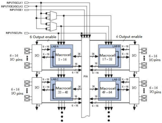
Complex Programmable Logic Devices (CPLDs) are digital integrated circuits with programmable logic cells and interconnections used to implement a variety of digital logic functions for a wide range of applications, including system control, signal processing, and interface management.
Composition of Complex Programmable Logic device(CPLD)
Logic Cells or Macrocells: CPLDs consist of an array of logic cells or macrocells. Each logic cell is a configurable unit that can perform various logic functions, such as AND, OR, XOR, and NOT. It also typically includes a flip-flop for sequential logic operations. The logic cells are the primary building blocks for creating custom logic circuits.
Programmable Interconnects: CPLDs have a matrix of programmable interconnects that allow you to route signals between the logic cells and other components within the device. These interconnects are critical for creating the desired connections between logic cells to implement the desired logic functions.
Input/Output Blocks (IOBs): IOBs are responsible for interfacing the CPLD with external devices. They provide input and output pins that can be connected to external components or other parts of the digital system. IOBs often include features like voltage level translation, pull-up/pull-down resistors, and bidirectional capabilities.
Fixed Function Blocks (Optional): Some CPLDs include fixed function blocks that provide specialized functionality. These blocks may include clock management resources, memory elements (e.g., flip-flops), and counters. The availability of these blocks can vary depending on the specific CPLD model.
Configuration Memory: CPLDs require a configuration memory that stores the logic configuration for the device. This memory holds the information needed to define the behavior of the logic cells and interconnects. Common configuration memory types include Flash memory, SRAM (Static Random-Access Memory), or anti-fuse technology.
Clock Distribution Network: CPLDs often include a clock distribution network that allows for the distribution of clock signals to various parts of the device. This network ensures that all parts of the CPLD are synchronized to the same clock signal when necessary.
JTAG Interface: Many CPLDs feature a JTAG (Joint Test Action Group) interface, which allows for device programming, debugging, and testing. The JTAG interface is commonly used during the configuration process.
Power Supply Pins: Like any electronic component, CPLDs require power to operate. They have power supply pins for providing the necessary voltage levels to the device. These pins may include VCC (positive supply voltage) and GND (ground) connections.
Read more: What is Complex Programmable Logic Device(CPLD)
0 notes
Photo

#Memory Components#Memory Integrated Circuits#Memory Storage Products#Solid State Drives#DRAM Module#DDR#Asynchronous Low Power SRAM#Synchronous SRAM#NAND Flash#SLC NAND Flash#SPI NAND Flash#Managed NAND#Nor Flash#SPI Nor#EEProms#eMMC and eMCP#Excess Inventory Management Services#Obsolescence Management Services#Alliance Memory
0 notes
Text
https://www.futureelectronics.com/p/semiconductors--memory--RAM--static-ram--asynchronous/cy62148ell-55sxit-infineon-7570237
Memory ICs, Random Access Memory, Fast asynchronous SRAM, low power SRAM
CY62148E Series 4 Mbit (512 K x 8) 5.5 - 5.5 V 55 ns Static RAM-SOIC-32
#Infineon#CY62148ELL-55SXIT#RAM#Static RAM#Asynchronous SRAM#Memory ICs#Fast asynchronous SRAM#low power SRAM#circuits#non volatile memory#What is synchronous SRAM#Sync SRAMs#Static random-access memory#volatile SRAM#non volatile sram#flash memory
1 note
·
View note
Text
Significado de memoria RAM
La memoria RAM es la memoria principal de un dispositivo donde se almacena programas y datos informativos. Las siglas RAM significan “Random Access Memory” traducido al español es “Memoria de Acceso Aleatorio”.
La memoria RAM es conocida como memoria volátil lo cual quiere decir quelos datos no se guardan de manera permanente, es por ello, que cuando deja de existir una fuente de energía en el dispositivo la información se pierde. Asimismo, la memoria RAM puede ser reescrita y leída constantemente.
Los módulos de RAM, conocidos como memoria RAM son integrantes del hardware que contiene circuitos integrados que se unen al circuito impreso, estos módulos se instalan en la tarjeta madre de un ordenador. Las memorias RAM forman parte de ordenadores, consolas de videojuegos, teléfonos móviles, tablets, entre otros aparatos electrónicos.
Existen 2 tipos básicos de memoria RAM; RAM dinámica (DRAM) y RAM estática (SRAM), ambas utilizan diferentes tecnologías para almacenar los datos. La RAM dinámica (DRAM) necesita ser refrescada 100 de veces por segundos, mientras que la RAM estática (SRAM) no necesita ser refrescada tan frecuentemente lo que la hace más rápida pero también más cara que la memoria RAM dinámica.
En contrapartida de la memoria RAM existe la memoria ROM es una memoria no volátil ya que la información contenida en ella no es borrable al apagar el ordenador ni con el corte de la energía eléctrica. Para más información puede ver nuestro artículo de memoria ROM.
Tipos de memoria RAM
DDR conocida como SDRAM (Synchronous Dram) es un tipo de memoria RAM, dinámica que es casi un 20% más rápida que la RAM EDO. Esta memoria entrelaza dos o más matrices de memoria interna de manera que mientras se accede a una matriz, la próxima se está preparando para acceder, dicha memoria permite leer y escribir datos a 2 veces la velocidad buz.
DDR2 son unas mejoras de la memoria DDR que permite que los búferes de entrada – salida funcionan al doble de la frecuencia del núcleo, permitiendo que durante cada ciclo de reloj se realizan 4 transferencias. Una memoria DDR a 200 MHZ reales entregaba 400 MHZ nominales, la DDR2 con esos mismos 200 MHZ entrega 800 MHZ NOMINALES.
DDR3 puede ser 2 veces más rápida que la memoria DRR2, la DDR3 teóricamente podía transferir datos a una tasa de reloj efectiva de 800-2600 MHZ, comparado con el rango de DDR2 de 400-1200MHZ o 200-533MHZ del DDR2.
Memoria caché o RAM caché un caché es un sistema especial de almacenamiento de alta velocidad, puede ser tanto un área de reservada de la memoria principal como un dispositivo de almacenamiento de alta velocidad independiente. Una memoria caché es una parte de memoria RAM estática de alta velocidad (SRAM) más que la lenta y barata RAM dinámica (DRAM) usada como memoria principal. La memoria caché es efectiva debido a que los programas acceden una y otra vez a los mismos datos e instrucciones.

1 note
·
View note
Text
#“static random-access memory (sram) market”#“static random-access memory (sram) market overview”#“static random-access memory (sram) research report”#“static random-access memory (sram)”
0 notes
Text
Samsung Semiconductor shares storage solutions in the era of artificial intelligence and big data at ODCC2023

【Lansheng Technology News】On September 13, the "2023 Open Data Center Summit" hosted by the Open Data Center Committee was held at the Beijing International Convention Center. Cui Zhangshi, vice president of Samsung Electronics and head of the memory new business planning department, delivered a keynote speech on "Artificial Intelligence, Machine Learning and Storage Solutions in the Data Era" at the meeting. At the same time, at the booth, Samsung Semiconductor showed participants storage products adapted to the big data era of artificial intelligence and machine learning.
Samsung donated the permanent use rights of the SITS system to ODCC. SITS is a software designed specifically for SSD testing and evaluation. It can help users test the performance and stability of solid-state drives more conveniently and efficiently, and can provide detailed test reports.
At Samsung's keynote speech this time, Samsung Electronics Vice President Choi Chang-seok introduced the "Turing Test" to raise the question of whether machines have the ability to think. He pointed out that one of the important reasons why machines are increasingly capable of "thinking" is memory capacity. . Especially in the fields of artificial intelligence and machine learning, higher memory capacity means better performance.
At the same time, he proposed that since memory capacity is limited by the central processor, we must make full use of storage expander technology and fine-tune tiered solutions to move towards a memory-centric heterogeneous architecture.
He also introduced Samsung’s series of storage products for artificial intelligence and machine learning. High-bandwidth storage "HBM3E" optimized for high-performance computing; 32Gb DDR5 DRAM (fifth-generation double data rate synchronous dynamic random access memory) planned to be available by the end of the year; and Samsung's first 8-channel NAND ultra-high-performance PCIe 5.0 data Central dedicated solid state drive - PM9D3a. The large-scale storage solutions that Samsung will provide in the future include LLC DRAM solutions capable of handling large-scale SRAM workloads, CXL-based storage expanders, and CXL-based memory-semantic SSDs. Samsung continues to develop the gigabit-class ultra-high-capacity storage solution "PBSSD".
Lansheng Technology Limited, which is a spot stock distributor of many well-known brands, we have price advantage of the first-hand spot channel, and have technical supports.
Our main brands: STMicroelectronics, Toshiba, Microchip, Vishay, Marvell, ON Semiconductor, AOS, DIODES, Murata, Samsung, Hyundai/Hynix, Xilinx, Micron, Infinone, Texas Instruments, ADI, Maxim Integrated, NXP, etc
To learn more about our products, services, and capabilities, please visit our website at http://www.lanshengic.com
0 notes
Link
0 notes
Link
#Memory Components#Memory Integrated Circuits#Memory Storage Products#Solid State Drives#DRAM Module#DDR#Asynchronous Low Power SRAM#Synchronous SRAM#Asynchronous Fast SRAM#NAND Flash#SLC NAND Flash#SPI NAND Flash#Managed NAND#NOR Flash#SPI Nor#EEProms#eMMC and eMCP#Excess Inventory Management Services#Obsolescence Management Services#Alliance Memory
0 notes
Text
How different are present-day RAM devices from a regular hard drive?
Modern-day RAM devices are extremely costly considering the integrated circuit system it uses for compiling information. To simply put it, the cost of per unit storage with RAM is higher than other handy devices like hard drives. But the speedier access to data with RAM makes them worth it even with such pricey tags. Any computer manufacturing firm would use a specific amount of RAM in its computer for speedy access and along with it inserts a larger amount of nonrandom permanent storage devices like a hard disk drive. So, check out your laptop specification and you will observe that it includes between 2-8 GB of RAM. But more than a hundred GB of hard disk storage capacity is maintained in an average computer system.
Types of Random Access Memory (RAM)
Primarily you will find two types of Random Access Memory and those are Static RAM aka SRAM and Dynamic RAM or DRAM. Let’s move into them one by one –
Dynamic RAM (DRAM)
DRAM is the type of RAM mainly used for computers’ core memory. DRAM memory cell is composed of three main units and those are:
a capacitor built within the integrated circuit.
A transistor and
Within the capacitor, you will find the stored data bit.
The electric capacitor tends to leak and either has a charged or empty DRAM cell without any charges. Therefore, every few milliseconds, DRAM frequently refreshes the electronic charges to sustain the leaks of the capacitor. Ultimately, the transistor acts as a gate and decides if the value of the capacitor is readable or not. So, these types of RAM are volatile and should be refreshed frequently with the help of voltage, or else the information stored in it will get removed.
Static RAM (SRAM)
Unlike DRAM which has a capacitor for each of its cells, the Static RAM works with multiple transistors precisely 4 to 6 for every memory cell. Essentially SRAM is used for cache. The longevity of the data stored in SRAM is directly dependent on how long the power is supplied to the computer system. It does not have the capability like DRAM to refresh regularly for sustaining data. The added advantage of SRAM is its fast speed which makes it more costly in the market as compared to DRAM.
DRAM vs SRAM: a tabular comparison
So, before proceeding further, let’s have a tabular comparison of both DRAM and SRAM in terms of their available features-
Dynamic RAM (DRAM)
Static RAM (SRAM)
Due to its higher accessing time, it’s slower than SRAM.
SRAM can access data at a faster pace.
Less costly as compared to SRAM.
Expensive than DRAM.
Since the information is stored in its capacitor therefore it can work with a reduced power supply.
To retain information SRAM would require a constant supply of power.
It comprises a small internal integrated circuit system along with its one-bit memory cell.
It consists of a complex internal circuit system.
With DRAM you can expect a larger storage capacity.
Following the above point, it has a lesser storage capacity than the DRAM physical memory chip.
Higher packaging density.
Low packaging density.
Therefore, among the two types of RAM, it’s the DRAM, used as the most reliable and pocket-friendly volatile memory for any computer system.
Other types of DRAM
As you already have noted, DRAM is one of the two types of RAM. So, now you may find that within the category of DRAM there are some varieties. Let’s have a look at them.
1. Synchronous DRAM (SDRAM)
SDRAM is different from any of the traditional built DRAM because it’s a semiconductor memory that enables it to run faster for any computing technology. The SDRAM external pin interface works in coordination with the CPU clock signals. Therefore, the SDRAM chips only get ready to operate when the CPU enables them. The seed of data transfer in a normal SDRAM takes place up to 132 -134 MHz.
2. Rambus Dram (RDRAM)
The name of the Rambus DRAM is after its manufacturing company called Rambus, working in the market since the late 1990s. The composition of RDRAM includes a RAM, a bus path linking RAM to microprocessors and computer systems, and a RAM controller. The following subcategory of RAM is used to store info for any graphic cards or video game devices. A typical RDRAM takes 1 GHz speeds in data transferring.
3. Double Data Rate SDRAM (DDR SDRAM)
To put it simply DDR SDRAM is a type of volatile memory that has the capacity of double the bandwidth of a single data rate Synchronous DRAM. They do so by maintaining the same clock frequency with a method called double pumping. When you apply the double pumping method then your data would get transferred by falling and rising the edges of the clock signals. However, the clock signal frequency stays unchanged.
With time the DDR SDRAM model was followed by DDR2 SDRAM then DDR3 SDRAM and now we have the DDR4 SDRAM generation. All of these models follow the double pumping means for the data transfer. And each succeeding generation, the performance of the data transfer gets faster. Any new RAM stick in the market usually installs DDR4 chips for your computer.
4. Asynchronous DRAM. (ADRAM)
With an ADRAM the memory device timing is kept under check based on a specialized memory controller circuit. This memory circuit sends the required control signals for time control. And as a result, the CPU usually takes note of the delay while responding to the memory.
5. Cache DRAM (CDRAM)
CDRAM is a mixed type of DRAM memory that works with an on-chip cache SRAM memory. The cache memory makes it a high-speed buffer for the functioning of the main DRAM. Initially developed by Mitsubishi a typical CDRAM comprises a smaller SRAM cache.
How much RAM do you need?
The amount of RAM you should look for depends on how dependent you are on your computer. For those who use their computer only for minor document editing, working on spreadsheets, or internet browsing, a computer of up to 8 GB RAM would suffice. But for Gamers who are daily running heavy memory programs then they at least would need 16 GB RAM for operating their computer smoothly.
Checking your RAM is also easy. For Windows: go to the start menu > system information > tap on the result for opening it. From there find the installed Physical memory (RAM) section.
Comparing RAM, ROM, and General storage.
RAM, as you know, is the computer’s short-term memory storage, unlike general memory where information is stored in massive quantities. Unlike them, ROM or Read Only Memory consists of some unique information for turning the computer on. From is situated at the motherboard of your computer and instructs your computer how to function. When you first turn your computer on, then the first thing your computer does is access the ROM. Without the ROM, you won’t be able to own anything else.
As you know how RAM works, therefore you know RAM data is constantly changing. Unlike the RAM of your computer, you can’t change the ROM and for this reason, it’s called – Read Only. The speed of RAM is generally higher than ROM. Other than that, ROM data is not easily accessible by the CPU unless the same data is stored in RAM.
RAM also differs from nonvolatile SSDs or System Storage Data as the latter type of data doesn’t get lost when power loses. Every time you save a file then you are copying the inputted data from your RAM to the hard disk drive so that it doesn’t get lost.
RAM: Where is the future directing us!
Now that you are clear about what is Random Access Memory, how RAM works, and its types, let’s end by looking at the broader picture. With the accessibility of ReRAM (Resistive RAM) technologies, we can expect a nonvolatile storage system that would be based on an even higher switching speed than any other nonvolatile storage. At present, 3D X Point techs like Intel Optane are constantly working to bridge the gap between any DRAM and NAND flash memory. So, with time we can expect the advancement of technologies will erase any distance between RAM and storage systems.

0 notes