#vlsidesign
Explore tagged Tumblr posts
Visit Tumblr Blog
Explore Tumblr blogs with no restrictions, modern design and the best experience.
Last Seen Tumblr Blogs


Fun Fact
In Q3 of 2020, 31% of US users access the Tumblr app daily.
Text
AI in Semiconductor Manufacturing: Powering the Next Generation of Innovation

The semiconductor industry is undergoing a radical transformation, and at the forefront of this change is Artificial Intelligence (AI). As chips become smaller, faster, and more complex, manufacturers are turning to AI to overcome longstanding production challenges — from yield improvement to real-time process optimization.
AI is no longer a futuristic concept; it’s a strategic enabler that is reshaping how semiconductors are designed, manufactured, and optimized. Implementing AI-driven automation requires expert guidance. Orbit & Skyline's Equipment Engineering and Process Engineering services ensure that semiconductor fabs utilize the latest Engineering.
Transforming Process Optimization
Modern semiconductor fabs generate an enormous volume of data from tools, sensors, and production systems. Traditional methods struggle to process this data fast enough to provide actionable insights. This is where AI excels.
By leveraging machine learning algorithms and data-driven models, AI can analyze real-time data streams and predict outcomes with high accuracy. Manufacturers can now detect deviations early, adjust parameters dynamically, and reduce defects before they become costly.
According to industry studies, AI implementation in chip fabrication can improve process efficiency by up to 30%, contributing to lower costs, faster time-to-market, and higher yields.
Autonomous Fabs: The Future of Manufacturing
Looking ahead, the concept of autonomous fabs is gaining momentum. These are AI-powered, self-optimizing factories capable of managing the entire semiconductor production lifecycle — from material input to final inspection — with minimal human intervention.
Autonomous fabs continuously monitor operational data, learn from outcomes, and adapt processes in real-time. This not only increases precision and consistency but also minimizes downtime and waste.
Building Smarter Ecosystems with AI and IoT
The adoption of AI in semiconductor manufacturing is closely linked to the rise of connected ecosystems. Integrating AI with IoT platforms and Manufacturing Execution Systems (MES) allows for seamless data exchange across all stages of production.
Key benefits include:
End-to-End Connectivity: Ensures complete visibility from design to delivery.
Predictive Maintenance: AI predicts tool failures before they happen, reducing unplanned downtime.
Real-Time Analytics: Enables faster decisions and on-the-fly process corrections.
Enhanced Resource Allocation: Improves utilization of materials, tools, and energy.
Together, these technologies create a more agile, intelligent, and scalable manufacturing environment.
Challenges on the Road to AI-Driven Manufacturing
Despite its promise, implementing AI at scale in semiconductor manufacturing is not without hurdles:
Data Quality & Availability: AI systems require large volumes of high-quality, labeled data — often hard to collect in cleanroom environments.
Legacy System Integration: Many fabs still run on legacy infrastructure, making integration complex and time-consuming.
Model Explainability: For AI to gain acceptance on the shop floor, engineers need transparency into how decisions are made. Black-box models can create trust issues.
Overcoming these challenges requires strong collaboration between AI solution providers, semiconductor OEMs, and equipment manufacturers.
The Road Ahead: AI + Emerging Tech
The next frontier involves combining AI with emerging technologies like Edge AI and Quantum Computing. Edge AI enables real-time inference and decision-making directly on the production floor, reducing latency and bandwidth demands. Meanwhile, quantum computing offers the potential to accelerate simulations and model complex chemical processes with unmatched speed.
These advancements will unlock new efficiencies and push the boundaries of what’s possible in chip design and manufacturing.
Partnering for Progress With 15+ years of expertise and a global team of 500+ engineers, Orbit & Skyline is a trusted partner in the semiconductor industry. If you are looking for a semiconductor services and solution partner, reach out to us at [email protected]
0 notes
Text

Join the Best VLSI Course in Tirupati – Upgrade Your Career in Chip Design
A valid opportunity for anyone wanting to build a career in the semiconductor industry. Come, enrol in the best VLSI course up for grabs in Tirupati, for students and professionals striving to become experts in VLSI Design, Verification, and FPGA Implementation. The program teaches Digital Design, Verilog HDL, ASIC, VHDL, and many more relevant topics for making you fit for a job in leading tech companies.
We provide basic internship, real-time projects, and professional mentoring at the core of Tirupati for practical exposure. Designed for CSE, ECE, or EEE students, this course is tuned to give you a competitive edge in the fast-growing VLSI industry.
Students are guided at a project level in VLSI by Takeoffupskill, which best suits students in their last year of B.Tech or M.Tech. We are the very first in Tirupati to be an overall analytical and lab-on type ground for training VLSI.
#VLSICourse#VLSITraining#VLSIDesign#VLSIEngineering#ASICDesign#FPGAProgramming#ChipDesign#SemiconductorTraining#DigitalElectronics#HardwareDesign#TakeoffEduGroup#takeoffupskill
0 notes
Text
Smarter VLSI Design Through AI-Powered Innovation
As semiconductor technology continues to evolve, the demand for high-performance and energy-efficient chips is reshaping how integrated circuits are designed. Traditional VLSI (Very-Large-Scale Integration) methods, while foundational, are becoming insufficient for the scale and complexity of modern electronics. To bridge this gap, Artificial Intelligence (AI) is being integrated into VLSI design workflows — unlocking smarter, faster, and more optimized chip development.
Tech4BizSolutions is actively leveraging AI to enhance every stage of the VLSI lifecycle, from architecture planning to post-silicon validation.

What Is AI-Driven VLSI Design?
AI-driven VLSI design refers to the application of machine learning, deep learning, and data analytics to automate and optimize various stages of chip design and manufacturing. Unlike conventional design flows, AI can identify patterns, predict outcomes, and generate insights from massive datasets in real-time.
Key advantages include:
Improved performance-to-power ratio
Reduced manual effort in layout planning
Faster design rule checking and validation
Enhanced yield prediction and fault analysis
Tech4BizSolutions integrates AI across multiple design layers, reducing time-to-market while improving design accuracy and production reliability.
How Tech4BizSolutions Enhances VLSI with AI
At Tech4BizSolutions, we fuse our deep domain knowledge in semiconductor design with cutting-edge AI techniques. Here’s a breakdown of how we apply AI to make VLSI smarter:
1. AI in Design Space Exploration
Design space exploration is one of the most time-consuming phases of VLSI. Our AI models intelligently evaluate thousands of possible configurations, identifying the most efficient architecture with minimal resource usage.
Tech4BizSolutions Result: Up to 50% reduction in time spent exploring design alternatives.
2. Automated Floorplanning and Layout Optimization
Floorplanning and placement affect timing, area, and power consumption. We use neural networks to predict optimal component placement and signal routing paths, reducing congestion and delay.
Tech4BizSolutions Advantage: Increased chip efficiency with reduced layout iterations.
3. AI-Enhanced Timing and Power Analysis
Tech4BizSolutions uses AI models trained on historical data to predict timing violations and power bottlenecks before physical implementation. This allows early-stage corrections, saving time and silicon costs.
Outcome: More accurate PPA (Performance, Power, Area) metrics at the RTL level.
4. Fault Detection and Yield Improvement
AI helps detect subtle, non-obvious design flaws by recognizing patterns in simulation and test bench outputs. We also use AI to simulate rare corner cases that are typically missed in standard verification cycles.
Business Impact: Higher first-pass silicon success rates and lower manufacturing risks.
5. Adaptive Learning Systems for Continuous Optimization
Our AI systems are not static. They learn and evolve with every project. We build feedback loops where post-silicon data refines future simulations and models — creating a smarter design pipeline over time.
Long-term Benefit: Each new chip design becomes more efficient than the last, reducing NRE (Non-Recurring Engineering) costs.
Tech4BizSolutions: Delivering Tangible Business Value
By embedding AI into VLSI design workflows, Tech4BizSolutions helps clients:
Speed up development cycles by up to 40%
Reduce power consumption by designing for energy-aware applications
Increase IC performance through AI-informed microarchitecture tuning
Minimize silicon iterations and time spent on debugging
Predict and eliminate faults before tape-out
This makes our approach ideal for industries like:
Consumer Electronics
Automotive & EV
Industrial Automation
Telecom and 5G
IoT and Edge Devices
Real-World Use Case
Let’s say a client needs a custom AI accelerator chip for real-time video processing. With traditional VLSI design, modeling workloads, optimizing for latency, and reducing power draw can take months.
With Tech4BizSolutions’ AI-enhanced VLSI flow, we:
Use AI models to simulate expected video processing loads
Automatically adjust component placement for thermal efficiency
Predict the power envelope across real-world scenarios
Validate logic paths using AI-driven test vectors
Result: A custom ASIC delivered 30% faster with optimized performance and reliability.
Conclusion: The Future of Smarter Chip Design Starts Here
VLSI design is undergoing a significant transformation. As chip complexity continues to rise, integrating AI into every stage of the design and manufacturing process is not just an option — it’s a necessity.
Tech4BizSolutions is proud to lead this evolution with intelligent VLSI design solutions that are adaptive, efficient, and future-ready. Our AI-infused approach ensures not only faster development but smarter chips that can meet the demands of modern, connected, and data-driven applications.
Whether you’re building the next-gen smart device or need custom silicon for industrial systems, Tech4BizSolutions has the tools, talent, and technology to deliver.
Want to learn how AI can power your next chip design?
Contact Tech4BizSolutions today and explore the possibilities of intelligent VLSI.
#VLSIDesign#AIDrivenDesign#SemiconductorInnovation#ChipDesign#Tech4BizSolutions#HardwareInnovation#ASICDesign#EDAtools#DesignAutomation#TechSolutions#PowerEfficientDesign#CustomChipDesign
0 notes
Text
VLSI Projects Using Xilinx Software
Very Large Scale Integration VLSI Xilinx software projects entail the construction of circuits that have millions of transistors on a single chip. Xilinx offers encompassing FPGA solutions like Vivado and ISE for VLSI design where end-user can implement his/her digital system with utmost ease at high level of abstraction. Common offerings are usually of the form of ASICs that incorporate digital systems such as processors, memory interfaces, communication interfaces, or specific Circuits. One of the most selected project ideas is to develop an MIPS microprocessor on Xilinx FPGAs for ALU, control units, registers and the like. Another frequently assigned project is the synthesis of the digital signal processing (DSP) system associated with pulsing or graphic processing. Its software includes a programmable logic device programming software, FPGA development software, an integrated circuit/multi-chip module fabrication software, simulation software as well as a hardware verification and timing analysis software that helps confirms that the VLSI design is functional and efficient. These projects are useful in grasping concepts like digital logic, HDL, and the usage of FPGAs to conceptualize electronic systems.
#vlsi#xilinx#software#projects#fpgasoultion#digitalsystem#VLSIdesign#engineeringprojects#takeoffedugroup
0 notes
Text
Seminaar on From Campus to Corporate in VLSI Design- At DCE

On August 23, 2024, the ECE Department of Dronacharya College of Engineering hosted an insightful seminar on "Campus to Corporate in VLSI Design," connecting our students directly to the booming semiconductor industry. Led by Mr. Rajat Kumar Singh, Founder & CEO of VLSI For All Pvt. Ltd., the seminar provided an in-depth exploration of the VLSI (Very Large Scale Integration) design process and its critical role in the semiconductor industry. Mr. Singh, a leading expert in the field, shared his wealth of knowledge and industry insights, guiding our students on how to successfully transition from academic learning to professional excellence in VLSI design. This seminar is a testament to our commitment to equipping students with the latest industry trends and skills, ensuring they are well-prepared to enter the workforce and make a significant impact in the ever-evolving semiconductor industry. We thank Mr. Rajat Kumar Singh for his invaluable contributions and for inspiring the next generation of engineers!
#VLSIDesign#SemiconductorIndustry#CampusToCorporate#EngineeringExcellence#DronacharyaCollege#ECE#IndustryInsights#FutureEngineers#TechLeadership#InnovativeLearning#VLSIForAll
0 notes
Text
Power-Aware Recursive Squarer Architecture
In modern digital systems, arithmetic operations such as squaring, addition, multiplication, and division form the foundation of computation. However, implementing these operations with full precision can lead to excessive power consumption, increased area, and longer delay—factors that are especially problematic for resource-constrained systems such as portable or embedded devices. To address these challenges, this work presents a novel approach using approximate computing to design low-power, area-efficient squaring circuits, which are vital in numerous applications such as signal processing, image processing, and machine learning.
#sciencefather#researchfather#phenomeno#ApproximateComputing#DigitalCircuits#LowPowerDesign#VLSIDesign#HardwareOptimization
International Phenomenological Research Awards Website Link: https://phenomenologicalresearch.com/ Nomination Link: https://phenomenologicalresearch.com/award-nomination/?ecategory=Awards&rcategory=Awardee Contact Us For Enquiry: [email protected]
#phenomenology#researchawards#internationalawards#academicrecognition#qualitativeresearch#phenomenologicalstudies#scholarlyachievement#researchexcellence#humanscienceresearch#professor#academic#sciencefather#voicetherapy#mentaleffort#patientperception#vocalrehabilitation#speechtherapy#cognitiveload#patientexperience#therapeuticoutcomes#voicehealth#healthcarepsychology
Youtube:https://www.youtube.com/channel/UCga5JVq6VElDLksyLzNqybg Twitter: https://x.com/compose/post Instagram: https://www.instagram.com/phenomenoresearch/?hl=en Facebook: https://m.facebook.com/phenomeno002/ Pinterest: https://in.pinterest.com/phenomenoresearch/ Blogger: https://phenomenological21.blogspot.com/ Whatsapp Channel: https://whatsapp.com/channel/0029Vazl6GD7z4kkTlmIbc29
0 notes
Text
DEPARTMENT OF ELECTRONICS & COMMUNICATION ENGINEERING
ADMISSIONS ARE OPEN 2023-24! Welcome to Mewar University, Chittorgarh, (Raj.)
Enrollment is now ongoing, Join India’s best University with a 100% Scholarship. 🎓
👉 Programs Offered
↪️ M.Tech in Electronics & Communication Engineering
↪️ M.Tech Digital Communication VLSI Design
↪️ Ph.D. Electronics & Communication Engineering
👉 Electronics Engineering Labs
↪️ Software Lab
↪️ Communication Lab
↪️ Satellite Communication Lab
↪️ Internet of Thing Lab
↪️ Microwave Engineering Lab
↪️ Digital & Microprocessor Lab
↪️ PCB Design Lab
↪️ Junkyard War
↪️ Science Fair
↪️ Workshop
👉 Key Features
✅ Basics and Advanced
✅ Experienced Professional Faculties
✅ Practical Learning Experiences
✅ World Class Infrastructure & Top faculties
✅ 100% Internship and 100% Placement opportunities.
🚀Top Recruiters
🔍Wipro, 🔍Indian Railways, 🔍BSNL, 🔍Sail, 🔍Jk Cement, 🔍Axis Bank, 🔍ICICI Bank, etc.
Stay Tuned for more updates!
For Registration Visit:
🌐www.mewaruniversity.org
Contact Details:
☎️180030707373, 7014136252, 9414497990
#AdmissionsOpen #Electronics #DigitalCommunication #VLSIDesign #SoftwareEngineer #Scholarship #MicrowaveEngineering #KnowledgeToWisdom #MewarUniversity #TopUniversityInRajasthann #BTech #EducationForSuccess #BestEngineringCollege #Cuet #BestUniversityInRajasthan #AdmissionsOpen2023 #BTechAdmissions #UGCourses #MasterDegree #UnderGradCourses #Engineering #PhD #BachelorDegrees
0 notes
Text
VLSI DESIGN BASICS
Physical design
In integrated circuit design, physical design is a step in the standard design cycle which follows after the circuit design. At this step, circuit representations of the components (devices and interconnects) of the design are converted into geometric representations of shapes which, when manufactured in the corresponding layers of materials, will ensure the required functioning of the components. This geometric representation is called integrated circuit layout. This step is usually split into several sub-steps, which include both design and verification and validation of the layout.
Modern day Integrated Circuit (IC) design is split up into Front-end design using HDLs, Verification, and Back-end Design or Physical Design. The next step after Physical Design is the Manufacturing process or Fabrication Process that is done in the Wafer Fabrication Houses. Fab-houses fabricate designs onto silicon dies which are then packaged into ICs.
Each of the phases mentioned above has design flows associated with them. These design flows lay down the process and guide-lines/framework for that phase. Physical design flow uses the technology libraries that are provided by the fabrication houses. These technology files provide information regarding the type of silicon wafer used, the standard-cells used, the layout rules (like DRC in VLSI), etc.
2 notes
·
View notes
Photo

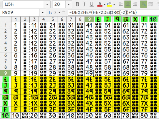

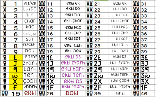
zn se zinc , zr se zirconium but no j q in mendeelev periodic table in chemistry.
so z vill be in zemistry810 for more precision zemistry for medicines & other fields.
&
so let us move f j q x w phrom zinglish/zemistry to maths810 Az :
1_vn 2_tu 3_Three 4_phor 5_phaiv 6_siks 7_seven 8_et 9_nine L_ten J_zilevn Q_kvAlv W_dblu X_Aksen F_phen 10_vnti 2 Thumbs phur biometric sign , shou , svitch 8 phingers to type & count as :
8+8 = 10 = vnti = 4*4
https://github.com/zava810/mintos/blob/main/maths810.md
#mathematics#vlsidesign#verilog#vhdl#flutterdev#edu#education#elearning#onlinetutorindelhi#primary school#student#teaching
0 notes
Link
This technology is using to design or create an IC which takes lower space and is also very efficient by using more than a thousand transistors in combination called as VLSI. VLSI design is the process in which making or creating an integrated circuit is developed by the combinations of thousands of tiny microscopic transistors infused in a single chip. Generally, a VLSI chip designer is the one who designs the functions of the system on a chip called as SOC as per the requirements.
Why VLSI projects are Important?
Large circuits are out-dated and those who are still using them continuously face a lot of problems. However, VLSI solves this issue by decreasing the size of the circuit. It also helps in reducing the price of a computer system. VLSI chip increases the speed of the operating system. The computer utilizes less power which is beneficial for any user. VLSI technology is very much reliable. Finally, everything being in a tiny circuit helps in saving a lot of space.
The latest trending technologies such as high resolution and low bit-rate video and mobile phone communications are possible because of VLSI. This gives the end-users a large amount of applications, processing power and also portability. This trend is expected to grow in the upcoming years. Therefore, if you are thinking about a career in this field, doing VLSI Projects is the best idea.
Start your career with a good project
Pantech eLearning Chennai is an Online Learning Service provider. We are providing some of the best VLSI Projects.
Given below is the list of Top Projects we are providing:
RoBA Multiplier with MAC Unit
Implementation of Reed-Solomon Encoder
High Performance Wallace Multiplier
A Novel high speed dynamic comparator
High Performance Array Multiplier
Design and implementation of Median Architecture
Design of Linear Feedback Shift Register
A high speed design of 16 bit Vedic Multiplier
VLSI architecture for AES Decryption algorithm
Design of a Dual Port RAM using Verilog
Visit our Website and Book your Projects Now.
0 notes
Text
Best VLSI Projects for Final Year Students
Here are some great VLSI project ideas for final-year students:
1. Image Processing System on FPGA: Algorithm, such as edge detection or image filtering should be performed through the usage of FPGAs for optimal performance.
2. Low-Power SRAM Design: Design and simulate a low-power Static Random Access Memory (SRAM) cell, targetting leakage and dynamic power dissipation.
3. Digital Signal Processor (DSP) Design: Design an example of a DSP that will allow a specific signal to be filtered or, for instance, undergo FFT.
4. Wireless Sensor Network (WSN) Protocol Implementation: Devise a VLSI based sensor node for wireless communication that will support protocols used in data transmission.
5. Reconfigurable Hardware Architecture: It is necessary to elaborate a box which is able to evolve in order to support several applications: in this context, it is possible to try to reconfigure parts of the hardware during the runtime according to the specific needs of the client application.
6. Cryptographic Hardware Accelerator: Propose and design a device for which you could use cryptographic algorithms or primitives including AES or RSA where optimization of both speed optimization and security is important.
7. System-on-Chip (SoC) Design: Selected h/w architects use Verilog or VHDL to design a including microcontroller, memory and other peripherals.
8. Artificial Neural Network (ANN) on FPGA: Devise a mini ANN for image recognition and other related work and optimally use the features of parallel processing provisioned by FPGAs.9. Automated VLSI Testing Tool: Design a testing and validation software system that has reduced time and eliminated errors in conducting tests of VLSI designs (Very Large Scale Integration).
10. Temperature Sensor with Data Logger: It will be a VLSI (Very Large Scale Integration) chip for measuring temperature and recording data, with the capability to display the data on a PC or a mobile connection.
All these project proposals present prospects to learn diverse aspects of VLSI design and implementation in addition to enhancing creativity. Choose one that you are interested in and which you can afford to do!
#vlsi#finalyear#verylargescaleintegration#VLSIDesign#engineeringstudents#studentsprojects#takeoffedugroup#takeoffprojects
0 notes
Text
Power-Aware Recursive Squarer Architecture
In modern digital systems, arithmetic operations such as squaring, addition, multiplication, and division form the foundation of computation. However, implementing these operations with full precision can lead to excessive power consumption, increased area, and longer delay—factors that are especially problematic for resource-constrained systems such as portable or embedded devices. To address these challenges, this work presents a novel approach using approximate computing to design low-power, area-efficient squaring circuits, which are vital in numerous applications such as signal processing, image processing, and machine learning.
#sciencefather#researchfather#phenomeno#ApproximateComputing#DigitalCircuits#LowPowerDesign#VLSIDesign#HardwareOptimization
International Phenomenological Research Awards Website Link: https://phenomenologicalresearch.com/ Nomination Link: https://phenomenologicalresearch.com/award-nomination/?ecategory=Awards&rcategory=Awardee Contact Us For Enquiry: [email protected]
#phenomenology#researchawards#internationalawards#academicrecognition#qualitativeresearch#phenomenologicalstudies#scholarlyachievement#researchexcellence#humanscienceresearch#professor#academic#sciencefather#voicetherapy#mentaleffort#patientperception#vocalrehabilitation#speechtherapy#cognitiveload#patientexperience#therapeuticoutcomes#voicehealth#healthcarepsychology
Youtube:https://www.youtube.com/channel/UCga5JVq6VElDLksyLzNqybg Twitter: https://x.com/compose/post Instagram: https://www.instagram.com/phenomenoresearch/?hl=en Facebook: https://m.facebook.com/phenomeno002/ Pinterest: https://in.pinterest.com/phenomenoresearch/ Blogger: https://phenomenological21.blogspot.com/ Whatsapp Channel: https://whatsapp.com/channel/0029Vazl6GD7z4kkTlmIbc29
0 notes
Photo

Agimus Technologies Private Limited Proud to Present Agimus Pine S7: Xilinx Spartan 7 Kit designed and developed in India..Complete Kit is designed and Developed in #India Agimus Technologies Private Limited Xilinx Xilinx product Agimus Academy Xilinx FPGA Agimus Technologies Private Limited +91 9538757011 [email protected] www.agimustech.com #xilinx #xilinxfpga #fpga #makeinindia #atmanirbharbharat #madeinindia #skillindiamission #Skillindia #fpgadesignengineers #fpgas #fpgadesignengineers #fpgakit #xilinxspartan7 #agimustech #agimuspine #agimuspinefpga # #vhdlcode #engineering #vlsidesign #fpgadevelopment #career #projects (at Agimus Technologies PVT LTD) https://www.instagram.com/p/CKjiL_gnztO/?igshid=2nt6joko0asg
#india#xilinx#xilinxfpga#fpga#makeinindia#atmanirbharbharat#madeinindia#skillindiamission#skillindia#fpgadesignengineers#fpgas#fpgakit#xilinxspartan7#agimustech#agimuspine#agimuspinefpga#vhdlcode#engineering#vlsidesign#fpgadevelopment#career#projects
0 notes
Link
he VLSI online course and offline offered by Cranes is way too student-friendly in all aspects. You will get special study sessions, expert assistance and guidance, study materials, placements for jobs and even lifelong material access to build your future in a much better way
0 notes
Photo
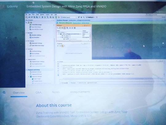
How about finding a good course for FPGA implementation Here is what we want to share for better learning ---------------------------------------------------------------------------------- Like👍 ll comments📝 II Share📢 ➡️Keep Supporting🙏 ---------------------------------------------------------------------------------- . . ---------------------------------------------------------------------------------- Follow (@nationin) for more stuff. ---------------------------------------------------------------------------------- . . _____________________________________________________ #zedboards #fpgalearning #fpgaproject #vlsidesign #nationin #vlsi #electronics #semiconductor #silicon #industry #learn #learning #instalearn #engineers #jobs #job #work #experiment #learn #the #things #fpga #instagram #technology #vlsi #industry #tools #vivado #projects #start #engineers #engineering #life #electronics #engineers #vivado #zedboard #zedboards https://www.instagram.com/p/B9gXbwrn9iG/?igshid=l6lty9zfhd16
#zedboards#fpgalearning#fpgaproject#vlsidesign#nationin#vlsi#electronics#semiconductor#silicon#industry#learn#learning#instalearn#engineers#jobs#job#work#experiment#the#things#fpga#instagram#technology#tools#vivado#projects#start#engineering#life#zedboard
0 notes