#Copper Core PCB
Explore tagged Tumblr posts
Visit Tumblr Blog
Explore Tumblr blogs with no restrictions, modern design and the best experience.
Last Seen Tumblr Blogs


Fun Fact
In February 2021, Tumblr had 518.6 million blog accounts.
Text
Learn the Traits to Find the Best Mcpcb Manufacturer for Your Needs
Metal-core printed circuit boards are one of the most significant spare parts you need to operate and control electronic goods. The quality of this spare will affect the functioning of the entire device. Hence, the manufacturers and the suppliers of the product are some of the elemental stakeholders for electronic device-producing brands. Naturally, due to massive demand, you can find several makers and suppliers in the industry. In this article, we will discuss the traits to discern the best.
Years of experience
The first aspect which you must find out to work with the best mcpcb manufacturer is the number of years for which the company has been operational in the market. You must look for a brand which has been in the market for a minimum of one and a half decades.
Service Array
Services from the top manufacturers and suppliers can help patrons get the best value for their investment. Some of the vital services you can get from the market leaders is mcpcb assembly, mass production, product prototype and innovative designing. These brands are masters in customization and they can change and adapt their products as per the precise customer requirements.
Product Array
Apart from service variety these brands can also act as some of the best single window service providers for different products like single layer metal core pcb, double sided metal core pcb, two layer aluminum base pcb and multilayer aluminum base pcb. Hence irrespective of your requirement specifications you can turn to a single vendor to meet all your business needs.
Quality control certificate
Finally, before you select a vendor for your business one of the main things which you must check is quality assurance certifications for the products from the vendor. This is one of the parameters that give you assurance for the product quality into which you are investing and also for their internal procedures and organization culture. These are the vendors who can add much value to your business.
0 notes
Text
Медный сердечник PCB - медный фундамент + изоляция + медь
PCB с медным сердечником - это PCB с медной базой + изоляцией + слоем медной схемы, также известный как PCB с медной базой, PCB на медной основе и PCB с медной оболочкой.
ПХБ на основе меди - это металлический сердечник с медной пластиной. Если фундамент гибридного PCB представляет собой медную пластину, встроенную в пластину FR4, то это также PCB на основе меди.
#pcb fabrication#pcb assembly#pcb manufacturer#aluminium pcb#pcba manufacturing#pcb#flex pcb#flex circuit pcb#pcb design#led pcb#Copper core pcb
0 notes
Text
Copper core PCB is a copper substrate + Insulated layer + copper
Copper core PCB is a copper substrate + Insulated layer + copper circuits layer PCB,also, it is called copper substrate pcb, copper based pcb,copper clad pcb.
A copper base PCB is a metal core PCB with a copper substrate. If a hybrid PCB whose substrate is a copper plate inlay in the FR4 board, it is also a copper base PCB.
Usually, copper-base PCBs have the same structure as aluminum PCBs - single-layer, double-layer with single component-mounting side, double-layer with dual component-mounting sides, and four-layer with dual component-mounting sides. Even they use the same prepreg material to insulate the copper layers. However, the copper substrate (398W/mK) has better thermal conductivity than the aluminum substrate (237W/mK).
#pcb#pcba#pcb manufacturer#aluminium pcb#ceramic pcb#pcb assembly#heavy copper pcb#mpcb#Metal core pcb#Copper core PCB#fpcb
0 notes
Text

Copper core PCB is a copper substrate + Insulated layer + copper circuits layer PCB,also, it is called copper substrate pcb, copper based pcb, copper clad pcb. https://www.htmpcb.com/metal-core-pcb-c-10.html
PCB PCB Manufacturer PCB Manufacturing Electronics
0 notes
Text
LED PCB Assembly
What is the LED Circuit Board assembly?
Generally, LED PCB assembly is considered to be a circuit board that has the LED components soldered to it. The LED is soldered to the printed circuit board and features a chip that creates the light as electrically connected. A thermal heat sink and a ceramic base are used to bond the chip. Not all the PCB products can be used in Led industry, as an LED PCB is easy to create a high volume of heat, but making it hard to cool with traditional methods. For this reason, metal core PCB is widely used in LED application because of their enhanced ability to dissipate heat, especially aluminum pcb is often used to fabricate PCB for LED lights.
We’ve had great LED PCB assembly experiences with top LED chips to brand such as Cree, Luxeon, Osram, Nichia, Lumileds, MLS, EVERLIGHT, Samsung, LG, Seoul., etc. PCB LED lights can be incorporated into numerous lighting applications due to their combination of excellent energy efficiency, low cost and maximum design flexibility.

Application of LED PCB Assembly
Hitechpcba serves customers in different industries, providing highly reliable and innovative LED PCBs for various applications:
• Horticulture light LED PCB Assembly
• LED controller PCB Assembly
• Computer LED display and indicators
• LED lights PCB Assembly for medical use
• Automotive LED PCBs Assembly include PCBs for brake lights and headlights
• Street lighting LED PCB Assembly
• Flashlights and camping accessories
• Traffic light PCB Assembly
• Commercial lighting LED PCB Assembly
LED PCB Assembly specification
Number of layers for LED PCB
These layers are made up of aluminum and magnesium, but now have Copper base material and Ceramic base materials for LED PCB industry, we can meet it.
Aluminum LED PCBs stand out among other PCBs because it has a good insulation characteristic and has a better machinery performance, the cheap cost is one important factor too.
Types of layers for LED PCB Assembly
Normally, the base layer is made using aluminum alloy metal.
This aluminum alloy substrate used in making the base makes it ideal for through-hole technology which transfers and dissipates heat.
A thermal insulation layer is made using some ceramic polymer which has good viscoelasticity characteristics.
It is highly heat resistant and protects the PCB against heat and mechanical stress.
The circuit layer, which is covered by a copper foil which can range from one to ten ounces.
LED Board type- single or in panel
Some boards are shapeless. For this reason, LED PCB panels are used. This reduces time, labor production and testing time.
Some LED PCB Assembly is done on a single board while others are done on panel boards.
LED PCB Assembly Process
Roughly, the PCBA process can be divided into theses phases: soldering paste printing > SMT (surface mounted technology) > reflow soldering > AOI (automated optical inspection)> THT (through-hole technology) > wave soldering > touch-up and cleaning > IC-programming > FCT (functional tests) > aging testing.
Below we show you the process.
Step1. Summarizing Project Information
Before contacting your supplier, make sure you have all the project information. Suppliers will need info following for quoting LED PCB assembly:
Gerber
BOM
LED PCB specification
Quotation quantity
Once you have gathered these information, you can contact us and request for a quote.
Of course, you can also provide the schematic, LED PCB Assembly pictures and even samples to us. The more details they have, the more accurate the supplier’s quotation will be.
Step2. Discussion and details about custom LED PCB Assembly
Different projects will have different requirements. Remember the special requirements mentioned in step 1? That’s going to be the focus of this session. Equipment and engineering capacity will not be identical between suppliers. Make sure your supplier has the equipment to produce and assemble major components and the corresponding testing capabilities.
For example, some vendors don’t have X-ray testing equipment, which means they can’t check the mount quality of BGA chips. Outsourcing this step will increase risk and cost. That’s what you don’t want.
Also, pay attention to time taken by the supplier to quote. Motherboards often contain hundreds or even thousands of components, and they are supplied by different manufacturers. To ensure the quality of the components, the supplier sourcing team will make multi-inquiries from these manufacturers or authorized suppliers to match customer’s requirement, which usually takes 2-3 business days, and even longer for some scarce chips. Therefore, if your project is complex and the supplier quotes you within few hours, double check with them.
Step3. Sample and feedback
After confirming the PI, the supplier will usually provide pre-production samples for your approval. At the same time, the supplier will also confirm with you the logistics plan of the bulk goods. Make sure they understand your shipping requirements, including details on packaging, customs clearance, taxes, etc.
For us to have a successful LED PCB Assembly process, its functions must be defined. Compliance requirement is defined to reduce the effect when components are selected.
The Bill of Materials is then generated from the information installed on the LED PCB.
All this information is used to assemble components which are identified from MOB to the LED PCB.
After that, the routing of traces is determined to each component, based on the size, shape of the circuit board and location of connectors.

Hitech Circuits is trusted by thousands of electronic engineers on their LED PCB assembly projects, from consumer, led bulb to precisely medical LED light, we can help you from the beginning of design stage; From commercial flood LED to industrial high power LED, from automotive LED to military LED, Venture is the perfect place for your LED PCB assembly requirement.
Hitech Circuits has been participated in hundreds and thousands of LED lighting projects, by providing LED PCB and also LED PCB assembly service.
Our LED PCB assembly had covered both ends of the Lighting Class LED size spectrum, assembling some of the largest (2 meter long boards) and some of the smallest LED Lighting applications which used in Medical Endoscopes.
LED PCB Assembly is very crucial in the current industrial development. Many electrical devises are being innovated and the old once being improved.
LED PCBs are useful due to the fact that they are made using materials that can transfer and dissipate heat. This characteristic increases device durability.
The world is changing with new technology, especially PCB technology that plays an essential role in the application of LED circuits. And the LED industry is taking advantage of this technology and growing faster.
As a full feature PCB solutions provider with more than a decade of experience, we're capable to provide LED PCB fabrication, components procurement and LED PCB assembly all under one roof. We can work with you to develop metal core PCB, aluminum circuit boards customized to your specific applications. We feature competitively priced PCBs made with standard FR-4 material that includes a thermal aluminum clad layer that will efficiently dissipate heat, keep all LED PCB components cool and significantly enhance the performance of your products.

LED pcb board, LED pcb assembly
LED with its advantages of high brightness, high efficiency, low heat, long life, is considered the most development potential in the 21st century lighting. In the market and policy driven by the rapid development of the domestic LED industry blowout has formed a relatively complete industrial chain, including the production of epitaxial wafers, chip preparation, packaging, integration, LED application. In 2010, China's LED industry scale, up from $ 827 billion in 2019 to 220 billion yuan, an annual growth rate of over 70%, higher than the 50% level of growth of the global LED lighting industry output value. Among them, the middle and lower reaches of the most complete industrial chain, accounting for 90% of the overall percentage of the GDP.Chinahas become the world's leading LED manufacturing base and important application market.
To further promote the technological innovation of the LED industry, construction and wide application of independent industry chain, China Electronic Appliance Corporation and industry associations to organize the theme of "Focus on the core energy LED Exhibition will be held November 9-11, 2010 in Shanghai International Expo Center and the 78th China Electronics Fair over the same period will be held will create from raw materials, epitaxial wafers, chip, LED bracket, LED accessories, LED packaging and supporting materials, the LED backlight upstream firm to the upstream and downstream enterprises of the display, lighting, landscaping, decorative lighting, traffic lights, automotive lighting, special lighting, to the equipment, instrumentation, software, finance, consulting and other service enterprises and technological exchanges and market trading platform, help the domestic industry sustained and healthy development, and promote the steady expansion of the LED application market.
In the LED industry chain upstream of the epitaxial wafers and LED chips accounted for 70% of the profits of the whole industry, and technology-intensive, capital-intensive, where the core technology of the LED. Well-known epitaxial wafer and chip production enterprises will be exhibited a number of energy-efficient, low heat, cost-effective LED products, many of whom have excellent products of international advanced level.
LED electronic pcb assembly manufacturing 100% Original LED Chip with one-stop in-house pcba services
3 notes
·
View notes
Text
PCBA: The Silent Backbone of Electronic Devices
Printed Circuit Board Assembly (PCBA) serves as the critical foundation for nearly every electronic device in our modern world. From smartphones and laptops to industrial automation systems and aerospace equipment, PCBA ensures that the various electronic components within a device function smoothly and cohesively. Its precision and reliability are not just technical necessities but vital to sustaining innovation in the global tech economy.Get more news about PCBA manufacturer,you can vist our website!
Understanding PCBA
At its core, PCBA refers to the process of soldering electronic components onto a printed circuit board (PCB). While a PCB is simply the board with copper traces that connect components electrically, the assembly process transforms it into a fully functional circuit. This involves mounting integrated circuits (ICs), resistors, capacitors, diodes, and other components using either Surface Mount Technology (SMT), Through-Hole Technology (THT), or a hybrid of both, depending on the design and purpose of the device.
The PCBA Process
The process typically begins with solder paste application, where a stencil is used to apply the paste on predefined areas of the PCB. Automated pick-and-place machines then accurately position the tiny components onto the board. This is followed by reflow soldering, where the board is passed through a controlled oven to melt the solder and secure the components.
For boards requiring through-hole components, manual or wave soldering is used. Once soldered, the board undergoes inspection and testing—ranging from Automated Optical Inspection (AOI) to X-ray analysis and functional testing—to ensure quality and performance. Advanced PCBA plants employ high levels of automation, drastically reducing human error and improving output consistency.
Applications Across Industries
PCBA's influence stretches far beyond consumer electronics. In the automotive sector, it powers systems ranging from infotainment units to electric vehicle battery management. In healthcare, PCBA-based medical devices like ECG machines and portable monitors are critical to patient diagnostics and care. Aerospace and military applications demand high-reliability PCBA to function under extreme environments—an area where rigid quality controls and testing standards become indispensable.
Trends and Innovations
The PCBA landscape continues to evolve rapidly with advances in miniaturization, multi-layer boards, and flexible circuits. With the rise of the Internet of Things (IoT), demand for compact, power-efficient, and wireless-capable assemblies has exploded. Manufacturers are investing in smart factories, using AI-driven inspection and robotics to further optimize production.
Meanwhile, environmental considerations are pushing green manufacturing methods, such as lead-free solder and recyclable board materials. Companies are also embracing design-for-manufacturing (DFM) principles to streamline assembly and minimize waste.
Conclusion
Though rarely visible to end-users, PCBA is the invisible force driving the electronics revolution. Its blend of engineering precision, automation, and innovation enables the digital tools and systems we rely on daily. As global technology continues to push boundaries, PCBA will remain the structural and functional heart of that progress—quietly pulsing behind every screen, circuit, and sensor.
0 notes
Text
Material Structure and Selection in Rigid-Flex PCBs
Rigid-Flex PCBs combine the stability of rigid boards with the adaptability of flexible circuits. But the key to a successful design lies in material selection and stack-up structure. Choosing the right materials impacts everything from electrical performance and mechanical flexibility to cost and manufacturability.
Below is a breakdown of essential materials used in Rigid-Flex PCBs and considerations for selecting them.
1. Rigid Section Materials
The rigid part of a Rigid-Flex PCB usually serves as the component-mounting area. It uses materials similar to traditional multilayer PCBs.
Common rigid materials:
FR-4 (Standard epoxy-glass laminate) Cost-effective and widely available, suitable for most applications with moderate thermal and electrical requirements.
High-Tg FR-4 Used in designs with higher operating temperatures or lead-free soldering.
Halogen-free FR-4 Chosen for environmental compliance (RoHS, REACH) and flame retardance.
Key properties to consider:
Glass transition temperature (Tg)
Coefficient of thermal expansion (CTE)
Dielectric constant (Dk) and loss tangent (Df)
Thickness tolerance and layer uniformity
2. Flex Section Materials
The flexible part of the PCB must endure bending, folding, and vibration without failure. Flex materials must be thin, strong, and highly resistant to cracking.
Core flex materials:
Polyimide film (PI) The most commonly used dielectric material in flex sections, due to excellent thermal, chemical, and mechanical properties.
Adhesive-based vs adhesiveless polyimide laminates Adhesiveless: Thinner, better dimensional stability, and higher reliability. Adhesive-based: Slightly lower cost, but more prone to delamination under heat or flexing.
Copper types used in flex:
Rolled Annealed (RA) copper High ductility, ideal for repeated bending applications.
Electrodeposited (ED) copper Lower cost, better suited for static flex or one-time folding designs.
3. Coverlay vs Solder Mask
The flexible solder resist layer is typically made from polyimide-based coverlay, not traditional solder mask.
Coverlay: A polyimide film laminated with adhesive, providing insulation and mechanical protection in flex areas.
Flexible solder mask: Can be screen-printed like in rigid boards, but less durable in dynamic bending conditions.
Use coverlay in all bend zones for improved reliability and better protection against cracking or delamination.
4. Stiffener Materials
Stiffeners are added under flex areas to provide mechanical support for connectors or SMT components.
Common stiffener options:
FR-4: Adds thickness and support under connector pads.
Polyimide film: Maintains flexibility while giving local stiffness.
Stainless steel or aluminum: Used when high rigidity is needed in limited space.
Stiffeners are not part of the electrical structure, but must be specified accurately in mechanical drawings.
5. Adhesive Systems
The adhesives used in Rigid-Flex PCBs bond copper to polyimide and help laminate multiple layers together. Adhesive performance directly affects heat resistance, delamination resistance, and bend lifespan.
Adhesives must:
Be compatible with lead-free processing temperatures
Withstand dynamic mechanical stress
Maintain integrity under humidity and thermal cycling
For better thermal and mechanical stability, adhesiveless constructions are preferred in high-reliability or dynamic-flex designs.
6. Material Matching and CTE Compatibility
In Rigid-Flex designs, mismatched materials can lead to mechanical stress, warping, or cracking during lamination or soldering.
Tips for compatibility:
Use materials with similar CTEs across rigid and flex zones
Avoid combining low-Tg and high-Tg materials in one board
Choose laminates tested for multilayer Rigid-Flex constructions
Final Thoughts
The materials chosen for a Rigid-Flex PCB form the backbone of the entire structure — influencing everything from mechanical durability to signal integrity and cost.
A well-designed material stack-up:
Supports complex bending and 3D assembly
Ensures thermal and electrical stability
Reduces risk of failure in critical environments
Enables long-term reliability even under stress
0 notes
Text
Trusted Copper Strips Manufacturers in India – High Conductivity Strips by KWM India
In today’s fast-paced industrial landscape, copper continues to remain one of the most crucial metals—especially in the form of copper strips. From electrical systems and switchgear to transformers and automotive components, the demand for precision-engineered copper strips is constantly rising. Among the leading names in this space, KWM India has emerged as a top copper strips manufacturer in India, offering unmatched quality and consistency.
Why Copper Strips Are in Demand
Copper strips offer superior advantages, including:
Excellent electrical conductivity
High thermal resistance
Corrosion resistance
Ease of fabrication and bending
These characteristics make copper strips ideal for applications in power distribution, electrical panels, earthing, electronics, and more.
KWM India – Reliable Manufacturer of Copper Strips in India
KWM India has carved a niche as a trusted brand in copper product manufacturing. Their copper strips are known for purity, dimensional accuracy, and exceptional surface finish. Here's what sets them apart:
Premium Grade Copper (99.9% purity)
Precision Manufacturing for Tight Tolerances
Customized Widths, Thicknesses, and Lengths
Annealed and Hard Drawn Options
Excellent Surface Quality for Conductive Use
Whether you need copper strips for busbars, transformer windings, or industrial controls, KWM India delivers products that meet international quality standards.
Industries That Trust KWM India
KWM India supplies copper strips to:
Power & Electrical Equipment Manufacturers
Automobile & EV Component Makers
Transformer and Panel Builders
Renewable Energy Installers
Electronics and PCB Manufacturers
Their pan-India distribution network and responsive customer support make them a dependable choice for both large-scale and niche industry requirements.
Sustainability at the Core
KWM India is committed to eco-conscious production practices, optimizing raw material use, and minimizing waste. Their processes comply with global standards, making them a responsible and forward-thinking manufacturer.
Conclusion
If you’re looking for top-tier copper strip manufacturers in India, KWM India delivers a perfect blend of quality, customizability, and reliability. Their copper strips help industries power the future with superior performance and longevity.
Reach out to KWM India today to learn more about their copper strip offerings and how they can support your industrial needs.
Visit:- https://www.kmwindia.com/copper-strips.html
0 notes
Text
Ways to do smooth business with the best MCPCB manufacturer vendor
Corporate brands must maintain a business code or decorum to maintain smooth trade and deal with vendors. Top suppliers and manufacturers for MCPCB are some of the most vital stakeholders for brands that manufacture electronic and electrical devices. The following are some tips you can follow, for a smooth business with these vendors.
Explore product and service range
The first thing you must do as a corporate client is explore the entire product and service range. You must be sure of all the things that you can get from the company so that you can turn to them in times of need and emergency. The corporate website is one of the best platforms from where you can get all information about the brand and the services and products it has in store.
Mention all correct order details
Mention all the correct order details to your MCPCB manufacturer and supplier so they can cater to your requirements and revert back with the best quality order and products for vendor needs. Generate written orders and communicate the consignment details in emails. Written correspondence can help to keep away confusion and mistakes at bay.
Discuss customization
Often as a customer you can need specific changes and especial adaptations in the ready products. You must discuss these requirements with your MCPCB manufacturer. You can also discuss the end result you wish to attain from the customization. As domain experts you can trust your vendors to make some of the best suggestions to get the best results from the product.
Sign a due contract
Always maintain a duly signed contract with your vendors. This contract must contain the vital aspects of business. Either party can refer to the agreement and keep all disagreements at bay. Since the major deliverables from the business association are set from the beginning, it will lead to a smooth and profitable commercial association.
#led pcb design#metal core printed circuit board#pcb for led#copper core pcb#metal core circuit board
0 notes
Text
PCB do núcleo de cobre é um substrato de cobre + camada isolada + cobre
PCB de núcleo de cobre é um substrato de cobre + camada isolada + circuito de cobre camada PCB, também, é chamado de substrato de cobre pcb, cobre baseado pcb, cobre folheado pcb.
Um PCB base de cobre é um PCB de núcleo de metal com um substrato de cobre. Se um PCB híbrido cujo substrato é uma placa de cobre embutida na placa FR4, também é um PCB base de cobre.
#pcb fabrication#pcb manufacturer#pcb assembly#aluminium pcb#pcba manufacturing#flex pcb#pcb#pcb design#flex circuit pcb#Copper core pcb#Copper based pcb
0 notes
Text
Quality Control Standards for Printed Circuit Board Suppliers
In the fast-evolving world of electronics manufacturing, reliability and precision are not optional—they are essential. For businesses that rely on printed circuit boards (PCBs) to power their devices, quality assurance must be a top priority. At Pcb-Togo Electronic, Inc., we understand this responsibility. As a trusted Printed Circuit Board Supplier, we have built our reputation on a foundation of strict quality control standards designed to meet the most demanding performance and safety requirements.
Below, we explore the comprehensive approach we take at Pcb-Togo Electronic, Inc. to ensure every PCB we deliver is tested, traceable, and built to last.
Why Quality Control Is Critical for PCB Manufacturing
Unlike many components in the electronics supply chain, PCBs are the foundation of all electrical functionality in a device. Even a minor defect—such as a poor solder connection or microscopic short—can cause device failure, product recalls, or worse, safety hazards. For that reason, choosing a Printed Circuit Board Supplier with a proven quality control system is not just important—it’s mission-critical.
Poorly controlled PCB manufacturing can lead to:
Intermittent circuit failures
Early device breakdowns
Excessive rework costs
Damaged brand reputation
This is why at Pcb-Togo Electronic, Inc., we don’t just manufacture PCBs—we verify and validate every detail throughout the production process.
Our Quality Control Process: Built for Precision
At the core of our operations is a multi-phase quality control framework designed to ensure consistency, compliance, and performance. Our system covers every stage of PCB production, from material sourcing to final delivery.
1. Verified Materials and Supplier Audits
We begin quality control long before production starts. Every PCB at Pcb-Togo Electronic, Inc. starts with certified raw materials. We conduct strict inspections and maintain detailed supplier records to ensure that copper laminates, solder masks, and surface finishes meet global standards.
Regular supplier audits help us track quality at the source. Any vendor that fails to meet our benchmarks is removed from our approved list.
To explore how material quality affects PCB performance, Find Out More on our supplier verification page.
2. In-Process Inspections
Our in-house team conducts detailed inspections at every major production checkpoint:
Etching Accuracy – To prevent shorts or open circuits
Layer Alignment – Verified via X-ray scanning for multilayer boards
Hole Wall Quality – Assessed with microsectioning techniques
Solder Mask Integrity – Checked for uniform thickness and absence of bubbles
These real-time evaluations prevent defects from carrying forward, saving both time and cost. This proactive approach distinguishes us as a forward-thinking Printed Circuit Board Supplier.
3. Final Electrical Testing
No PCB leaves our facility without undergoing 100% electrical testing. Each board is verified for:
Continuity
Shorts
Component placement (if assembly is included)
Whether you're producing high-frequency boards or standard FR4 circuits, this final validation ensures that your boards will perform flawlessly in your application.
If you're curious about our advanced testing procedures, you can find out more by contacting our engineering team or viewing our testing guidelines online.
4. Strict Packaging & ESD Protection
Even after production, PCBs must be handled with care. Our packaging process includes:
Moisture barrier bags
ESD foam and shielding
Vacuum sealing for long-distance shipments
Each order is labeled for traceability, allowing clients to track batch origin, production data, and inspection results. This complete chain-of-custody approach ensures that your PCBs arrive in top condition—no matter where in the world you are.
For more on logistics and shipping support, go right here to our delivery resource center.
Continuous Quality Improvement (CQI)
Being a Printed Circuit Board Supplier means constantly adapting to evolving industry standards and customer requirements. At Pcb-Togo Electronic, Inc., we use data from inspections and customer feedback to refine our production lines. Our engineers regularly review:
First-pass yield rates
Customer return data
Root cause analyses
This commitment to Continuous Quality Improvement helps us remain flexible and responsive, while maintaining high yield rates and low defect percentages.
Why Choose Pcb-Togo Electronic, Inc.?
With over two decades of experience, we are a leading Printed Circuit Board Supplier known for our ability to deliver reliable, high-performance boards at competitive prices. What sets us apart is our end-to-end commitment to quality—from the raw copper to the final shipment box.
Clients from industries such as medical, automotive, aerospace, and consumer electronics trust us for:
Fast lead times
Transparent communication
Flexible order quantities
Proven reliability
When you partner with Pcb-Togo Electronic, Inc., you’re choosing a supplier that backs every board with traceability, testing, and total accountability.
Final Thoughts
Selecting a reliable Printed Circuit Board Supplier is essential to the long-term success of any electronics product. At Pcb-Togo Electronic, Inc., quality isn’t a department—it’s the DNA of our entire operation. From stringent inspections and automated testing to supplier audits and proactive improvement, we take every step necessary to ensure our PCBs are ready for real-world performance.
If you’re ready to raise the bar for your electronics production, Find Out More by speaking with our technical experts or requesting a custom quote today.
Original Link: https://pcbtogo.blogspot.com/2025/06/quality-control-standards-for-printed.html
0 notes
Text
What is copper clad steel wire used for
Copper clad steel wire (CCS) is a composite material that combines the strength of steel with the electrical conductivity of copper. Manufactured by bonding a copper layer onto a steel core through electroplating, cladding, or other metallurgical processes, CCS offers a cost-effective alternative to pure copper conductors while maintaining critical performance characteristics. This article explores the diverse applications of copper clad steel wire across industries, highlighting its role in modern technology and infrastructure.
Telecommunications and Cable Industries CCS is widely used in telecommunications, particularly in coaxial cables for cable TV (CATV) subscriber lines and broadband networks. Its ability to leverage the "skin effect"—a phenomenon where high-frequency signals travel primarily along the conductor's surface—allows CCS to match the conductivity of pure copper at frequencies above 5 MHz. This makes it ideal for inner conductors in coaxial cables, where copper ensures signal integrity while steel provides mechanical strength. For instance, Shanghai BISCO International Corporation’s CCS products, compliant with standards like ASTM B227 and GB 12269, are deployed in CATV systems and local area networks (LANs), offering durability and cost efficiency.
Electrical Power Transmission and Grounding In the power sector, CCS serves as a reliable conductor for overhead transmission lines, grounding systems, and railway electrification. Its high tensile strength, derived from the steel core, enables it to withstand mechanical stress in long-span installations. Meanwhile, the copper layer ensures low electrical resistance, critical for efficient power transfer. CCS is also used in grounding rods for electrical installations, where its corrosion resistance—enhanced by surface treatments like tin or silver plating—extends service life. For example, Jiangsu Reliable Industry Co., Ltd. produces CCS wires with conductivities ranging from 21% to 40% IACS, suitable for power transmission and grounding applications.
Electronics and Component Manufacturing CCS wire is a preferred material for electronic components, such as connectors, leads, and printed circuit board (PCB) traces. The copper layer provides solderability and electrical conductivity, while the steel core adds structural rigidity. This combination is valuable in high-density electronics, where space constraints demand materials that balance performance and mechanical integrity. Additionally, CCS is used in RF (radio frequency) cables for high-frequency applications, such as antennas and wireless communication systems, where its skin-effect properties ensure minimal signal loss.
Railway and Transportation Infrastructure The transportation sector relies on CCS for catenary wires in electrified railways and tram systems. Here, the material’s strength-to-weight ratio is crucial for supporting overhead lines over long distances. For example, Japan’s Shinkansen bullet trains use CCS catenary wires to ensure reliable power delivery at high speeds. CCS is also employed in grounding systems for railway infrastructure, protecting against lightning strikes and electrical faults.
Defense and Aerospace Applications In defense and aerospace, CCS is used for lightweight, high-strength wiring in aircraft, satellites, and military equipment. Its resistance to vibration and extreme temperatures makes it suitable for avionics systems, where reliability is non-negotiable. Additionally, CCS is used in shielded cables to protect sensitive electronics from electromagnetic interference (EMI).
Renewable Energy and High-Temperature Systems CCS is gaining traction in renewable energy projects, such as solar farms and wind turbines, where its durability and conductivity are valued in harsh environments. It is also used in high-temperature applications, such as industrial furnaces and heating elements, where copper’s thermal conductivity and steel’s heat resistance are synergistic.
Conclusion Copper clad steel wire (CCS) has emerged as a versatile material with applications spanning telecommunications, power transmission, electronics, transportation, defense, and renewable energy. Its unique combination of steel’s mechanical strength and copper’s electrical conductivity makes it indispensable in industries where performance, cost, and durability are critical. As technology advances, CCS continues to evolve, with new specifications (e.g., ASTM’s proposed 21–70% IACS standards) expanding its potential in emerging fields. Whether in high-frequency cables, railway catenaries, or aerospace wiring, CCS remains a testament to the power of composite materials in modern engineering. Its adaptability and reliability ensure that copper clad steel wire will remain a cornerstone of infrastructure and technology for years to come.
0 notes
Text
The Future of Electronics Starts with the PCB — And It’s Being Built in India
Behind every smartphone, drone, EV, or IoT device, there’s one common core: the Printed Circuit Board (PCB). Often overlooked, yet absolutely essential, PCBs are the unsung heroes of the modern world.
If you're developing a new tech product, here's something you need to know: India is quickly becoming the global hub for PCB fabrication and assembly.
What is PCB Fabrication?
PCB fabrication is the process of manufacturing the actual circuit board — the foundation that holds and connects all electronic components. It involves precise steps such as:
Layering copper and substrate materials
Etching pathways
Drilling and plating vias
Applying solder masks and silkscreens
Electrical testing and inspection
A top-tier PCB fabrication company in India provides quality manufacturing that meets international standards, all while remaining cost-effective and scalable for startups or mass production.
What is PCB Assembly?
Once the board is fabricated, it’s time for PCB assembly — the process of placing and soldering components like resistors, capacitors, and microcontrollers onto the board. Assembly involves:
Surface Mount Technology (SMT)
Through-Hole Technology (THT)
Component placement automation
Reflow soldering and inspection
Functional testing and quality control
A reliable PCB assembly company in India will ensure your product functions flawlessly from the start, and can scale as your demand grows.
Why India is the Smart Choice
Here’s why companies across the globe are turning to India for their PCB needs:
1. Skilled Engineering Talent India has a vast pool of trained professionals with deep expertise in electronics manufacturing and design.
2. State-of-the-Art Facilities Leading PCB companies in India operate world-class cleanrooms and production lines equipped with high-speed SMT machines and automated testing tools.
3. Competitive Costs Get high-quality PCBs at globally competitive prices — without compromising reliability or delivery speed.
4. Fast Prototyping and Mass Production Indian companies support both small-batch prototyping and high-volume orders with quick turnaround times.
5. Compliance and Quality Most Indian manufacturers follow international standards (ISO, IPC, RoHS), ensuring your boards are ready for export or high-performance applications.
Who Needs a PCB Partner in India?
If you're building or scaling a product in any of these industries:
Consumer Electronics
Industrial Automation
Electric Vehicles
Medical Devices
Aerospace and Defense
Telecommunications
IoT and Wearables
Then partnering with a PCB fabrication and assembly company in India could dramatically reduce your time-to-market while keeping production costs under control.
Final Thoughts
The electronics industry is evolving fast. To stay competitive, you need speed, precision, and reliability — right from the circuit board up. By working with a top-tier PCB fabrication or assembly company in India, you're investing in a foundation that’s built for innovation.
India isn't just manufacturing PCBs. It's powering the next generation of technology
#PCB#ElectronicsManufacturing#TechStartup#ProductDesign#PCBIndia#PCBAssembly#HardwareStartup#Innovation#ElectronicsEngineering#PCBFabrication#IndustrialDesign#MadeInIndia
1 note
·
View note
Text
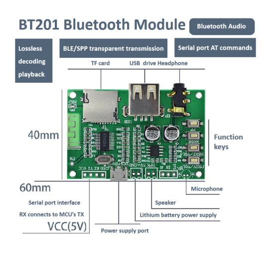
KT1025A Dual-Mode Bluetooth Audio Chip Layout Description and Design Precautions
1.Brief Overview
1. First, please refer to the provided BT201 test DEMO module as the standard.
2. If using the chip independently without testing the BT201 module and directly proceeding to layout, background noise is highly likely if experience is limited. Therefore, always compare with the manufacturer’s test board first.
3. The BT201 solution does not include FM functionality. Please note this. The FM circuit should be left floating without hesitation.
2.Precautions
1. Background noise or interference is common in Bluetooth audio products. Do not be careless during layout.
2. If you have not worked on audio products before, study online resources thoroughly. Assuming things casually will naturally lead to noise issues.
3. The core principle is to separate analog ground and digital ground. If unclear, consult an experienced engineer.
4. Ensure a clean power supply. Use an LDO whenever possible instead of a DC-DC converter.
5. Bluetooth operates at high-frequency RF and radiates energy, so some background noise is inevitable but can be minimized. With good design, noise is imperceptible to the human ear, though it may be measurable with instruments.
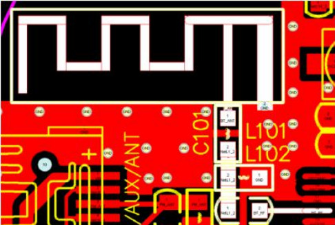
3.Antenna Description
1. For antenna and component packaging, directly refer to the PCB files of the DEMO module, available in the document library.
2. The Bluetooth antenna has no special requirements. Follow the provided package and reference instructions.
3. The Bluetooth antenna does not require impedance matching, and standard copper thickness is sufficient. Don't over complicate it—Bluetooth has a low entry barrier.
4.Power Supply Description
(1)The BT201 test board has minimal background noise, barely noticeable to the human ear.
(2)You can try powering it with a phone charger, which should not produce significant noise.
(3)Battery power is ideal as it provides pure DC and is very clean. However, consider the battery's load capacity.
(4)USB output from a desktop computer may produce significant ripple, leading to background noise. Avoid using it.
(5)If the board includes a DC-DC converter, it may cause noise. The optimal power supply is an LDO, such as a 7805.
(6)The BT201 module can drive a maximum speaker of 4 ohms, 3W with a 5V supply.
(7)When driving speakers, ensure sufficient current with a stable power supply. Insufficient current can cause speaker distortion, buzzing, etc.
(8)If possible, purchase various amplifier modules online for comparison testing. We sell Bluetooth chips, but amplifier-related noise, distortion, or other issues are extended topics that are complex and cannot be explained briefly.
5.How to check if the board has background noise?
(1)Use a clean power supply, ideally a battery, and disconnect all front-end power circuits.
(2)Connect the chip's headphone output and listen for noise. If none, check the rear-stage amplifier circuit.
(3)If USB playback has no noise but Bluetooth does, this does not necessarily indicate a problem.
(4)Use headphones to check for noise. If none, the issue lies in the amplifier section, so inspect it.
(5)If noise is present with headphones, disconnect the rear-stage amplifier and inspect the Bluetooth chip's peripheral circuits. Determine whether noise occurs during Bluetooth or MP3 playback. For Bluetooth noise, check if capacitors around the main controller are properly soldered and if they are too close to the Bluetooth module. Refer to other instructions for troubleshooting.
(6)For noise testing, avoid using a computer's USB or a charger's USB. Use a clean power supply with strong load capacity, ideally tested at 5V, not 3.7V.
6.Methods to Reduce Bluetooth Background Noise
(1)Keep the Bluetooth antenna and Bluetooth module as far as possible from analog circuits.
(2)The chip's analog ground must be connected to the power ground at the input.
(3)Check capacitors around the chip for issues such as short circuits or poor soldering.
(4)Add multiple vias to the GND of the Bluetooth section.
7.Selection and index requirements of crystal oscillators
(1)Bluetooth has high frequency offset requirements, so the crystal oscillator's quality is critical for performance. During selection, ensure consistency and stability, with a frequency deviation of ≤±10ppm and a recommended load capacitance (CL) of 12pF.
Note: Crystal-to-ground capacitors C102 = C103 = 2*CL – (4pF~6pF), where CL is the crystal's load capacitance.
(2)For designs with no size constraints, use the crystal specified in our DEMO, which is cost-effective and high-performing.
(3)For size-constrained designs, use a 24M-3225 crystal, which is slightly more expensive but performs well.
Recommendation: Use our provided crystal, which is more cost-effective and quality-assured compared to random purchases.
8.Simple PCB Layout Precautions
(1)The input voltage to LDO_IN (Pin 18 of the chip) must not exceed +5.5V.
(2)The chip must strictly separate digital GND and analog AGND (refer to the provided BT201 PCB).
(3)During PCB routing, digital GND and analog AGND must be routed separately and connected only at the battery input. If the design includes a pre-amplifier ground, connect AGND to it.
(4)All decoupling capacitors on the main controller must be placed as close as possible to the chip pins, with short ground return paths.
(5)Prioritize the placement of the Bluetooth antenna. The RF antenna must be near the board edge (or in an open area if structural constraints apply). The antenna matching circuit must be close to the RF pin, with short routing. The antenna's ground plane should follow the yellow outline in the antenna package, and the space on both sides should be as wide as possible, as shown in the diagram avove.
(6)The 24M crystal must be placed close to the chip's clock pins (BTOSCO and BTOSCI). Its routing must be shielded with a ground plane, kept away from interference sources, and not routed parallel to other data lines.
(7)Audio signal lines (DACL, DACR, AUXL, AUXR, MIC, etc.) must be routed away from digital signals (LCD/LED signals, USB, SD, etc.).
#bluetooth#audiochip#bluetoothchip#voicechip#ble#spp#electronic#coding#embeddeddevelopment#devlog#aiot
0 notes
Text
What Sets Apart a Great Electronics Design Engineer and a Top-Tier PCB Designer
Developing cutting-edge products requires more than just a basic understanding of electronics—it demands specialized expertise at multiple levels of the design process. While the roles of an electronics design engineer and a PCB designer often overlap, each discipline has its own set of core skills, priorities, and best practices. Understanding these differences can help companies build stronger teams and ensure both functionality and manufacturability from concept to production.
1: Foundations: Concept vs. Layout
Electronics Design Engineer
System-level thinking: Architects circuits that meet performance, power, and cost targets.
Component selection: An electronics design engineer chooses processors, sensors, power supplies, and other parts based on specifications and availability.
Simulation and validation: Uses SPICE, MATLAB, or custom scripts to verify that circuits behave as intended under various conditions.
PCB Designer
Physical realization: Translates schematic diagrams into board layouts, deciding component placement, routing, and layer stacks.
Signal integrity: Manages trace lengths, impedance control, and differential pairs to prevent timing mismatches and noise.
Thermal management: Integrates heat sinks, copper pours, and thermal vias to maintain reliable operating temperatures.

2: Technical Skills: Breadth vs. Depth
Breadth of Knowledge (Engineer)
A great electronics engineer understands analog and digital domains, power management, RF techniques, and often systems integration. Their toolkit includes:
Circuit simulation tools (e.g., Cadence, LTspice)
Firmware debugging (e.g., JTAG, SWD)
Test equipment (oscilloscopes, spectrum analyzers)
Depth of Expertise (PCB Designer)
A top-tier PCB designer goes deep into board stack-up design, advanced routing strategies, and material characteristics:
PCB CAD software mastery (e.g., Altium Designer, Mentor Xpedition)
High-speed design considerations (e.g., controlled impedance, crosstalk analysis)
3: Collaboration and Workflow
Communication Styles
Electronics engineers often work in cross-functional teams—mechanical, software, and compliance—to validate overall design requirements. Their deliverables include schematics, block diagrams, and simulation reports.
PCB designers interact heavily with manufacturing partners. They must document fabrication drawings, assembly notes, and BOM details clearly to avoid production delays.
By recognizing the strengths each role brings—and fostering close collaboration between them—teams can bring innovative, reliable products to market faster and more efficiently.
Source: https://extrondesignservice.blogspot.com/2025/05/what-sets-apart-great-electronics.html
0 notes
Text
Reliability and Testing of Rigid-Flex PCBs: Ensuring Long-Term Performance
Rigid-Flex PCBs are widely used in high-reliability applications such as aerospace, medical devices, military electronics, and automotive systems. These boards are exposed to constant vibration, repeated bending, temperature fluctuations, and complex assembly conditions. Therefore, reliability testing is a critical step in the design and production process to ensure long-term functionality.
This article outlines key reliability factors and common test methods used for evaluating Rigid-Flex PCBs.
Why Rigid-Flex Reliability Is Challenging
Unlike traditional rigid boards, Rigid-Flex PCBs combine materials with different mechanical properties (e.g., FR-4 and polyimide) in a single laminated structure. This introduces challenges such as:
Mechanical stress concentration in bending zones
Mismatch in thermal expansion (CTE) between rigid and flexible areas
Potential delamination during reflow or operation
Higher risk of trace cracking in dynamic-flex zones
A failure in even a single flex section can lead to total product failure — especially in critical applications where repair is not possible (e.g., implantable medical devices or aerospace systems).
Key Reliability Factors
1. Dynamic Bending Fatigue
Rigid-Flex boards are often designed to bend repeatedly during use. Poor material selection or trace layout can cause copper cracking or delamination over time.
Solution: Use rolled-annealed copper, proper bend radius (≥10x thickness), and optimized trace routing.
2. Thermal Cycling and Shock
During operation or assembly, the PCB may experience sharp temperature changes (e.g., from -40°C to +125°C), causing expansion and contraction of different materials.
Solution: Choose materials with compatible CTE, and use high-Tg laminates.
3. Moisture Resistance
Exposure to humidity can lead to resin swelling, delamination, and corrosion over time.
Solution: Use polyimide-based flex cores and perform pre-bake before reflow to remove residual moisture.
Common Reliability Test Methods
1. Bending Cycle Test (Dynamic Flex Test)
Simulates repeated folding/unfolding of the flex section. Boards are bent thousands to millions of times at defined radii and speeds.
Evaluates copper fatigue and mechanical durability
Often required for wearable electronics or foldable devices
2. Thermal Cycling Test
PCBs are exposed to repeated temperature changes (e.g., -55°C to +125°C) for hundreds of cycles.
Detects micro-cracks, delamination, and solder joint failure
Used to verify performance under real-life temperature fluctuations
3. Peel Strength Test
Measures the bonding strength between copper and the dielectric substrate (usually in the flex area).
Helps identify weak adhesive systems or poor lamination quality
4. IPC 6013 & IPC-2223 Compliance
These are industry standards that define quality and reliability expectations for Rigid-Flex PCBs.
Class 2 (General electronic products)
Class 3 (High reliability, e.g. aerospace/medical)
5. Solderability Testing
Verifies that the surface finish (ENIG, OSP, etc.) maintains good solderability after storage or thermal aging.
6. Delamination Inspection (TMA, Cross-section, or X-ray)
Checks for layer separation, resin voids, or trapped air bubbles, especially at rigid-flex transition zones.
In-Process Testing and Quality Control
During manufacturing, the following checks help prevent defects early:
AOI (Automated Optical Inspection) for outer layer pattern
X-ray inspection for BGA pads or internal vias
Flying probe or electrical testing for continuity and shorts
Visual inspection of flex transition areas and coverlay alignment
Dimensional checks to confirm outline and cutout accuracy
Final Thoughts
Rigid-Flex PCBs deliver powerful benefits in compact, high-reliability applications — but only if designed and tested properly. From dynamic flexing to thermal endurance, these boards must survive complex real-world stresses over long periods.
By implementing comprehensive testing protocols and selecting materials and structures with proven reliability, manufacturers and engineers can ensure that their Rigid-Flex products meet the highest standards of performance and safety.

0 notes