#Copper based pcb
Explore tagged Tumblr posts
Visit Tumblr Blog
Explore Tumblr blogs with no restrictions, modern design and the best experience.
Last Seen Tumblr Blogs


Fun Fact
Celebrities use Tumblr as well.
Text

What is the difference between PCB aluminum substrate and copper substrate?
PCB copper substrate: PCB copper substrate is a very expensive material among metal substrates. Its thermal conductivity is much better than that of aluminum substrate. It is suitable for heat dissipation of high-frequency circuits and precision communication equipment with large high and low temperature changes. Generally, there are gold-plated copper substrates, silver-plated copper substrates, tin-sprayed copper substrates, and anti-oxidation copper substrates.
PCB aluminum substrate: The board made of aluminum-based material is called aluminum substrate, which has strong heat dissipation ability. This type of board is commonly used in LED lighting products. Aluminum substrate is a metal-based copper-clad board with good heat dissipation function. Generally, a single-sided board consists of three layers, namely circuit layer (copper), insulation layer and metal base layer.
Email us Cynthia<[email protected]> if you are interested in PCB and PCBA service.
0 notes
Text
PCB do núcleo de cobre é um substrato de cobre + camada isolada + cobre
PCB de núcleo de cobre é um substrato de cobre + camada isolada + circuito de cobre camada PCB, também, é chamado de substrato de cobre pcb, cobre baseado pcb, cobre folheado pcb.
Um PCB base de cobre é um PCB de núcleo de metal com um substrato de cobre. Se um PCB híbrido cujo substrato é uma placa de cobre embutida na placa FR4, também é um PCB base de cobre.
#pcb fabrication#pcb manufacturer#pcb assembly#aluminium pcb#pcba manufacturing#flex pcb#pcb#pcb design#flex circuit pcb#Copper core pcb#Copper based pcb
0 notes
Text
Unlocking Innovation in Electronics: The Power of Specialized PCBs
In the world of modern electronics, printed circuit boards (PCBs) serve as the essential foundation of nearly every device, from consumer gadgets to advanced industrial systems. As technology continues to evolve, the demand for highly specialized PCBs such as blind via PCBs, ceramic PCBs, flex PCBs, copper based PCBs, and custom PCB boards has surged dramatically. These innovations not only provide enhanced performance but also meet the increasing complexity of today’s electronic applications.
In this article, we’ll explore the key types of advanced PCBs, including the benefits of working with a reliable blind vias PCB manufacturer, the importance of custom PCB manufacturers, and how these different PCB types are shaping the future of electronic product design.
What Are Blind Via PCBs?
One of the most significant advancements in PCB design is the blind via PCB. Vias are the holes that connect different layers of a multi-layer PCB. In blind vias printed circuit boards, these holes connect an outer layer to one or more inner layers without penetrating the entire board. This feature allows for a more compact and efficient layout, especially in high-density interconnect (HDI) applications.
By incorporating blind vias, engineers can increase component density without sacrificing board size or performance. This makes blind via PCBs ideal for applications such as smartphones, medical devices, and compact industrial electronics where space is at a premium.
A reputable blind vias PCB manufacturer uses laser drilling or advanced mechanical drilling to achieve precise and clean vias, ensuring optimal performance and reliability. These manufacturers often provide design support to ensure that the via placement aligns with the functional needs of the product while maintaining cost efficiency.
Ceramic PCBs: High Thermal Conductivity for Harsh Environments
Another innovative PCB solution is the ceramic PCB, which is particularly suited for high-power or high-frequency applications. These boards are made using ceramic substrates like aluminum oxide (Al2O3) or aluminum nitride (AlN), which offer excellent thermal conductivity and mechanical stability.
Ceramic PCBs are widely used in LED lighting, automotive electronics, and aerospace systems, where conventional PCBs might fail due to heat or mechanical stress. Their ability to operate in extreme conditions while maintaining electrical performance sets them apart from traditional boards.
Choosing a knowledgeable ceramic PCB manufacturer is crucial. Such manufacturers specialize in using thick film or direct bond copper (DBC) technology to create boards that can handle high temperatures and thermal cycling without degradation. Their manufacturing processes are tailored to ensure the structural integrity and thermal performance required by demanding industries.
Copper Based PCBs: Power and Durability Combined
Copper based PCBs are designed for applications where heat dissipation and current carrying capacity are critical. These boards use a thick copper layer—typically 1 oz to 10 oz per square foot—making them ideal for power supplies, automotive systems, and industrial control equipment.
The thick copper not only supports high current loads but also aids in effective heat dissipation, which extends the lifespan of both the board and its components. In power electronics, copper based PCBs are often the go-to choice due to their durability and performance.
Whether it’s single-layer or multi-layer copper boards, selecting a manufacturer with experience in copper based PCB production ensures precision in etching and lamination processes, which are crucial for maintaining electrical efficiency.
Flex PCBs: The Future of Flexible Electronics
As electronic devices become more compact and ergonomic, flex PCBs (flexible printed circuit boards) are gaining popularity. These boards are made from flexible substrates like polyimide, which allow them to bend and twist without breaking.
Flex PCBs are used in wearable technology, medical devices, and compact consumer electronics. Their unique design makes it possible to connect electronic components in tight or irregular spaces, something rigid PCBs cannot accommodate.
Unlike traditional boards, flex PCBs require special expertise in both design and manufacturing. A skilled flex circuit manufacturer will take into account factors like bending radius, dynamic flexing requirements, and signal integrity to deliver a board that performs reliably under mechanical stress.
The Importance of Custom PCB Boards
While standardized PCBs serve many applications, unique projects often require custom PCB boards designed to meet specific electrical, mechanical, or thermal requirements. A custom PCB could involve specific layout constraints, unusual form factors, or integration with other technologies like sensors or embedded antennas.
Working with an experienced custom PCB manufacturer provides access to tailored design, prototyping, and production services. Whether it’s a custom PCB board for a wearable fitness tracker or a complex multi-layer design for a satellite module, the ability to customize every aspect of the board’s structure is a key advantage in competitive industries.
Customization also enables designers to optimize the board for size, performance, and cost—something that off-the-shelf PCBs cannot provide. A good custom PCB manufacturer will work closely with engineers to understand application needs and deliver a solution that meets both technical and budgetary goals.
Choosing the Right PCB Manufacturer
With so many specialized PCB types available, it’s essential to partner with a manufacturer that offers comprehensive capabilities. Whether you’re sourcing a blind vias PCB manufacturer, a ceramic PCB manufacturer, or a supplier of flex PCB and copper based PCB solutions, the ideal partner will offer:
Advanced manufacturing technologies
In-house engineering support
Quick turnaround and low minimum order quantities
Certifications such as ISO and UL
Quality assurance testing at every stage
Partnering with a one-stop manufacturer that offers everything from custom PCB design to assembly and testing ensures a smoother production process and a higher-quality final product.
Conclusion
The electronics industry continues to push boundaries, demanding more compact, efficient, and robust solutions. From blind via PCBs that enhance space utilization, to ceramic PCBs built for harsh environments, and flex PCBs that enable groundbreaking product designs, the world of PCB manufacturing is more dynamic than ever.
Whether you're designing a next-generation wearable, an industrial automation controller, or a high-power automotive system, choosing the right type of PCB—and the right manufacturer—is crucial. Work with a proven custom PCB manufacturer that understands your needs, offers flexible solutions, and delivers on time and within budget.
By leveraging specialized boards such as blind vias printed circuit boards, ceramic PCBs, and copper based PCBs, you’re not just building a device—you’re building a competitive advantage.
0 notes
Text
You know what sucks? When you're working on a very complex and really weird spell and you just can't find the ingredients. And I can't sub them out so easily because this is a very weird spell. In short, one thing I need is a rocker switch, like the electronic component. But due to the symbolism involved, it has to be one that feels good to flip.
Might as well talk about the spell concept. Basically I'm making a magical pseudo-device, which is a physical object that doesn't function or serve a purpose physically, but has moving parts and stuff to symbolically function in a magical capacity. For example, this will have a switch that's connected to copper wires, and those wires are going to be bent and soldered into the shape of the sigil I designed for this, which will also incorporate other ingredients/materials like crystals wrapped in the wire and so on. The whole thing will be inlaid into a backing material which will basically look like a handmade magic PCB (printed circuit board, those green boards you see in electronic). The idea is that the spell in inactive until the switch is flipped, completing the circuit/sigil, and the spell will function as long as it's on, given specific conditions, it's charged/has a power source, and a killswitch isn't tripped.
I know none of this is required to make a spell like this. I could easily just draw a little sigil or make a little amulet, charge it on the windowsill and cast it when needed, but I feel like this is going to be a neat experiment. I also want to gauge the results based on amount of effort put into the spell and care taken designing and physically building it.
7 notes
·
View notes
Text
Best Partner for Wireless Modules: A Comprehensive Antenna Selection Guide
n the field of wireless communication, antenna selection is crucial. It not only affects the coverage range and transmission quality of signals but also directly relates to the overall performance of the system. Among various wireless modules, finding the right antenna can maximize their potential, ensuring stable and efficient data transmission.
When designing wireless transceiver devices for RF systems, antenna design and selection are essential components. A high-quality antenna system can ensure optimal communication distances. Typically, the size of antennas of the same type is proportional to the wavelength of the RF signal; as signal strength increases, the number of required antennas also grows.
Antennae can be categorized as internal or external based on their installation location. Internal antennas are installed within the device, while external antennas are mounted outside.
In situations where space is limited or there are multiple frequency bands, antenna design becomes more complex. External antennas are usually standard products, allowing users to simply select the required frequency band without needing additional tuning, making them convenient and easy to use.
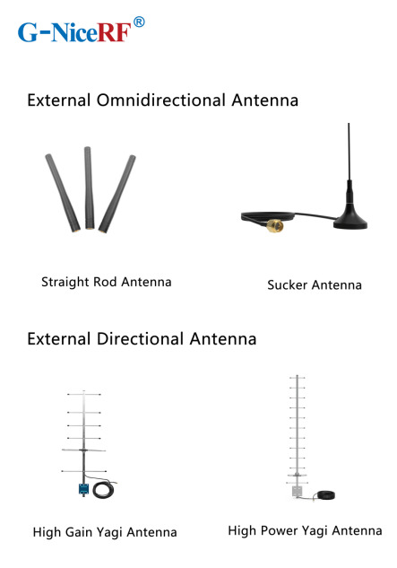
What are the main types of antennas?
External Antennas: These antennas can be classified into omnidirectional antennas and directional antennas based on the radiation pattern.
Internal Antennas: These antennas refer to antennas that can be placed inside devices.
Omnidirectional Antennas: These antennas radiate signals uniformly in the horizontal plane, making them suitable for applications that require 360-degree coverage, such as home Wi-Fi routers and mobile devices.
Directional Antennas: These antennas have a high emission and reception strength in one or more specific directions, while the strength is minimal or zero in others. Directional antennas are primarily used to enhance signal strength and improve interference resistance.
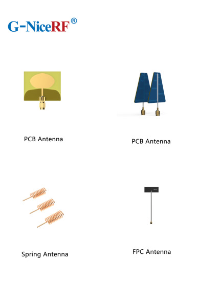
PCB Antennas: These antennas are directly printed on the circuit board and are suitable for devices with limited space, commonly used in small wireless modules and IoT devices.
FPC Antennas: FPC antennas are flexible printed circuit antennas that are lightweight, efficient, and easy to integrate.
Concealed Antennas: Designed for aesthetic purposes, concealed antennas can be hidden within devices or disguised as other objects, making them suitable for applications where appearance is important without compromising signal quality.
Antenna Selection Guide
When selecting the appropriate antenna for a communication module, it's essential to first determine whether to use an internal or external antenna based on the module's structure.
External Antennas: These antennas offer high gain, are less affected by the environment, and can save development time, but they may take up space and impact the product's aesthetics.
Internal Antennas: These have relatively high gain and are installed within the device, maintaining a clean and appealing exterior.
Sucker Antennas: These provide high gain and are easy to install and secure.
Copper Rod Sucker Antennas: Made from large-diameter pure copper radiators, these are highly efficient with a wide bandwidth.
Rubber Rod Antennas: Offer moderate gain at a low cost.
Fiberglass Antennas: Suitable for harsh environments and ideal for long-distance signal

External Directional Antennas
Typically used in environments with long communication distances, small signal coverage areas, and high target density.
Panel Antennas have high efficiency, are compact, and easy to install, while considering the impact of gain and radiation area Yagi Antennas offer very high gain, are slightly larger, and have strong directionality, making them suitable for long-distance signal transmission; however, attention must be paid to the antenna's orientation during use
Internal Antenna Selection
Most internal antennas are affected by environmental factors and may require custom design or impedance matching
Spring Antennas are cost-effective but have low gain and narrow bandwidth, often requiring tuning for good matching when installed Ceramic Patch Antennas occupy minimal space and perform well, but have a narrow bandwidth
For details, please click:https://www.nicerf.com/products/ Or click:https://nicerf.en.alibaba.com/productlist.html?spm=a2700.shop_index.88.4.1fec2b006JKUsd For consultation, please contact NiceRF (Email: [email protected]).
2 notes
·
View notes
Text
Printed Circuit Board Basics
Most of us are using Printed Circuit Board in our daily life. Printed Circuit Boards are used in almost all the Electronic products, from consumer gadgets such as PCs, tablets, smartphones, and gaming consoles to industrial and even high tech products in strategic and medical electronics domains.
Here, we have some statistics for you that shows how many electronic devices connect worldwide from 2015 to 2025. This statistic shows an increase in the use of a number of PCB in people daily life. Hence, CircuitWala took this opportunity to provide a basic knowledge about PCB via this article.
There are so many books available online which teach about Printed Circuit Board design and hardware part. There are few links available online which shows only a few basic fundamentals of PCB and few are there for Basics of Printed Circuit Board (PCB) Design. Few which gives good know knowledge on Printed Circuit Board terminology. But in the end for the hobbyist, there is no such material available which make their work easy.
Now days there few online designing websites available which allow hobbyist and students to create their design and Printed Circuit Board fabrication part. These websites provide limited features and charge high for the full edition. We, @CircuitWala are in try to provide one platform which provides plenty of Printed Circuit Board knowledge digitally to make your work simple and easy.
Alternatives of PCB include wire wrap and point-to-point construction. Creating a layout of PCB is a little bit time-consuming method as compared to its alternative solution but manufacturing of PCB is cheaper and faster then other wiring methods as electronic components are mounted and wired with one single part.
Let’s start with some basics of Printed Circuit Board with this article. Here in this article we will discuss about history of PCB to understand the emerge of PCB, Types of PCB to make your complex PCB a very simple using different types, Usage of PCB to provide you an idea to create more Printed Circuit Board projects, Advantages and Disadvantages, Possible Future to know about new technological change in Printed Circuit Board manufacturing and also about how to destroy and manage your PCB’s e-waste? We know you are eager to know all the stuff in details but before that let’s make a simple definition of Printed Circuit Board.
What is Printed Circuit Board?Printed Circuit Board is an electronic device made of conductive material(FR-4) like copper which connects components mounted on it to to get desired output by providing an input on another end.
When the board has not mounted with any of the components is called as Printed Circuit Board or Printed Wired Board. Mounting of an electronic component on Printed Circuit Board is called as PCB assembly.
History of Printed Circuit BoardThe invention of Printed Circuit Board was by Austrian engineer Paul Eisler as part of a radio set while working in England around 1936.
In early days before Printed Circuit Board became common in use, Point-to-Point construction was used. This meant some bulky and unreliable design that required plenty of sockets and regular replacement of it. Most of this issue directly address when PCB went into regular production.
Originally, every electronic component had wire leads, and the PCB had holes drilled for each wire of each component. The components’ leads were then passed through the holes and soldered to the PCB trace. This method of assembly is called Through-Hole construction. There is one other method to mount component is called as Surface Mount.
Type of Printed Circuit BoardPCBs are produced from the different types of material and on the basis of that material PCBs are divided mainly into two parts: Rigid PCB and Flexible PCB. Nowadays, a combination of Rigid and flexible PCB is also possible and that is called as Flexi-Rigid PCBs.
Most of the PCBs are built in layers. The inner layer is the base material called as a substrate. Rigid PCBs are mainly made of material like epoxy materials and Flexible PCBs are made of plastic material that can withstand high temperatures.
Rigid PCBs are generally, hard materials that hold the component in a better way. The motherboard in the tower of a computer is the best example of Rigid PCBs. Flexible PCBs fundamental material allows PCB to fit into forms that Rigid PCBs can not. Flexible PCBs can turn round without harmful the circuit on PCB.
All Rigid and Flexible PCBs can come in three formats by layers: Single Layer, Double Layer, and Multi-Layer.
1. Single Layer PCBSingle Layer PCBs have been around since the late 1950s and still dominate the world market in sheer piece volume. Single Sided PCBs contain only one layer of conductive material and are best suited for low-density designs. Single-sided PCBs are easy to design and quick to manufacture. They serve as the most lucrative platform in the industry.
2. Double Layer PCBDouble Layered printed circuit board technology is conceivably the most popular type of PCB in the industry. Double Sided PCB (also known as Double-Sided Plated Thru or DSPT) circuits are the gateway to advanced technology applications. They allow for a closer (and perhaps more) routing traces by alternating between top and bottom layers using vias.
3. Multi Layer PCB
Multilayer PCB is a circuit board that has more than two layers. Unlike a Double-Sided PCB which only has two conductive layers of material, all multilayer PCBs must have at least three layers of conductive material which are buried in the center of the material.
Usage of Printed Circuit BoardBy reading this article till this point, we hope that you are now able to get about printed circuit boards. Now, we will make you understand about different applications of printed Circuit Board.
In this digital world, Printed Circuit Board is in almost all our daily life electronic devices and in our industrial electronics as well. Below are the industries where PCBs are used:
Possible FutureNowadays, most of the circuits are replaced to produce Printed Circuit Board from the old methods. Revolution in technology made many of the processes automated and hence it is easy to manufacture PCB. But still, these processes are a bit expensive to hire, involve toxic waste and use high temperatures and acids. With technological advances we have seen in the past years, it is not hard to imagine PCB will soon be revolutionized. Not only that but research institutes predict a more ‘green’ future for PCBs; PCBs being made of paper.
Electronic Waste (e-waste)Electronic Waste or e-waste is described as discarded electrical or electronic devices. Informal processing of e-waste in developing countries can lead to adverse human health effects and environmental pollution.
Electronic scrap components contain a hazardous substance such as lead, cadmium, beryllium, or brominated flame retardants. Recycling and disposal of e-waste may involve significant risk to health of workers and communities in developed countries and great care must be taken to avoid unsafe exposure in recycling operations
Nowadays, developing countries are encouraging electronic users to take care while recycling the e-waste or submit them to the organization who are involved in such activities.
SummaryIn this blog, we have learned the basics of Printed Circuit Board. CircuitWala is planning to write as many blogs to provide more and more knowledge of Printed Circuit Board. Either it is basics or manufacturing or usages or advantages and disadvantages of PCBs. We will also try to make our users/customers up to date for the new technology innovations, including past histories and revolution of the PCB industries.
In the next blog, we will look at more briefly about the different types of Printed Circuit Board. We also understand the process to make it and different usage and application for the same.
#electronic circuit design company#pcb circuit manufacturer in ahmedabad#pcb design & manufacturing services#printed circuit board companies#printed circuit board order online#PCB manufacturer#Printed Circuited Board#double layer PCB#PCB Quality Control
2 notes
·
View notes
Text
LED PCB Assembly
What is the LED Circuit Board assembly?
Generally, LED PCB assembly is considered to be a circuit board that has the LED components soldered to it. The LED is soldered to the printed circuit board and features a chip that creates the light as electrically connected. A thermal heat sink and a ceramic base are used to bond the chip. Not all the PCB products can be used in Led industry, as an LED PCB is easy to create a high volume of heat, but making it hard to cool with traditional methods. For this reason, metal core PCB is widely used in LED application because of their enhanced ability to dissipate heat, especially aluminum pcb is often used to fabricate PCB for LED lights.
We’ve had great LED PCB assembly experiences with top LED chips to brand such as Cree, Luxeon, Osram, Nichia, Lumileds, MLS, EVERLIGHT, Samsung, LG, Seoul., etc. PCB LED lights can be incorporated into numerous lighting applications due to their combination of excellent energy efficiency, low cost and maximum design flexibility.

Application of LED PCB Assembly
Hitechpcba serves customers in different industries, providing highly reliable and innovative LED PCBs for various applications:
• Horticulture light LED PCB Assembly
• LED controller PCB Assembly
• Computer LED display and indicators
• LED lights PCB Assembly for medical use
• Automotive LED PCBs Assembly include PCBs for brake lights and headlights
• Street lighting LED PCB Assembly
• Flashlights and camping accessories
• Traffic light PCB Assembly
• Commercial lighting LED PCB Assembly
LED PCB Assembly specification
Number of layers for LED PCB
These layers are made up of aluminum and magnesium, but now have Copper base material and Ceramic base materials for LED PCB industry, we can meet it.
Aluminum LED PCBs stand out among other PCBs because it has a good insulation characteristic and has a better machinery performance, the cheap cost is one important factor too.
Types of layers for LED PCB Assembly
Normally, the base layer is made using aluminum alloy metal.
This aluminum alloy substrate used in making the base makes it ideal for through-hole technology which transfers and dissipates heat.
A thermal insulation layer is made using some ceramic polymer which has good viscoelasticity characteristics.
It is highly heat resistant and protects the PCB against heat and mechanical stress.
The circuit layer, which is covered by a copper foil which can range from one to ten ounces.
LED Board type- single or in panel
Some boards are shapeless. For this reason, LED PCB panels are used. This reduces time, labor production and testing time.
Some LED PCB Assembly is done on a single board while others are done on panel boards.
LED PCB Assembly Process
Roughly, the PCBA process can be divided into theses phases: soldering paste printing > SMT (surface mounted technology) > reflow soldering > AOI (automated optical inspection)> THT (through-hole technology) > wave soldering > touch-up and cleaning > IC-programming > FCT (functional tests) > aging testing.
Below we show you the process.
Step1. Summarizing Project Information
Before contacting your supplier, make sure you have all the project information. Suppliers will need info following for quoting LED PCB assembly:
Gerber
BOM
LED PCB specification
Quotation quantity
Once you have gathered these information, you can contact us and request for a quote.
Of course, you can also provide the schematic, LED PCB Assembly pictures and even samples to us. The more details they have, the more accurate the supplier’s quotation will be.
Step2. Discussion and details about custom LED PCB Assembly
Different projects will have different requirements. Remember the special requirements mentioned in step 1? That’s going to be the focus of this session. Equipment and engineering capacity will not be identical between suppliers. Make sure your supplier has the equipment to produce and assemble major components and the corresponding testing capabilities.
For example, some vendors don’t have X-ray testing equipment, which means they can’t check the mount quality of BGA chips. Outsourcing this step will increase risk and cost. That’s what you don’t want.
Also, pay attention to time taken by the supplier to quote. Motherboards often contain hundreds or even thousands of components, and they are supplied by different manufacturers. To ensure the quality of the components, the supplier sourcing team will make multi-inquiries from these manufacturers or authorized suppliers to match customer’s requirement, which usually takes 2-3 business days, and even longer for some scarce chips. Therefore, if your project is complex and the supplier quotes you within few hours, double check with them.
Step3. Sample and feedback
After confirming the PI, the supplier will usually provide pre-production samples for your approval. At the same time, the supplier will also confirm with you the logistics plan of the bulk goods. Make sure they understand your shipping requirements, including details on packaging, customs clearance, taxes, etc.
For us to have a successful LED PCB Assembly process, its functions must be defined. Compliance requirement is defined to reduce the effect when components are selected.
The Bill of Materials is then generated from the information installed on the LED PCB.
All this information is used to assemble components which are identified from MOB to the LED PCB.
After that, the routing of traces is determined to each component, based on the size, shape of the circuit board and location of connectors.

Hitech Circuits is trusted by thousands of electronic engineers on their LED PCB assembly projects, from consumer, led bulb to precisely medical LED light, we can help you from the beginning of design stage; From commercial flood LED to industrial high power LED, from automotive LED to military LED, Venture is the perfect place for your LED PCB assembly requirement.
Hitech Circuits has been participated in hundreds and thousands of LED lighting projects, by providing LED PCB and also LED PCB assembly service.
Our LED PCB assembly had covered both ends of the Lighting Class LED size spectrum, assembling some of the largest (2 meter long boards) and some of the smallest LED Lighting applications which used in Medical Endoscopes.
LED PCB Assembly is very crucial in the current industrial development. Many electrical devises are being innovated and the old once being improved.
LED PCBs are useful due to the fact that they are made using materials that can transfer and dissipate heat. This characteristic increases device durability.
The world is changing with new technology, especially PCB technology that plays an essential role in the application of LED circuits. And the LED industry is taking advantage of this technology and growing faster.
As a full feature PCB solutions provider with more than a decade of experience, we're capable to provide LED PCB fabrication, components procurement and LED PCB assembly all under one roof. We can work with you to develop metal core PCB, aluminum circuit boards customized to your specific applications. We feature competitively priced PCBs made with standard FR-4 material that includes a thermal aluminum clad layer that will efficiently dissipate heat, keep all LED PCB components cool and significantly enhance the performance of your products.

LED pcb board, LED pcb assembly
LED with its advantages of high brightness, high efficiency, low heat, long life, is considered the most development potential in the 21st century lighting. In the market and policy driven by the rapid development of the domestic LED industry blowout has formed a relatively complete industrial chain, including the production of epitaxial wafers, chip preparation, packaging, integration, LED application. In 2010, China's LED industry scale, up from $ 827 billion in 2019 to 220 billion yuan, an annual growth rate of over 70%, higher than the 50% level of growth of the global LED lighting industry output value. Among them, the middle and lower reaches of the most complete industrial chain, accounting for 90% of the overall percentage of the GDP.Chinahas become the world's leading LED manufacturing base and important application market.
To further promote the technological innovation of the LED industry, construction and wide application of independent industry chain, China Electronic Appliance Corporation and industry associations to organize the theme of "Focus on the core energy LED Exhibition will be held November 9-11, 2010 in Shanghai International Expo Center and the 78th China Electronics Fair over the same period will be held will create from raw materials, epitaxial wafers, chip, LED bracket, LED accessories, LED packaging and supporting materials, the LED backlight upstream firm to the upstream and downstream enterprises of the display, lighting, landscaping, decorative lighting, traffic lights, automotive lighting, special lighting, to the equipment, instrumentation, software, finance, consulting and other service enterprises and technological exchanges and market trading platform, help the domestic industry sustained and healthy development, and promote the steady expansion of the LED application market.
In the LED industry chain upstream of the epitaxial wafers and LED chips accounted for 70% of the profits of the whole industry, and technology-intensive, capital-intensive, where the core technology of the LED. Well-known epitaxial wafer and chip production enterprises will be exhibited a number of energy-efficient, low heat, cost-effective LED products, many of whom have excellent products of international advanced level.
LED electronic pcb assembly manufacturing 100% Original LED Chip with one-stop in-house pcba services
3 notes
·
View notes
Text
Top 15 PCB Board Manufacturers in USA

When it comes to building reliable electronics, choosing the right PCB board manufacturer in USA is critical. Whether you’re a startup, engineer, OEM, or tech company, having a dependable partner for printed circuit board fabrication and assembly ensures faster production, fewer errors, and better results.
In this blog, we list the Top 15 PCB board manufacturers in the USA known for high-quality PCB fabrication, assembly, and fast delivery. These companies are widely searched and trusted across various industries — from medical to aerospace, IoT, automotive, and industrial applications.
1. PCB Power
PCB Power is one of the most trusted names among PCB board manufacturers USA. With over two decades of industry experience, PCB Power offers quick-turn PCB fabrication, full turnkey assembly, and components sourcing — all under one roof.
As a USA-based PCB company, they focus on delivering high-quality single, double, and multilayer PCBs with fast turnaround and competitive pricing. Whether you’re building prototypes or mass production, PCB Power’s online ordering system makes it easy to get instant quotes, track orders, and communicate with real engineers.
Key Features:
US-based production for fast and reliable delivery
ISO-certified processes for superior quality
Advanced manufacturing for high-density, multilayer PCBs
Turnkey assembly and BOM handling
Expert support for startups, engineers, and OEMs
If you’re looking for a complete PCB manufacturing solution in the USA, PCB Power should be your first stop.
2. Advanced Circuits
Advanced Circuits is one of the largest and oldest PCB manufacturers in the United States. Known for high-quality prototypes and low-to-medium volume production, they serve industries like aerospace, defense, and telecom.
They offer same-day and next-day shipping options and have their own in-house manufacturing for consistent quality.
3. Sierra Circuits
Sierra Circuits is a full-service PCB company specializing in quick-turn fabrication and assembly. They’re well-known for their high-performance HDI PCBs, rigid-flex boards, and support for complex designs. Sierra Circuits is ideal for companies looking for technical precision and tight tolerances.
4. Sunstone Circuits
Sunstone Circuits has built a reputation for delivering reliable prototype PCBs and small-batch orders. Their online design tools and instant quote system are ideal for hobbyists, startups, and small engineering teams. Their US-based manufacturing ensures high quality and fast shipping.
5. Bay Area Circuits
Located in California, Bay Area Circuits serves the Silicon Valley tech community with rapid prototyping, fabrication, and assembly services. They are experts in small-run production and serve various industries including medical, aerospace, and communications.
6. Rush PCB Inc.
Rush PCB Inc. offers full turnkey PCB services, including design, manufacturing, and assembly. They specialize in multilayer, flex, and rigid-flex PCBs with quick-turn options. Their experienced team supports everything from prototypes to volume production.
7. Custom Circuit Boards
Based in Arizona, Custom Circuit Boards provides high-quality PCBs for engineers and hardware startups. They focus on fast production and specialize in multilayer boards, thick copper PCBs, and RF designs.
8. Imagineering Inc.
Imagineering Inc. offers both PCB fabrication and assembly with ISO 9001 and AS9100 certifications. They serve demanding industries like medical and aerospace and are known for excellent quality and fast lead times.
9. Epec Engineered Technologies
Epec is a full-service provider offering custom PCB manufacturing, flexible circuits, and battery packs. With decades of experience, they provide engineered solutions for complex applications and tight deadlines.
10. APCT Inc.
APCT is known for high-speed, high-density interconnect PCBs. They support quick-turn and production-scale manufacturing. Their specialties include aerospace and defense-grade boards with rigorous quality requirements.
11. OnBoard Circuits
OnBoard Circuits offers affordable PCB prototyping, fabrication, and assembly with domestic and offshore capabilities. They are known for great customer support and fast delivery for small to medium volume orders.
12. Millennium Circuits Limited (MCL)
MCL provides reliable PCBs including rigid, flex, and rigid-flex boards. They serve industries like telecom, industrial, and medical, offering fast turnaround times and excellent pricing.
13. TechnoTronix
TechnoTronix offers advanced PCB manufacturing and assembly solutions with a strong focus on precision and fast lead times. They work with both small businesses and large enterprises, offering everything from basic to complex PCB designs.
14. RedBoard Circuits
RedBoard Circuits provides quality PCBs with a focus on customer service and quick delivery. They offer a wide range of PCB types including FR4, aluminum, and Rogers materials.
15. ALLPCB USA
ALLPCB USA offers cost-effective PCB solutions with a quick-turn focus. They provide both prototype and production runs and serve customers looking for affordable yet reliable circuit boards.
Choose the Best PCB Manufacturer for Your Needs
Selecting the right PCB board manufacturer in USA can be the difference between a successful project and costly delays. Whether you need fast prototyping, volume production, or full turnkey PCB assembly, each of these top 15 manufacturers brings something unique to the table.
However, if you’re looking for a complete solution with fast delivery, reliable quality, and competitive pricing — PCB Power is a clear leader. With US-based manufacturing, expert support, and a user-friendly online ordering platform, PCB Power makes your PCB journey seamless from design to delivery.
0 notes
Text
PCBA: The Silent Backbone of Electronic Devices
Printed Circuit Board Assembly (PCBA) serves as the critical foundation for nearly every electronic device in our modern world. From smartphones and laptops to industrial automation systems and aerospace equipment, PCBA ensures that the various electronic components within a device function smoothly and cohesively. Its precision and reliability are not just technical necessities but vital to sustaining innovation in the global tech economy.Get more news about PCBA manufacturer,you can vist our website!
Understanding PCBA
At its core, PCBA refers to the process of soldering electronic components onto a printed circuit board (PCB). While a PCB is simply the board with copper traces that connect components electrically, the assembly process transforms it into a fully functional circuit. This involves mounting integrated circuits (ICs), resistors, capacitors, diodes, and other components using either Surface Mount Technology (SMT), Through-Hole Technology (THT), or a hybrid of both, depending on the design and purpose of the device.
The PCBA Process
The process typically begins with solder paste application, where a stencil is used to apply the paste on predefined areas of the PCB. Automated pick-and-place machines then accurately position the tiny components onto the board. This is followed by reflow soldering, where the board is passed through a controlled oven to melt the solder and secure the components.
For boards requiring through-hole components, manual or wave soldering is used. Once soldered, the board undergoes inspection and testing—ranging from Automated Optical Inspection (AOI) to X-ray analysis and functional testing—to ensure quality and performance. Advanced PCBA plants employ high levels of automation, drastically reducing human error and improving output consistency.
Applications Across Industries
PCBA's influence stretches far beyond consumer electronics. In the automotive sector, it powers systems ranging from infotainment units to electric vehicle battery management. In healthcare, PCBA-based medical devices like ECG machines and portable monitors are critical to patient diagnostics and care. Aerospace and military applications demand high-reliability PCBA to function under extreme environments—an area where rigid quality controls and testing standards become indispensable.
Trends and Innovations
The PCBA landscape continues to evolve rapidly with advances in miniaturization, multi-layer boards, and flexible circuits. With the rise of the Internet of Things (IoT), demand for compact, power-efficient, and wireless-capable assemblies has exploded. Manufacturers are investing in smart factories, using AI-driven inspection and robotics to further optimize production.
Meanwhile, environmental considerations are pushing green manufacturing methods, such as lead-free solder and recyclable board materials. Companies are also embracing design-for-manufacturing (DFM) principles to streamline assembly and minimize waste.
Conclusion
Though rarely visible to end-users, PCBA is the invisible force driving the electronics revolution. Its blend of engineering precision, automation, and innovation enables the digital tools and systems we rely on daily. As global technology continues to push boundaries, PCBA will remain the structural and functional heart of that progress—quietly pulsing behind every screen, circuit, and sensor.
0 notes
Text
Reliable Metal Clad PCB Suppliers in India: Vaishnavi Electronics at the Forefront of Innovation
As the electronics industry moves toward higher power and thermal efficiency, Metal Clad PCBs (MCPCBs) have become an essential component in modern electronic design. Known for their superior heat dissipation, durability, and performance in high-power applications, MCPCBs are widely used in LED lighting, automotive electronics, power converters, and industrial equipment. In India, Vaishnavi Electronics stands out as one of the most dependable metal clad PCB suppliers, known for its quality manufacturing, technical expertise, and customer-centric approach.
The Strategic Importance of Metal Clad PCBs in High-Power Applications
Metal Clad PCBs, often composed of a thermally conductive dielectric layer sandwiched between a metal base (typically aluminum or copper) and a copper circuit layer, are engineered to manage heat more efficiently than standard PCBs. Their ability to draw heat away from active components ensures longer lifespan, higher reliability, and improved performance in thermally demanding environments.
Unlike traditional PCBs, MCPCBs allow designers to use higher power densities and compact layouts without compromising thermal performance. They are particularly valuable in LED lighting systems, where excessive heat can degrade performance, as well as in power supply units, motor controllers, and RF applications.
As demand for energy-efficient and high-performance devices increases, so does the need for advanced PCB solutions like metal clad boards. This has positioned quality suppliers like Vaishnavi Electronics as critical partners for OEMs and electronics manufacturers across sectors.
Vaishnavi Electronics: Trusted Partner for Custom Metal Clad PCB Solutions
Vaishnavi Electronics, based in India, has earned a reputation as a leading supplier of metal clad PCBs, offering reliable and tailored solutions that meet the specific needs of its clients. The company has invested in advanced manufacturing processes and quality control systems to ensure consistent production of high-performance MCPCBs.
With capabilities to work on various metal substrates—such as aluminum, copper, and steel—Vaishnavi Electronics supports a wide range of applications, from LED modules to power management systems. The company’s expertise extends beyond standard offerings; it provides customized MCPCB solutions, including multi-layer constructions, specific thermal conductivity requirements, and design support for complex layouts.
Vaishnavi’s production process emphasizes durability, thermal stability, and electrical integrity. Every MCPCB undergoes rigorous testing to ensure it meets industry standards for thermal resistance, mechanical strength, and electrical performance. Additionally, their engineering team works closely with clients to optimize board layout for maximum efficiency and reliability.
What sets Vaishnavi Electronics apart is not just its technical know-how but its commitment to customer service. Whether it's rapid prototyping or bulk production, the company delivers on time, offering competitive pricing without compromising on quality.
In conclusion, the growing demand for Metal Clad PCB suppliers across high-power and thermally challenging applications highlights the need for experienced and dependable suppliers. Vaishnavi Electronics continues to lead the way in India’s PCB industry with its advanced capabilities, customized solutions, and unwavering focus on quality. For businesses seeking a trusted partner in metal clad PCB supply, Vaishnavi Electronics offers a strategic advantage through innovation, reliability, and precision manufacturing.
Visit:- https://www.vaishnavielectronics.co.in/metal-clad-pcb.html
0 notes
Text
Before laminating multi-layer boards or base materials, it is necessary to align and stack inner layers, prepregs, copper foils, and other loose materials with steel plates, kraft paper padding, etc., to ensure accurate alignment (registration). This preparatory work before sending the materials to the laminating machine for hot pressing is called panel layout.
0 notes
Text

LED copper Base PCB, components assembly manufacturer in China, Hitech Circuits
Product type: 1 Layer Metal Base LED PCB
Material Copper: base
Layers/thickness: 1L/2.0mm
Line Space/width: 20/16mil
Surface treatment: Immersion gold
Minimum hole dia.: 1.5mm
Outer Layer Copper Thickness: 1/1 OZ
Email us Cynthia<[email protected]> if you are interested in PCB and PCBA service.
0 notes
Text
Rigid-Flex PCB Design Guidelines: Ensuring Reliability and Manufacturability
Designing a Rigid-Flex PCB requires more than just combining rigid and flexible sections into one board. It involves careful planning of layout, layer structure, materials, and mechanical constraints to ensure the final product is reliable, manufacturable, and cost-effective.
Below are key guidelines every engineer should follow when designing Rigid-Flex PCBs.
1. Define Rigid and Flex Zones Early
Clearly identify the rigid and flex areas during the initial layout phase. Flex regions should only exist where necessary — overdesigning with too much flex area increases cost and complexity.
Each zone should be planned based on:
Mechanical movement (bending/folding)
Component placement needs
Connector and housing locations
Avoid placing unnecessary flex areas just for routing convenience unless absolutely needed.
2. Maintain Symmetrical Layer Stack-Up
An unbalanced stack-up can lead to warping, twisting, or delamination during lamination or reflow.
Keep the number and thickness of layers symmetrical around the centerline of the rigid section.
Use dummy traces or copper balancing layers to achieve mechanical balance if needed.
Plan separate stack-ups for rigid and flex areas, but ensure transition is smooth.
3. Protect the Flex Area
The flexible section is vulnerable to cracking and wear if not designed carefully.
Never place vias, pads, or components in the flex zone.
Maintain generous spacing between traces in the flex area to reduce mechanical stress.
Avoid 90° corners and sharp transitions — use smooth curves or teardrops for trace routing.
Use coverlay (instead of solder mask) to protect the flex area from mechanical damage.
4. Follow Proper Bending Design Rules
The flex section must withstand multiple bends over its lifetime. Improper bending design can cause trace cracking, delamination, or copper fatigue.
Minimum bend radius should be 6 to 10 times the flex thickness for dynamic bends.
For static (one-time) bends, 3 to 6 times the thickness may be acceptable.
Use curved traces in the bend area to avoid concentration of stress.
Keep traces perpendicular to the bend axis wherever possible.
5. Stiffener Usage
Stiffeners are added in flex areas to provide mechanical support for connector pads or component locations.
Use FR4, polyimide, or stainless steel stiffeners depending on mechanical requirements.
Clearly define stiffener thickness and position in the mechanical drawings.
Do not overlap stiffeners with bend areas unless absolutely required.
6. Routing and Trace Layout
Trace layout impacts both electrical and mechanical performance.
In the flex region, use wide, evenly spaced traces to reduce stress.
Avoid overlapping traces on top and bottom layers in bend areas.
Do not route traces over the transition zone between rigid and flex — leave a clearance buffer.
Maintain consistent impedance and routing lengths for high-speed signals.
7. DFM Considerations
Design for Manufacturability (DFM) is critical for Rigid-Flex PCBs due to the multiple lamination cycles and tighter tolerances.
Ensure design files clearly mark flex/rigid regions and bending direction.
Avoid complex via structures (like stacked or blind/buried vias) near flex zones.
Confirm with the PCB manufacturer about acceptable layer counts, material systems, and bend performance.
Work closely with your fabricator early in the design process to avoid costly revisions.
8. Assembly Planning
Plan your PCB assembly process around the flex structure.
Use support fixtures or carrier panels during SMT to keep the board flat.
Make sure flex areas are protected during handling and soldering.
Define handling instructions clearly if the flex zone should not be bent before final assembly.
Final Thoughts
Rigid-Flex PCBs offer unmatched versatility for compact, high-performance designs — but only when designed correctly. By following key guidelines for stack-up, routing, bending, and assembly, designers can ensure their boards are reliable, manufacturable, and optimized for long-term success.
Collaborate closely with your PCB manufacturer and assembly house throughout the design process to turn your concept into a robust, production-ready product.
0 notes
Text
What Is Brass Sheet, Copper Sheet & the Best Metal for Reliable Performance?

Introduction: The Backbone of Quality Fabrication
From industrial workshops to architectural design studios, choosing the right sheet metal determines the quality, functionality, and longevity of your work. Whether you're crafting durable components, elegant fixtures, or high-precision parts, materials like the brass sheet, copper sheet, and globally trusted imported products stand out for their reliability.
In this blog, we’ll explain what each material is, where it’s best used, and how to select the best sheet metal for reliable performance in any project.
What Is a Brass Sheet?
A brass sheet is a flat-rolled alloy of copper and zinc, appreciated for its durability, corrosion resistance, and decorative appeal. It is used in both engineering and design contexts due to its strength and golden finish.
✔ Features of Brass Sheet:
Visual Appeal: Bright, gold-like appearance perfect for design
High Workability: Easily bent, cut, or engraved
Corrosion Resistance: Withstands moisture and salt air
Smooth Surface: Ideal for etching or engraving
✔ Best Uses:
Architectural hardware and design panels
Plumbing components and valves
Marine applications and instruments
Engraved nameplates and display boards
Choose from premium Brass Sheet options ideal for aesthetic and industrial-grade applications.
What Is a Copper Sheet?
A copper sheet is made from high-purity copper and is known for its excellent thermal conductivity, electrical properties, and antimicrobial capabilities.
✔ Why It’s Preferred:
Unmatched Conductivity: Ideal for electrical applications
Thermal Efficiency: Used in cooling and heating systems
Antimicrobial Surface: Makes it hygienic for healthcare and kitchens
Aging Gracefully: Forms a beautiful patina for weathered looks
✔ Best Applications:
Switchboards, wiring plates, and PCB boards
Copper roofs, domes, and flashings
Countertops, wall claddings, and kitchen surfaces
Renewable energy units and HVAC systems
Get certified and versatile Copper Sheet trusted across electrical and sanitary industries.
What Are Imported Products in Sheet Metal?
Imported products refer to high-grade metal sheets sourced from international manufacturers, known for their tight tolerance, premium finish, and global certifications like ISO, ASTM, and DIN.
✔ Advantages of Imported Sheets:
Global Compliance: Meets international quality standards
Superior Surface Quality: Available in mirror, matte, brushed, or coated
Specialty Materials: Includes bronze, nickel silver, and other alloys
Perfect for Automation: Ready for CNC, laser, and hydraulic presses
✔ Best Industrial Uses:
Aerospace components and instrumentation
Luxury architectural interiors and elevators
Medical equipment, enclosures, and consoles
High-end export products requiring consistent quality
Explore globally compliant Imported Products for quality that meets international demand.
What Is the Best Sheet for Reliable Results?
Here’s a quick guide comparing your three material options for performance: CategoryBrass SheetCopper SheetImported ProductsVisual AppealElegant Gold FinishRich Reddish ToneCustomizable (Mirror, Matte)Electrical UseModerateExcellentDepends on grade/alloyMechanical StrengthHighHighExtremely HighCertificationsIS/BISBIS/ASTMISO, ASTM, JIS, DINWeather ResistanceHighVery HighVaries (coated or alloy-based)
What Is the Best Thickness for Industrial Use?
Sheet thickness determines mechanical strength, weight capacity, and application suitability.
0.3 mm – 1 mm: Ideal for electronic panels, art, and interior cladding
1 mm – 3 mm: Best for furniture hardware, roof sheets, machine covers
3 mm – 6 mm+: Used in structural, load-bearing, or high-voltage systems
Imported sheets offer tight tolerance precision, making them excellent for robotic and automated use.
What Is the Best Surface Finish for Reliable Results?
Surface finish affects corrosion resistance, appearance, and post-fabrication effort. Finish TypeIdeal ForMirror PolishInteriors, nameplates, hotel lobbiesBrushed FinishKitchens, signage, elevatorsMatte FinishIndustrial or minimalist architectural stylesEmbossed/LaminatedDecorative and outdoor-use sheets
Imported products come pre-finished, which saves cost and ensures factory-grade consistency.
What Is the Best Way to Maintain Sheet Metal Performance?
✔ Storage Tips:
Keep flat with protective layers in low-humidity environments
Separate sheets with foam or plastic to prevent scratches
Avoid contact between dissimilar metals to prevent galvanic corrosion
✔ Maintenance Tips:
Brass Sheet: Clean with brass polish or a lemon-vinegar mixture
Copper Sheet: Let natural patina develop or use copper polish
Imported Sheets: Follow specific finish guidelines; avoid abrasive cleaning
Final Thoughts: Choose Materials That Stand the Test of Time
Choosing between a brass sheet, copper sheet, or imported products isn’t just about price—it’s about long-term performance, safety, and visual appeal. Brass offers beauty and corrosion resistance. Copper brings conductivity and hygiene. Imported materials offer global standards, precision, and versatility.
0 notes
Text

How is Aluminum PCB Made?
1. Material Selection: The primary material for Aluminum PCBs is an aluminum alloy, which acts as the base. This is paired with a thermally insulating layer and then a copper foil. The type of aluminum, insulating material, and copper thickness can vary based on the application.
2. Lamination: The layers are laminated together using heat and pressure. This ensures that the copper foil adheres well to the insulating layer, which in turn is bonded securely to the aluminum base.
3. Circuit Pattern Printing: Once laminated, the desired circuit pattern is printed onto the copper foil using a special ink. This ink acts as a protective barrier in the subsequent etching process.
4. Etching: The board is then subjected to an etching solution. This solution removes the exposed copper, leaving behind only the circuit pattern protected by the ink.
5. Drilling: Holes are drilled into the PCB for component leads or vias. This is done using precise CNC machines to ensure accuracy.
6. Surface Finish: To protect the exposed copper circuitry and improve solderability, a surface finish is applied. Common finishes include HASL (Hot Air Solder Leveling), ENIG (Electroless Nickel Immersion Gold), and OSP (Organic Solderability Preservatives).
7. Solder Mask Application: A solder mask is applied over the circuitry, leaving openings only where soldering will occur. This mask prevents accidental solder bridging during assembly.
8. Silkscreen Printing: For ease of assembly, reference designators and other important information are printed onto the PCB using ink.
9. Testing: Before shipping, the PCBs undergo electrical testing to ensure there are no shorts or open circuits.
10. Cutting and Profiling: The PCBs are then cut from the larger panel and profiled to the desired shape.
11. Final Inspection: A thorough visual inspection is done to ensure the PCB meets all quality standards.
The above process is a general overview, and specific processes will vary depending on the manufacturer and the intended application of the PCB.
0 notes
Text

Aluminium PCB
Aluminium PCB are metal-based, copper-clad laminates with a good heat dissipation function. Usually, Aluminium PCB is refer to LED PCB board, which is the most important part of LED display and lighting products, etc.
Hitech Circuits Co., Limited is a professional aluminum pcb board, LED PCB manufacturer in China. Through 10 years of aluminum pcb board designing and manufacturing experience, Hitech are able to provide high quality and cost effective single layer, double layer and multi layer aluminum pcb boards to global customers. For any of your requirements regarding aluminum pcb board, please don’t hesitate to contact [email protected]
#Aluminium PCB#aluminum pcb#pcb assembly#pcb#engineering#technology#pcba#pcb manufacturer#pcbassembly#pcb design#hardware
5 notes
·
View notes