#Customized PCB Boards
Explore tagged Tumblr posts
Visit Tumblr Blog
Explore Tumblr blogs with no restrictions, modern design and the best experience.
Last Seen Tumblr Blogs


Fun Fact
Tumblr has been banned in Indonesia for providing people with access to pornographic content.
Text
PCB Manufacturing

PCB manufacturing is a precision process involving designing, etching, and assembling printed circuit boards. We specialize in producing high-quality PCBs tailored to your specifications. Our advanced technology and rigorous quality control ensure reliability and performance. Trust us for efficient and cost-effective PCB manufacturing solutions to meet your electronic needs.
Visit Our Site: https://sqpcb.com/products/pcb-manufacture
#customized pcb boards#customize pcb#pcb board#pcb china#aluminium pcb board#multilayer pcb#printed circuit board#aluminum base pcb#circuit board#custom circuit boards
0 notes
Text
Viasion PCB: Your Trusted Partner for High-Quality Custom and Advanced PCBs
In today’s fast-paced electronics industry, choosing the right PCB manufacturer can make all the difference. Whether you're working on a new tech innovation or scaling an existing product, the quality, precision, and reliability of your printed circuit boards are critical. That’s where Viasion Technology Co., Ltd. steps in—a proven leader in the PCB industry with over 15 years of experience delivering excellence.
Viasion offers comprehensive PCB manufacturing and assembly services to clients across the globe, including the United States. From custom PCB boards to complex blind vias printed circuit boards, their products serve various industries including automotive, telecom, medical devices, and consumer electronics.
Why Choose Viasion for Your PCB Needs?
Viasion is more than just a custom PCB manufacturer. Their expertise spans across a wide range of advanced PCB types including blind via PCBs, ceramic PCBs, flexible PCBs, and copper based PCBs—all manufactured in ISO-certified facilities with stringent quality control.
Here’s a closer look at what makes Viasion a preferred partner:
1. Advanced Blind Via PCB Capabilities
For high-density interconnect (HDI) designs, blind vias PCBs are essential. These vias connect outer layers to inner layers without passing through the entire board, saving space and improving signal integrity. As a trusted blind vias PCB manufacturer, Viasion delivers precise, reliable blind via PCBs ideal for compact, high-speed devices.
Their expert team uses laser drilling and advanced lamination techniques to ensure accuracy and consistency in every board. Whether you're prototyping or in full-scale production, Viasion provides solutions that meet your specific requirements.
2. Durable and High-Performance Ceramic PCBs
When it comes to thermal conductivity, high-frequency performance, and durability, ceramic PCBs stand out. Ideal for aerospace, LED lighting, and automotive applications, these boards handle extreme environments where standard PCBs may fail.
As an experienced ceramic PCB manufacturer, Viasion offers a variety of ceramic substrates, including alumina and aluminum nitride, ensuring optimal performance even in the most demanding conditions. Their ceramic PCBs are designed to offer low thermal expansion, excellent insulation, and high mechanical strength.
3. Cost-Effective and Efficient Copper Based PCBs
Copper based PCBs are essential for high-power electronics due to their superior heat dissipation capabilities. These are commonly used in power converters, industrial control systems, and automotive components.
Viasion manufactures copper based PCBs with excellent reliability and durability. Their manufacturing process ensures a strong bond between copper and insulating layers, resulting in high-performance boards ready for tough applications.
4. Fully Customizable PCB Manufacturing
Need something tailored to your specific project? Viasion is a specialist custom PCB manufacturer, delivering bespoke PCB solutions that match your design and functional requirements. Whether it's a custom PCB board for a wearable device or a multi-layer board for an IoT product, their engineering team works closely with you to bring your design to life.
You’ll get DFM (Design for Manufacturing) support, fast prototyping, and competitive pricing—all while maintaining the highest quality standards.
5. Reliable Flexible PCB Manufacturing
For applications where space, weight, and flexibility are crucial, flexible PCBs are the go-to solution. Used in devices like smartphones, cameras, and medical instruments, flexible PCB boards allow for bendable, compact designs.
Viasion is a trusted flexible PCB manufacturer, producing single-sided, double-sided, and multi-layer flex PCBs. Their flex PCB capabilities include fine-line spacing, tight tolerances, and advanced materials like polyimide for high heat resistance.
Their flexible circuits are tested for bend cycles, ensuring longevity and reliability even under constant motion and mechanical stress.
Applications Across Every Industry
Viasion serves a wide array of industries:
Medical Devices: Miniaturized flexible PCBs and ceramic PCBs for diagnostic tools and implants
Automotive: High-temperature copper based PCBs and custom PCBs for control units
Consumer Electronics: High-density blind via PCBs and flexible PCBs for wearables and mobile devices
Telecommunications: Multi-layer custom PCBs and blind vias printed circuit boards for routers and servers
Industrial Equipment: Rugged ceramic PCBs and copper based PCBs for control systems
No matter your industry, Viasion brings the technical expertise and manufacturing excellence needed to make your project a success.
Why U.S. Customers Trust Viasion
Even though Viasion is based in Shenzhen, China, their services are perfectly aligned for U.S. businesses. With fast international shipping, English-speaking support staff, and a focus on total customer satisfaction, Viasion delivers a seamless experience for customers in the United States.
Key benefits for U.S. clients include:
No minimum order quantity
Quick turnaround and prototyping
Full turnkey PCB assembly service
Competitive pricing without compromising quality
UL and ISO certified production processes
Get Started Today
Whether you need a custom PCB board, ceramic PCB, or a complex blind vias PCB, Viasion is equipped to deliver top-tier solutions tailored to your unique specifications. Their dedication to quality, innovation, and customer support makes them the go-to custom PCB manufacturer for companies across the USA and beyond.
👉 Visit www.viasionpcb.com to request a quote or reach out to their team at [email protected] for personalized support.
0 notes
Text
The Rise Of Flexible And Foldable Pcbs In Consumer Electronics

The technological transition occurring inside electronic devices matches the fast pace of changing devices themselves in modern times. The evolution of consumer electronics receives transformative power through the development of flexible , foldable custom PCB board. Flexible circuit boards break traditional electronic design rules when they are produced for sleek modern electronics that become easily integrated into everyday use. Flexible PCBs serve as the core elements that allow smartphones to open and close while wearable fitness trackers match the human wrist shape.
1. The Evolution from Rigid to Flexible
Device designs were constrained to boxy shapes by the inflexible, flat nature of traditional PCBs. The requirement for electronics to fit into increasingly small and unusually shaped goods marked the beginning of the road toward flexibility. In order to allow circuits to bend without breaking connections, engineers created materials and manufacturing processes. It took years of development into conductive materials that could sustain repetitive flexing without losing their electrical integrity for this evolution to occur.
2. Space-Saving Advantages in Modern Devices
Electronic gadgets' use of space has been transformed by the capacity to fold and bend circuitry. Every millimeter matters in the cutthroat world of consumer electronics. Flexible PCBs can be curved to fit asymmetrical spaces that would otherwise go unused, folded into small configurations, or stacked in three dimensions. Manufacturers may either reduce the overall size of devices or fit more functions into the same footprint thanks to this space efficiency. Modern smartphones, for instance, can have more cameras, bigger batteries, and more features while still having thin profiles because flexible circuit designs save space.
3. Enabling New Form Factors and Designs
The rise of whole new device categories is arguably the most obvious effect of flexible PCBs. Without circuitry that can repeatedly bend at the hinge without degrading, foldable cell phones that open into tablet-sized screens would not be feasible. Circuit boards that can take on non-flat designs are also necessary for electronic fabrics, wraparound displays, and curved-screen televisions. Because the electronics may now adapt to the ideal product shape, product designers are no longer compelled to construct devices around inflexible rectangular boards. This paradigm change promotes industrial design innovation by enabling businesses to investigate organic shapes that are more conducive to human interaction.
4. Enhanced Durability and Reliability
Contrary to popular belief, flexible PCBs frequently perform better in durability testing than their rigid counterparts. When exposed to physical shock or vibration, traditional rigid boards might crack, leading to connection failures and irreversible damage. Flexible circuits, on the other hand, can withstand shocks by gradually deforming and then reverting to their initial state. They are perfect for portable gadgets that are subjected to drops or bumps on a regular basis because of their natural shock resistance. Furthermore, because flexible PCBs may be produced as a single continuous circuit, numerous solder joints that serve as failure spots in traditional designs are eliminated, resulting in fewer interconnection points overall.
5. The Role in Wearable Technology Growth
The wearable technology industry has expanded during the past years to make smartwatches and fitness trackers together with health monitors commonplace consumer items. The evolution of flexible printed circuit boards that could conform to human body contours would have limited the growth in this field. Devices used for prolonged wear require flexible features which rigid electronics technology cannot reproduce. The flexible nature of these circuits allows devices to match human body movements and maintain stable contact with the skin for accurate biometric monitoring and prevent any unwanted pressure on the skin. Flexible PCB technology enables wearable devices to stay discreet in daily life because their low weight reduces overall device mass.
6. Manufacturing Challenges and Innovations
Manufacturing processes experienced crucial developments due to the specific difficulties in producing flexible PCBs. Certain raw materials with particular manufacturing methods must be utilized to produce bendable conductive components. Manufacturers use modern printing technologies to establish new methods of tracing conductive tracks on flexible surfaces instead of using traditional etching methods. Traditional fiberglass boards resist heat damage better than flexible materials therefore maintaining proper assembly temperature remains essential. The production of flexible circuits has produced both specialized tools and procedures because of these technical obstacles. Flex PCB engineering technology that was previously reserved for high-end products because of manufacturing costs now reaches reasonable prices for consumer electronics through ongoing advancements and market scalability factors thus driving manufacturers to replace rigid circuitry.
7. Environmental and Sustainability Benefits
Compared to conventional rigid boards, flexible PCBs have a number of environmental benefits. Their decreased volume and weight result in less material being used, and their compact size frequently enables more effective shipping and smaller product packaging. Further lowering the amount of material needed, flexible circuits usually need fewer layers to accomplish the same functionality as multilayer rigid boards. The total amount of electronic waste produced is also reduced by doing away with large connectors. Compared to conventional rigid boards made of fiberglass, certain flexible PCB materials are also easier to recycle.
8. Future Prospects and Emerging Applications
The evolution of flexible and foldable PCB technology shows no signs of slowing. Current research focuses on stretchy electronics that can expand and contract while maintaining functionality, imagine devices that can be stretched to twice their size without damage. Other innovations include biodegradable flexible circuits for temporary electronic applications and self-healing conductors that can repair minor damages autonomously. These advancements will enable entirely new product categories, from rollable displays that unfurl from compact tubes to smart clothing with seamlessly integrated electronics. Medical applications are particularly promising, with flexible electronics enabling conformable sensors for continuous health monitoring and even implantable devices that match the contours of internal organs.
Conclusion
A significant change in the philosophy of electronic design may be seen in the emergence of flexible and foldable PCBs. With vlsi physical design manufacturers can produce gadgets that better meet human requirements through increased durability, greater ergonomics, and creative form factors by escaping the constraints of inflexible circuits. Flexible circuit technology will continue to grow in consumer electronics, opening up product categories we haven't yet thought of, despite ongoing difficulties with production scalability and cost reduction.
0 notes
Text
High-Quality PCB Manufacturing: Choosing the Right Materials
At Pcbcircuit, we specialize in high-quality PCB manufacturing, delivering precision-engineered solutions tailored to various industries needs. Our commitment to excellence is reflected in our state-of-the-art technology, stringent quality control processes, and experienced team of professionals. Choose Pcbcircuit for high-quality PCB manufacturing that combines innovation, efficiency, and unmatched quality—empowering your projects to succeed in today’s competitive market.

#PCB manufacturer#PCB fabrication In india#custom PCB manufacturing in india#prototype PCB manufacturing#low-cost PCB manufacturer#high-quality PCB manufacturing#quick turn PCB fabrication#flex PCB manufacturer#multilayer PCB manufacturer#Best pcb manufacturer#Top 10 pcb manufacturer#Pcb manufacturer near me#Pcb manufacturer in Maharashtra#Pcb manufacturer in haryana#Pcb manufacturer in delhi#Pcb manufacturer in india#Pcb manufacturer in Bombay#Pcb manufacturer in jaipur#Best pcb assemble in hyderabad#Low cost pcb assembled in hyderabad#Good pcb assemble in hyderabad#Free sample pcb assemble in India#pcb stencils#Two layer pcb stencil#Best pcb stencil maker in hyderabad#SMD pcb board assembly in hyderabad#Multi Color Pcb
0 notes
Text
Printed Circuit Board (PCB) design is a meticulous art that requires precise attention to detail. Central to this process is PCB routing, the sophisticated method of connecting electrical components, defining the pathways for signal propagation within the circuit. This critical phase not only determines the efficiency of signal transmission but also holds the key to signal integrity, which is essential for optimal circuit performance. In this article, we’ll explore PCB routing in depth, highlighting its significance, best practices, guidelines, rules, recommendations, and strategies to ensure you achieve superior signal integrity in your designs.
0 notes
Text
Affordable SMD PCB Assembly Services in Hyderabad
Looking for affordable SMD PCB board assembly in Hyderabad?Pcbcircuit offers high-quality, cost-effective solutions tailored to your project needs. With advanced technology and expert technicians, we ensure precise assembly and quick turnaround times. Whether for prototypes or large-scale production. Contact us today for a competitive quote!

#prototype pcb manufacturing#custom pcb manufacturing#pcb manufacturer in india#pcb manufacturer#pcbcircuit#SMD pcb board assembly in hyderabad#pcb fabrication#pcb manufacturer in maharashtra#pcb manufacturer in delhi
0 notes
Text
PCB Designing Company in Gujarat
Innovative PCB solutions in Gujarat! Leading design company, expert in precision layouts for optimal performance. Elevate your electronics with us.Get more info and contact details in India.
#PCB Designing Company#Printed Circuit Board Design Services#PCB Layout Experts#Electronic Design and Manufacturing#Custom PCB Design Solutions#High-Quality PCB Prototyping#Gujarat PCB Fabrication
0 notes
Note
Cactus fascinates me, does it run on code similar to an existing instruction set or is it completely original on that front?
What can you do with it? What's it's storage?
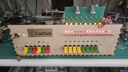
Both the Cactus (the original wooden prototype from years ago) and the new PCB Cactus(es) are essentially derived from a minimal 6502 computer design by Grant Searle for their core logic. Here's what that would look like on a breadboard:
There isn't much to it, it's 32K of RAM, 16K of ROM containing Ohio Scientific's version of Microsoft BASIC, a 6850 ACIA for serial interaction, some logic gates, and of course a 6502 microprocessor (NMOS or CMOS, doesn't matter which). You hook it into a terminal and away you go.
Grant's design in turn can be best described as a distilled, modernized version of the OSI Challenger series of computers. Here's an OSI-400 and a Challenger 4P respectively:

The left one is a replica of the 400 circa 1976, also called the Superboard. It was affordable, endlessly reconfigurable and hackable, but ultimately very limited in capabilities. No BASIC, minimal monitor ROM you talk to over serial, but you could connect it to a bus to augment its features and turn it into a more powerful computer.
Whereas the OSI C4P on the right from about 1979 has more RAM, a video card, keyboard, BASIC built in, serial interface, cassette tape storage, and that's just the standard configuration. There was more room to expand and augment it to your needs inside the chassis (alot changed in 3 years for home computer users).
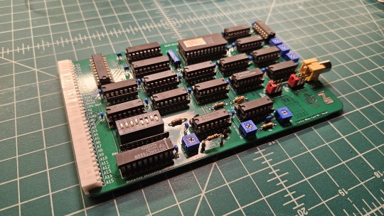
Grant's minimal 6502 design running OSI BASIC is a good starter project for hobbyists. I learned about the 6502's memory map decoding from his design. I modified and implemented his design on a separate cards that could connect to a larger backplane.
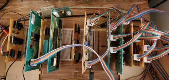
Here are the serial, ROM, RAM, and CPU cards respectively:
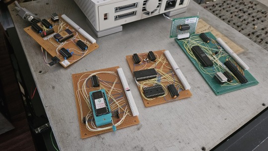
Each one is 100% custom, containing many modifications and fixes as I developed the design. However, that's only half of the computer.
I really wanted a 6502 machine with a front panel. People told me "nobody did that", or couldn't think of examples from the 1970s but that seemed really strange to me. Especially since I had evidence to the contrary in the form of the OSI-300:
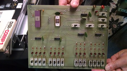
This one I saw at VCF West back in 2018 illustrates just how limited of a design it is. 128 bytes of RAM, no ROM, no serial -- just you, the CPU, and toggle switches and LEDs to learn the CPU. I was inspired the first time I saw one in 2015 at VCF East, which is probably when this whole project got set in motion.
Later that year I bought a kit for a miniature replica OSI-300 made by Christopher Bachman, and learned really quickly how limited the design philosophy for this particular front panel was. It was a major pain in the ass to use (to be clear, that's by OSI's choice, not any fault of Christopher in his implementation)

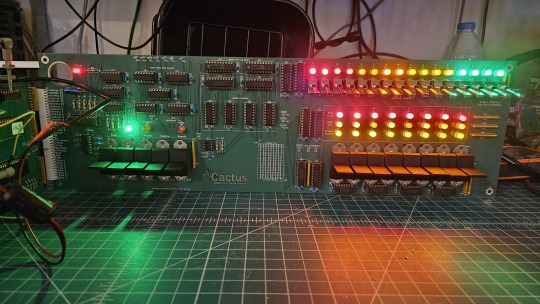
So... I designed my own. Took awhile, but that's the core of what the Cactus is: my attempt at experiencing the 1970s homebrew scene by building the computer I would have wanted at the time. Over half of the logic in the Cactus is just to run the front panel's state machine, so you can examine and modify the contents of memory without bothering the 6502. I added in all of the things I liked from more advanced front panels I had encountered, and designed it to my liking.
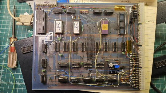
Here's the original front panel, accompanying logic, and backplane connected to the modern single board computer (SBC) version of the machine:
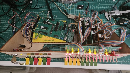
And here's the new Cactus SBC working with the new front panel PCB, which combines the logic, physical switch mountings, and cabling harnesses into a single printed circuit board.
So, what can you do with it? Pretty much the same things I do already with other contemporary 1970s computers: play around in BASIC, fire up the occasional game, and tinker with it.
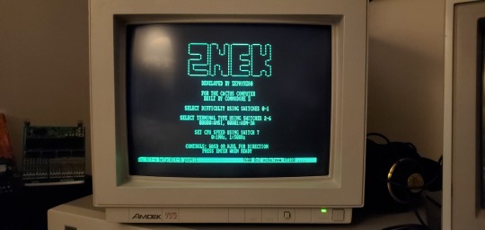
I've got no permanent storage designed for the Cactus as yet, it's been one of those "eventually" things. The good news is that a variety of software can be ported to the hardware without too much trouble for an experienced hobbyist. A friend of mine wrote a game called ZNEK in 6502 assembly which runs from a terminal:
Right now, you have to either toggle in machine programs from the front panel from scratch, burn a custom ROM, or connect it to a serial terminal to gain access to its more advanced features:

Here's it booted into OSI BASIC, but I have also added in a modern descendant of Steve Wozniak's WOZMON software for when I need to do lower level debugging.
I've also got a video card now, based on the OSI-440. I have yet to implement a keyboard, or modify BASIC to use the video board instead of the serial connection. Even if I did, screen resolution is pretty limited at 24x24 characters on screen at once. Still, I'm working on that...

Anyway, I hope that answers your question. Check the tags below to see the whole process stretching back to 2017 if you're curious to learn more of the project's history. I'm also happy to answer any more questions you might have about the project.
267 notes
·
View notes
Text
Hell is terms like ASIC, FPGA, and PPU
I haven't been doing any public updates on this for a bit, but I am still working on this bizarre rabbit hole quest of designing my own (probably) 16-bit game console. The controller is maybe done now, on a design level. Like I have parts for everything sourced and a layout for the internal PCB. I don't have a fully tested working prototype yet because I am in the middle of a huge financial crisis and don't have the cash laying around to send out to have boards printed and start rapidly iterating design on the 3D printed bits (housing the scroll wheel is going to be a little tricky). I should really spend my creative energy focusing on software development for a nice little demo ROM (or like, short term projects to earn money I desperately need) but my brain's kinda stuck in circuitry gear so I'm thinking more about what's going into the actual console itself. This may get techie.
So... in the broadest sense, and I think I've mentioned this before, I want to make this a 16-bit system (which is a term with a pretty murky definition), maybe 32-bit? And since I'm going to all this trouble I want to give my project here a little something extra the consoles from that era didn't have. And at the same time, I'd like to be able to act as a bridge for the sort of weirdos who are currently actively making new games for those systems to start working on this, on a level of "if you would do this on this console with this code, here's how you would do it on mine." This makes for a hell of a lot of research on my end, but trust me, it gets worse!
So let's talk about the main strengths of the 2D game consoles everyone knows and loves. Oh and just now while looking for some visual aids maybe I stumbled across this site, which is actually great as a sort of mid-level overview of all this stuff. Short version though-
The SNES (or Super Famicom) does what it does by way of a combination of really going all in on direct memory access, and particularly having a dedicated setup for doing so between scanlines, coupled with a bunch of dedicated graphical modes specialized for different use cases, and you know, that you can switch between partway through drawing a screen. And of course the feature everyone knows and loves where you can have one polygon and do all sorts of fun things with it.
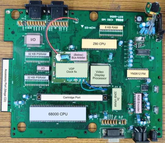
The Genesis (or Megadrive) has an actual proper 16-bit processor instead of this weird upgraded 6502 like the SNES had for a scrapped backwards compatibility plan. It also had this frankly wacky design where they just kinda took the guts out of a Sega Master System and had them off to the side as a segregated system whose only real job is managing the sound chip, one of those good good Yamaha synths with that real distinct sound... oh and they also actually did have a backwards compatibility deal that just kinda used the audio side to emulate an SMS, basically.
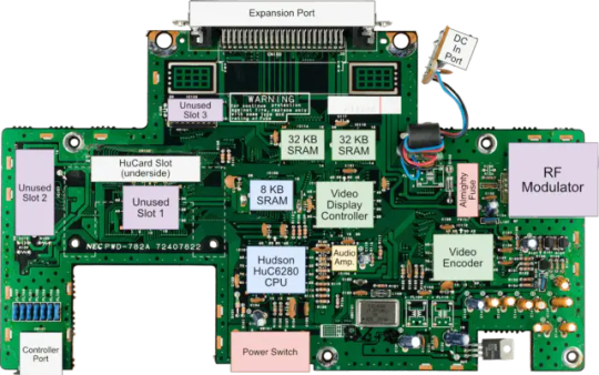
The TurboGrafix-16 (or PC Engine) really just kinda went all-in on making its own custom CPU from scratch which...we'll get to that, and otherwise uh... it had some interesting stuff going on sound wise? I feel like the main thing it had going was getting in on CDs early but I'm not messing with optical drives and they're no longer a really great storage option anyway.
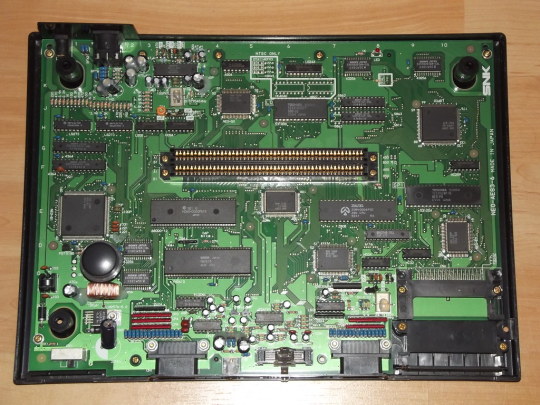
Then there's the Neo Geo... where what's going on under the good is just kind of A LOT. I don't have the same handy analysis ready to go on this one, but my understanding is it didn't really go in for a lot of nice streamlining tricks and just kinda powered through. Like it has no separation of background layers and sprites. It's just all sprites. Shove those raw numbers.
So what's the best of all worlds option here? I'd like to go with one of them nice speedy Motorolla processors. The 68000 the Genesis used is no longer manufactured though. The closest still-in-production equivalent would be the 68SEC000 family. Seems like they go for about $15 a pop, have a full 32-bit bus, low voltage, some support clock speeds like... three times what the Genesis did. It's overkill, but should remove any concerns I have about having a way higher resolution than the systems I'm jumping off from. I can also easily throw in some beefy RAM chips where I need.
I was also planning to just directly replicate the Genesis sound setup, weird as it is, but hit the slight hiccup that the Z80 was JUST discontinued, like a month or two ago. Pretty sure someone already has a clone of it, might use that.
Here's where everything comes to a screeching halt though. While the makers of all these systems were making contracts for custom processors to add a couple extra features in that I should be able to work around by just using newer descendant chips that have that built in, there really just is no off the shelf PPU that I'm aware of. EVERYONE back in the day had some custom ASIC (application-specific integrated circuit) chip made to assemble every frame of video before throwing it at the TV. Especially the SNES, with all its modes changing the logic there and the HDMA getting all up in those mode 7 effects. Which are again, something I definitely want to replicate here.
So one option here is... I design and order my own ASIC chips. I can probably just fit the entire system in one even? This however comes with two big problems. It's pricy. Real pricy. Don't think it's really practical if I'm not ordering in bulk and this is a project I assume has a really niche audience. Also, I mean, if I'm custom ordering a chip, I can't really rationalize having stuff I could cram in there for free sitting outside as separate costly chips, and hell, if it's all gonna be in one package I'm no longer making this an educational electronics kit/console, so I may as well just emulate the whole thing on like a raspberry pi for a tenth of the cost or something.
The other option is... I commit to even more work, and find a way to reverse engineer all the functionality I want out with some big array of custom ROMs and placeholder RAM and just kinda have my own multi-chip homebrew co-processors? Still PROBABLY cheaper than the ASIC solution and I guess not really making more research work for myself. It's just going to make for a bigger/more crowded motherboard or something.
Oh and I'm now looking at a 5V processor and making controllers compatible with a 10V system so I need to double check that all the components in those don't really care that much and maybe adjust things.
And then there's also FPGAs (field programmable gate arrays). Even more expensive than an ASIC, but the advantage is it's sort of a chip emulator and you can reflash it with something else. So if you're specifically in the MiSTer scene, I just host a file somewhere and you make the one you already have pretend to be this system. So... good news for those people but I still need to actually build something here.
So... yeah that's where all this stands right now. I admit I'm in way way over my head, but I should get somewhere eventually?
11 notes
·
View notes
Text
AC PCB Repairing Training Institute
AC PCB Repairing Training Institute: Skill Development
With the increasing demand for ventilation in homes, offices, and workplaces, maintenance planning and maintenance are essential.AC PCB Repairing Training Institute The most important part of an AC system is the circuit board or PCB, which controls the operation of the AC system. Teaching is a great profession where you have to study and get good grades. That’s where the AC PCB Knee Repair Academy comes into play.

Why choose AC PCB Repairing Training Institute?
Enrollment in a professional training school offers the person structured, practical training that cannot be obtained by self-study.AC PCB Repairing Training Institute Professional training teaches students technical skills in AC PCB systems, provides them with practical sessions, and prepares them for actual repair situations. Training schools also give students up-to-date information on the latest trends and tools utilized in the trade.
Major Benefits of Training
An efficiently structured training course covering theoretical and practical topics of PCB repairing.
Practical training in equipment and techniques used in the electronics repairing business
Practice exposure in actual AC PCB faults under the guidance of experienced trainers.
Certification to improve trainees' credibility and marketability.
Training in safety procedures, customer service, and service reporting.
Course Content and Learning Outcomes
A successful AC PCB Repairing Course includes the following:
Introduction to AC components and their uses
PCB design and layout concepts
Understanding the working principle of air conditioners
Decision and diagnosis of common faults in AC PCB
Soldering and desoldering techniques
Use of measurement devices such as multimeters and oscilloscopes
Step by step process of repairing and replacing faulty components
Precautions while repairing
Upon successful completion of this course, students can repair and diagnose various types of AC PCB-related faults independently.
Who should take the course?
This course is suitable for all types of individuals, such as:
School passouts or ITI students interested in technical and job-fit skills
Technicians and electricians who want to offer extension services
Those interested to start small AC or electronics repair shop businesses
Hobbyists interested in repairing circuits and electronics
The course is able to handle fresh entrants with no technical background as well as experienced candidates with experience in electronics.
Choosing the Right Training Institute
While choosing an AC PCB Repairing Training Institute, the following should be kept in mind:
A well-designed syllabus with theory and practical training
Trained faculty with hands-on industry experience
Availability of recent tools and test equipment for training
Good ratings and feedback by students
Employer- and service center-approved certification
Job placement facilities or internship exposure
Choosing a local institute can also provide greater convenience and accessibility.
Career Opportunities After Course Completion
Completing a professional course in AC PCB Repairing makes one conscious of numerous job opportunities, such as:
AC repair specialist with specialized PCB services
Brand service center air conditioner engineer
Independent PCB repair specialist
Home AC repairing and maintaining business owner
Technical support experts in appliance companies
After experience and training, a person can be a good professional in a growing field.
Last Words
Professional training facility AC PCB Repairing Training Institute is a smart investment for any individual who desires to start an electronics repair business. It not only provides real, job-oriented skills but also introduces opportunities for self-employment and professional growth. Choosing an appropriate training facility ensures that you are getting quality training, proper certification, and guidance to be successful in the business.
Begin your career path today by joining a reliable AC PCB Repairing Training Institute and become proficient and confident enough to be a professional electronics repair technician.
2 notes
·
View notes
Text

Multilayer PCBs offer enhanced functionality by incorporating multiple circuit layers into a single board. These versatile boards enable complex electronic designs, compact layouts, and signal integrity. Our multilayer PCBs are meticulously manufactured, meeting industry standards for various applications, including consumer electronics, telecommunications, and aerospace technology.
Visit: https://sqpcb.com/products_category/multilayer-pcb
#Multilayer PCB#customized pcb boards#customize pcb#pcb board#aluminium pcb board#pcb china#printed circuit board#aluminum base pcb#circuit board#custom circuit boards
0 notes
Text
Unlocking Innovation in Electronics: The Power of Specialized PCBs
In the world of modern electronics, printed circuit boards (PCBs) serve as the essential foundation of nearly every device, from consumer gadgets to advanced industrial systems. As technology continues to evolve, the demand for highly specialized PCBs such as blind via PCBs, ceramic PCBs, flex PCBs, copper based PCBs, and custom PCB boards has surged dramatically. These innovations not only provide enhanced performance but also meet the increasing complexity of today’s electronic applications.
In this article, we’ll explore the key types of advanced PCBs, including the benefits of working with a reliable blind vias PCB manufacturer, the importance of custom PCB manufacturers, and how these different PCB types are shaping the future of electronic product design.
What Are Blind Via PCBs?
One of the most significant advancements in PCB design is the blind via PCB. Vias are the holes that connect different layers of a multi-layer PCB. In blind vias printed circuit boards, these holes connect an outer layer to one or more inner layers without penetrating the entire board. This feature allows for a more compact and efficient layout, especially in high-density interconnect (HDI) applications.
By incorporating blind vias, engineers can increase component density without sacrificing board size or performance. This makes blind via PCBs ideal for applications such as smartphones, medical devices, and compact industrial electronics where space is at a premium.
A reputable blind vias PCB manufacturer uses laser drilling or advanced mechanical drilling to achieve precise and clean vias, ensuring optimal performance and reliability. These manufacturers often provide design support to ensure that the via placement aligns with the functional needs of the product while maintaining cost efficiency.
Ceramic PCBs: High Thermal Conductivity for Harsh Environments
Another innovative PCB solution is the ceramic PCB, which is particularly suited for high-power or high-frequency applications. These boards are made using ceramic substrates like aluminum oxide (Al2O3) or aluminum nitride (AlN), which offer excellent thermal conductivity and mechanical stability.
Ceramic PCBs are widely used in LED lighting, automotive electronics, and aerospace systems, where conventional PCBs might fail due to heat or mechanical stress. Their ability to operate in extreme conditions while maintaining electrical performance sets them apart from traditional boards.
Choosing a knowledgeable ceramic PCB manufacturer is crucial. Such manufacturers specialize in using thick film or direct bond copper (DBC) technology to create boards that can handle high temperatures and thermal cycling without degradation. Their manufacturing processes are tailored to ensure the structural integrity and thermal performance required by demanding industries.
Copper Based PCBs: Power and Durability Combined
Copper based PCBs are designed for applications where heat dissipation and current carrying capacity are critical. These boards use a thick copper layer—typically 1 oz to 10 oz per square foot—making them ideal for power supplies, automotive systems, and industrial control equipment.
The thick copper not only supports high current loads but also aids in effective heat dissipation, which extends the lifespan of both the board and its components. In power electronics, copper based PCBs are often the go-to choice due to their durability and performance.
Whether it’s single-layer or multi-layer copper boards, selecting a manufacturer with experience in copper based PCB production ensures precision in etching and lamination processes, which are crucial for maintaining electrical efficiency.
Flex PCBs: The Future of Flexible Electronics
As electronic devices become more compact and ergonomic, flex PCBs (flexible printed circuit boards) are gaining popularity. These boards are made from flexible substrates like polyimide, which allow them to bend and twist without breaking.
Flex PCBs are used in wearable technology, medical devices, and compact consumer electronics. Their unique design makes it possible to connect electronic components in tight or irregular spaces, something rigid PCBs cannot accommodate.
Unlike traditional boards, flex PCBs require special expertise in both design and manufacturing. A skilled flex circuit manufacturer will take into account factors like bending radius, dynamic flexing requirements, and signal integrity to deliver a board that performs reliably under mechanical stress.
The Importance of Custom PCB Boards
While standardized PCBs serve many applications, unique projects often require custom PCB boards designed to meet specific electrical, mechanical, or thermal requirements. A custom PCB could involve specific layout constraints, unusual form factors, or integration with other technologies like sensors or embedded antennas.
Working with an experienced custom PCB manufacturer provides access to tailored design, prototyping, and production services. Whether it’s a custom PCB board for a wearable fitness tracker or a complex multi-layer design for a satellite module, the ability to customize every aspect of the board’s structure is a key advantage in competitive industries.
Customization also enables designers to optimize the board for size, performance, and cost—something that off-the-shelf PCBs cannot provide. A good custom PCB manufacturer will work closely with engineers to understand application needs and deliver a solution that meets both technical and budgetary goals.
Choosing the Right PCB Manufacturer
With so many specialized PCB types available, it’s essential to partner with a manufacturer that offers comprehensive capabilities. Whether you’re sourcing a blind vias PCB manufacturer, a ceramic PCB manufacturer, or a supplier of flex PCB and copper based PCB solutions, the ideal partner will offer:
Advanced manufacturing technologies
In-house engineering support
Quick turnaround and low minimum order quantities
Certifications such as ISO and UL
Quality assurance testing at every stage
Partnering with a one-stop manufacturer that offers everything from custom PCB design to assembly and testing ensures a smoother production process and a higher-quality final product.
Conclusion
The electronics industry continues to push boundaries, demanding more compact, efficient, and robust solutions. From blind via PCBs that enhance space utilization, to ceramic PCBs built for harsh environments, and flex PCBs that enable groundbreaking product designs, the world of PCB manufacturing is more dynamic than ever.
Whether you're designing a next-generation wearable, an industrial automation controller, or a high-power automotive system, choosing the right type of PCB—and the right manufacturer—is crucial. Work with a proven custom PCB manufacturer that understands your needs, offers flexible solutions, and delivers on time and within budget.
By leveraging specialized boards such as blind vias printed circuit boards, ceramic PCBs, and copper based PCBs, you’re not just building a device—you’re building a competitive advantage.
0 notes
Text

“J K Enterprises” is a reputed Sole Proprietorship (Individual) firm, registered in the year 2015. We are engaged in Manufacturing a diverse range of REFRESH PCB Board, Laptop Charger, Mobile Chargers, USB Chargers, Mobile Adapter, Data Cable etc. These products are manufactured in our high-tech manufacturing unit using supreme grade raw material. With the core values of transparency and uprightness, we are building a collaborative platform for ourselves in the market. Our company is facilitated with all kinds of requisites for qualitative production.
Under the proficient management of our mentor, Mr. JUNAID KHAN, we have earned an unrivaled position in the market and gained massive acceptance of our esteemed customers. Our company is based on the grounds of moral values, principles, and ethics which are led by our mentor.
2 notes
·
View notes
Text
Essential Tips for Efficient Two-Layer PCB Stencil
Please discover essential tips for achieving maximum efficiency with two-layer PCB stencils. From accurate alignment and stencil thickness selection to the right solder paste application techniques, this guide covers everything you need to know for precise, high-quality, two-layer PCB assembly.

#PCB manufacturer#PCB fabrication In india#custom PCB manufacturing in india#prototype PCB manufacturing#low-cost PCB manufacturer#high-quality PCB manufacturing#quick turn PCB fabrication#flex PCB manufacturer#multilayer PCB manufacturer#Best pcb manufacturer#Top 10 pcb manufacturer#Pcb manufacturer near me#Pcb manufacturer in Maharashtra#Pcb manufacturer in haryana#Pcb manufacturer in delhi#Pcb manufacturer in india#Pcb manufacturer in Bombay#Pcb manufacturer in jaipur#Best pcb assemble in hyderabad#Low cost pcb assembled in hyderabad#Good pcb assemble in hyderabad#Free sample pcb assemble in India#pcb stencils#Two layer pcb stencil#Best pcb stencil maker in hyderabad#SMD pcb board assembly in hyderabad#Multi Color Pcb#Sharp Legends
0 notes
Text
PCB Fabrication is the foundational process that transforms raw materials into the physical structure of a Printed Circuit Board. It involves several steps that convert a schematic diagram into a tangible board. This process lays down the framework for the electronic components that will be added later.
0 notes
Video
youtube
FPC flexible circuit board production process #fpc #circuitboard #pcb #technology #factory #customer #icgoodfind
2 notes
·
View notes