#I2C Level Converter
Explore tagged Tumblr posts
Visit Tumblr Blog
Explore Tumblr blogs with no restrictions, modern design and the best experience.
Last Seen Tumblr Blogs


Fun Fact
Tumblr’s website traffic is steadily declining.
Text
https://www.futureelectronics.com/p/semiconductors--comm-products--i2c/pca9515adp-118-nxp-5973557
I2C CAN Bus Module, I2C adapter, I2C devices, Serial Peripheral Interface
PCA9515A Series 3.6 V 5 mA 400 kHz 6 pF Surface Mount I2C-bus Repeater - SOIC-8
#Comm Products I2C#PCA9515ADP#118#NXP#I2C CAN Bus Module#I2C adapter#I2C devices#Serial Peripheral Interface#I2C Level Converter#i2c protocol#spi protocol#uart protocol#i2c communication#i2c protocol in embedded system#I2C-bus Repeater
1 note
·
View note
Text
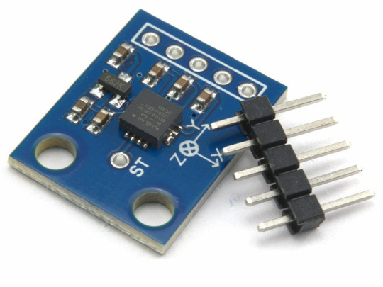
GY-511 module includes a 3-axis accelerometer and a 3-axis magnetometer. This sensor can measure the linear acceleration at full scales of ± 2 g / ± 4 g / ± 8 g / ± 16 g and magnetic fields at full scales of ± 1.3 / ± 1.9 / ± 2.5 / ± 4.0 / ± 4.7 / ± 5.6 / ± 8.1 Gauss. When you place this module in a magnetic field, according to the Lorentz law, a current is induced in its microscopic coil. The compass module converts this current to the differential voltage for each coordinate direction by calculating these voltages, you can calculate the magnetic field in each direction and obtain the geographic position. It communicates using I2C communication protocol and the voltage level required to power this device is 3V-5V. You can use it in DIY GPS system, accelerometer data acquisition system to be used in Vehicles etc.
3 notes
·
View notes
Text
USB RTC for Raspberry Pi: The Best Way to Enhance Your Raspberry Pi's Time Accuracy

When it comes to building real-time applications with the Raspberry Pi, one of the most crucial components to ensure is timekeeping. A RTC (Real Time Clock) module provides the Raspberry Pi with a reliable source of time, even when the system is powered off. For those looking to achieve incredibly accurate timekeeping, a USB RTC for Raspberry Pi is a solution that combines the DS3231 RTC chip with a MCP2221 USB to I2C/UART converter is a perfect match.
In this blog post, we'll dive deep into what makes this USB RTC setup an ideal choice for your Raspberry Pi projects, and how it enhances accuracy, reliability, and ease of use.
What is USB RTC?
RTC is a device which is used for maintaining accurate time in the host’s system processor. With the Raspberry Pi, the internal clock relies on the system supply to track the accurate time and the main issue is when the Raspberry Pi is powered off, the clock resets. USB RTC is a solution for providing accurate timekeeping even when the Raspberry Pi is turned off or disconnected from the network. This setup allows users to easily add accurate timekeeping to their Raspberry Pi without using the GPIO pins.
The USB RTC is a device which comes with a strongly integrated DS3231 circuit that is used to consume less power and has an integrated temperature-compensated crystal oscillator. It has MCP2221, a USB-to-UART/I2C serial converter that provides USB connectivity, used in Raspberry Pi operations that contain USB, UART(Serial), GPIO, and I2C interfaces. This module can be used with Raspberry Pi, Windows, Linux or any other operating system.
Key Features & Specifications:
DS3231 RTC Circuit: The DS3231 provides a highly stable timekeeping function and includes a built-in temperature-compensated crystal oscillator (TCXO), which helps maintain accuracy across a wide temperature range.
Temperature-Compensated Crystal Oscillator (TCXO): This is a critical feature of the DS3231. TCXO compensates for temperature variations that could affect timekeeping accuracy. This ensures the RTC module performs well in a range of environments without the need for external temperature sensors.
Battery Backup (CR1220, 3V): The module uses a CR1220 coin-cell battery to maintain time even when the Raspberry Pi is powered off. This ensures your system's time is preserved even in the event of power failure or system reboot.
16-pin, 300-mil SO Package: The module comes in a compact and durable 16-pin, 300-mil SO (Small Outline) package. This size makes it easy to integrate into your projects.
Automated Backup Power Supply: The onboard battery backup power supply ensures your RTC chip continues to run and track time even when the Raspberry Pi is turned off or disconnected from power.
Fast 400kHz I2C Interface: The RTC communicates with the Raspberry Pi using a 400kHz I2C interface, allowing fast and efficient data transfer. This is crucial for time-sensitive applications, as it minimizes any lag or delay when reading the time or setting the RTC.
MCP2221 USB to I2C/UART Converter: The MCP2221 is a USB-to-I2C and UART converter that makes it easy to connect the RTC to the Raspberry Pi via a USB port. This eliminates the need for GPIO pins, making it a plug-and-play solution for Raspberry Pi users.
USB 2.0 Compatibility: The module uses USB 2.0 for a fast and stable connection to the Raspberry Pi, offering plug-and-play functionality without requiring complicated wiring or software configuration.
Plug-and-play: The device is plug-and-play, with available drivers for various operating systems, including Linux, ensuring smooth integration with the Raspberry Pi.
High Accuracy: ±2ppm from 0°C to +40°C: Offers incredible timekeeping accuracy of ±2ppm (parts per million) between 0°C and +40°C. This means that, in a typical environment, the RTC will deviate by no more than 2 seconds per day—a level of precision ideal for most hobbyist and professional projects.
Extended Accuracy Range: ±3.5ppm from -40°C to +85°C: In more extreme conditions, such as outdoor or industrial applications, this module maintains an accuracy of ±3.5ppm in the temperature range of -40°C to +85°C. Whether you're working in a chilly warehouse or a hot outdoor environment, this module ensures your Raspberry Pi’s timekeeping remains precise.
Versatile Timekeeping: The module doesn’t just count seconds and minutes; it also tracks days, dates, months, and even the year with leap year compensation valid until the year 2100. This makes it perfect for long-term projects, as you can rely on the RTC to keep accurate time for many years to come.
Two Time-of-Day Alarms: With two independently programmable time-of-day alarms, this RTC module allows you to set scheduled events. Whether you need to trigger an action, send a notification, or turn on/off a device at specific times, the alarms make it easy to synchronize with your Raspberry Pi’s actions.
Programmable Square-Wave Output: The square-wave output feature allows you to generate periodic signals that can be used to sync other devices. Especially useful in projects that require precise timing for communications or measurements.
Use Cases:
Data logging: For applications like weather stations or scientific experiments, you need precise timestamps for each data point.
Embedded systems: For embedded systems that require time-based tasks (like alarms or scheduled events), the RTC ensures that the system runs on a stable, reliable time.
Low-power applications: The RTC ensures your Raspberry Pi can operate in low-power or battery-operated setups while maintaining the correct time.
IoT devices: When building IoT applications where devices may not always have a constant internet connection, having a local, accurate time source is essential.
Conclusion:
For projects that demand extremely accurate timekeeping, the combination of the DS3231 RTC chip and the MCP2221 USB to I2C/UART converter is an excellent solution. This setup not only provides highly accurate, temperature-compensated time tracking but also integrates seamlessly with the Raspberry Pi via a fast I2C interface.
Whether you're building a weather station, data logger, or any time-sensitive project, the DS3231 with MCP2221 ensures that your Raspberry Pi has reliable, battery-backed, and accurate timekeeping capabilities that won't be affected by power outages or system restarts.
#technology#rtc#innovation#tech#iot#raspberry pi#projects#iot applications#iotsolutions#usb rtc#real time projects
0 notes
Text
ADXL335 Module
The ADXL335 Module is a compact and energy-efficient 3-axis accelerometer that provides signal conditioned voltage outputs. ADXL335 Module has a minimum full-scale range of ±3 g for accurately measuring acceleration.
This breakout board has the capability to measure both static gravity acceleration in tilt-sensing scenarios, as well as dynamic acceleration caused by movement, impact, or tremors. It is equipped with a built-in voltage regulator and operates seamlessly at 3.3V and 5V (3-5V).
An accelerometer is an electro-mechanical device capable of measuring both static and dynamic acceleration forces. This includes the constant force of gravity acting on your feet, as well as any movement or vibrations that may affect the device.
Systems such as FPV, RC, and Robots.
Navigation systems that utilize GPS technology
Acknowledging and recording the effects.
Devices used for gaming and virtual reality experiences
Features that are activated by movement.
Efficient energy conservation for portable devices.
Monitoring and compensating for vibrations
The detection of free-fall.
Detecting 6D orientation
The characteristics include:
One feature on the board is a Low Dropout (LDO) Voltage Regulator.
Can be connected to either a 3V3 or 5V Microcontroller.
With an ultra-low power consumption rate of only 40uA in measurement mode and an impressive 0.1uA in standby at 2.5V, this device ensures efficiency without compromising on performance.
This feature includes the ability to detect taps and double taps.
A feature for detecting free-fall is included.
The analog output has been successfully connected to the device and is now functioning properly.
Incorporate an ultra low noise linear LDO voltage regulator.
The device contains built-in onboard filters that effectively minimize noise from the motor and other high current electronics.
All sensors on the I2C bus
By using a soldered jumper, it is simple to choose two I2C addresses for the MPU6050.
The LED indicating power.
Incorporate a Logic level converter for I2C connectivity.
Optimized for 5V logic
1 note
·
View note
Text
What is power management ic?
A power management IC is an integrated circuit or a group of ICs responsible for the conversion, distribution, detection, and other power management of electrical energy in electronic equipment systems. It is mainly responsible for converting source voltage and current into power that can be used by loads such as microprocessors and sensors. It is designed to manage and control electronic devices' power supply and power consumption.
PMICs are commonly used in various applications, including smartphones, tablets, laptops, IoT devices, embedded systems, and more. They are vital in optimizing power efficiency, extending battery life, and ensuring stable and reliable power delivery to various components within a device.
Key functions and features of power management ICs may include:
Voltage Regulation: PMICs typically include voltage regulators that convert an input voltage to the output voltage levels required by different components within the device.

Power Sequencing: PMICs can control the sequence in which various power rails are turned on or off to ensure proper device startup and shutdown sequencing.
Battery charging: Many PMICs contain battery charging circuitry that manages the charging process, including monitoring battery status, adjusting charging current, and preventing overcharging or over-discharging.
Power Monitoring: PMICs can provide information about power consumption, voltage, and current levels, which is useful for system monitoring and optimization.
Thermal Management: Some PMICs have features that monitor and control the device's temperature to prevent overheating and ensure safe operation.
Power efficiency: PMICs often employ voltage regulation and power gating techniques to maximize power efficiency and extend battery life.
Fault protection may include various protection mechanisms against overvoltage, overcurrent, and short-circuit conditions.
Load Switch: PMICs can control the turn on/off status of specific components or peripherals to save power when not in use.
Power saving modes: They can provide different power saving modes such as sleep, standby, and low-power modes to reduce power consumption during idle periods.
Communication interfaces: PMICs can communicate with the device's main processor or microcontroller through interfaces such as I2C, SPI, or UART, allowing dynamic power management based on system needs.
The specific features and functionality of a PMIC may vary depending on the application and requirements of the electronic device. By efficiently managing power, PMICs help extend battery life, improve performance, and improve reliability in portable and battery-powered devices.
You May Also Like:What Is a Hexa Core Processor?
What happens if the power IC is damaged?
If a Power Management IC (PMIC) in an electronic device is damaged, it can have a range of negative consequences, depending on the extent of the damage and the specific functions of the PMIC. Here are some potential outcomes and issues that can occur if the PMIC is damaged:
Power Supply Issues: The most immediate and significant impact of a damaged PMIC is disruptions in power supply. The device may experience voltage instability, leading to erratic behavior or complete failure. Components receiving incorrect voltage levels may not function correctly or could be damaged.
Device Failure: In many cases, a damaged PMIC can lead to the failure of the entire electronic device. This is especially true if the PMIC regulates critical power rails or manages battery charging.
Battery-Related Problems: If the PMIC is responsible for battery management, a damaged PMIC can lead to issues with the device's battery. This might include overcharging, over-discharging, or failing to charge the battery. Battery-related problems can result in reduced battery life or even battery damage.

Reduced Power Efficiency: A damaged PMIC may not be able to perform power optimization functions effectively. This can increase power consumption, reduce battery life, and decrease overall device efficiency.
Overheating: If the PMIC is responsible for thermal management, a damaged IC might not be able to properly regulate the device's temperature. This can lead to overheating, which can, in turn, cause further damage to the device's components.
Inconsistent Behavior: Devices with damaged PMICs may exhibit inconsistent behavior. They might power on and off randomly, freeze, or become unresponsive. These issues can make the device unreliable or unusable.
Safety Risks: Depending on the nature of the damage, a malfunctioning PMIC can pose safety risks. For example, if it fails to regulate power correctly, it might expose components to voltage levels they are not designed to handle, potentially causing electrical shorts or fires.
You May Need to Know: TPS61096ADSSR RT9065GE SGM2019-2.7YN5G SY8303AIC
Loss of Data: A damaged PMIC can sometimes lead to data loss or corruption if the device crashes or shuts down unexpectedly.
Difficulty in Diagnosis and Repair: Troubleshooting and repairing a device with a damaged PMIC can be challenging. Identifying the PMIC as the root cause of issues may require specialized tools and expertise.
In summary, a damaged Power Management IC can have a wide range of adverse effects on an electronic device, from causing immediate failure to leading to issues with power supply, battery management, and overall device functionality. Repairing or replacing a damaged PMIC often requires skilled technicians and may involve replacing the IC itself or the entire motherboard, depending on the device's design and the extent of the damage.
0 notes
Text

I have this delusion that if I can make real life Doc Ock arms she'll become real and love me. So I'm gonna try and do that before I get bored and it becomes another discarded folder of CAD on my desktop.
I'm going to use electromagnets to do it, because that's one of the only ways I could think of trying to replicate the soft robotic arms from Spiderverse. (I know that's not how actual soft robotics work, but I just have a 3d printer so I'm working with what I've got) I'm starting off with a proof of concept, basically just taking an electromagnet, putting it at one end of a shell with some metal on the other end and seeing if I can compress and extend it.

I made an electromagnet calculator to get the dimensions and power requirements needed for the force I want. I originally wanted to get 100N at 75mm gap between top and bottom but that would either require a way beefier power supply or really large coils, so I reduced my expectations. I have some DC motor drivers ordered to actually run the coils and I have a old laptop power supply combined with a buck converter to drop the voltage to the correct level.


For the physical design I went with two half circles intersecting, this was to hopefully make it bend near the middle instead of the ends. I've run some basic FEA on it, but I don't have the material properties for TPU so it mostly just helped to beef up the areas near the threads to prevent them from buckling rather than getting a good simulation of how it will fold. Once I get the magnets working I'll play around with some more exotic shapes to see what works the best. I might even try adjusting the wall thickness through the height.
I just realized that I need to actually find a way to secure the spools to the little caps because right now they're just indexed with the nubs. I thought about super gluing them but I do want to be able to retrieve them at some point for use in future versions.
To actually test them I'm going to hook them up to an Arduino Nano or something with the motor drivers. To actually test how much force they're outputting I though about using a kitchen scale and seeing that way. Another though was to just get a 2kg weight and put it on it. That way if it can lift that up it fulfills the requirements I set up (20N at 75mm gap between magnet and metal). I've also though about making some sort of jig with a load cell. It would let me get more precise data but means I spend time designing and manufacturing more testing infrastructure rather than the actual project.

If I am going to be making more coils, then I might need to think about making a jig or machine for winding them. My calcs say I need coils with a couple hundred turns at least, so making a simple machine to turn them for me would save a lot of time if I want to make a lot of nodules. The main issues I see are getting
If the tests works then I'll move onto a version with four sets of magnets so I can bend the nodule (I'm calling them nodules) in any direction. I'd also like to get some PCBs for controlling them, that way I can connect them up to each other a main hub through I2C or something and collect data like temp. I also have to think about power dissipation because they could sink a good number of Watts, so if I do something funky, like have cut outs for airflow in the PCBs, then have fan at the end of the limb to push air through it could solve that. This is all way in the future though. I need to wait for all the stuff to come in and actually test it.
#doc ock#spiderverse#olivia octavius#otto octavius#engineering#project#3dprinting#mechanical engineering#doctor octopus
19 notes
·
View notes
Text
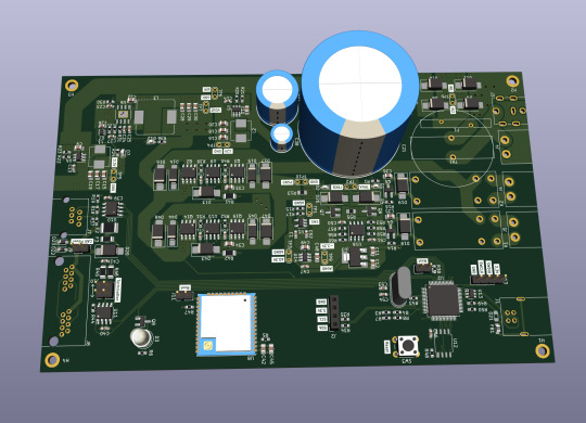
Let me introduce my current main WIP. It's not fandom related, it's for my model railroad, and it's not yet finished.
This is a rendering of a circuit board that I'm designing at the moment. It will be a DCC command station. My model railroad is run digitally, which means the tracks carry digital signals that tell each locomotive and switch individually how to run, which lights to turn and so on. The command station is the device that generates that. I have a number of different layouts, one of which has a good command station, one of which has a crappy old one, and the final one isn't even digital yet. So this will be the one that solves all issues for me, hopefully.
The design above isn't finished yet, and even the parts that are are not yet fully representative. The different capacitors are just there as options; some screen print overlaps; and some components (in particular all plugs and the relays that control the programming track) don't have 3D models so they don't show up.
Planned features:
Four layer board
10-25 V DC output, software controllable
Up to 5A output power, limited mainly by the main switching regulator.
Input 15-25V either AC or DC with polarity protection, selectable with some solder bridges (not yet in there). Optionally you can also bypass the main power regulator with another solder bridge (that I haven't added yet); useful in case you use e.g. a laptop power supply with a switchable voltage and don't need any regulation after that.
Railcom support
USB connection; not yet sure what for, but the main chip I'm using has USB support and I have some spare USB connectors here, so in it goes.
Speaking: The chip is an STM32L433RCT6P, chosen because I found it in stock at an electronics distributor. 64 kB RAM, 256 kB EEPROM, with support for an additional up to 256 MB externally (there's a spot for that on the board) and lots of fun extras that I don't technically need. It has an FPU! I don't need an FPU, but I will definitely do some floating point math computation on it just for fun.
Main external connection is WLAN using an ESP32 WROOM U module. I haven't decided on the housing, but I may go for extruded aluminum, so it's the U version that allows and requires an external antenna
It supports XBUS/XpressNet connections for old throttles from Lenz and Roco that I should probably throw away, but I paid good money for them, dang it.
It supports CAN for LCC / OpenLCB. I may not populate this part on all boards that I'm building, because I haven't actually decided whether I am interested. But the chip has CAN functionality built in, so why not.
There's an I2C connection to connect a cheap tiny OLED display for status messages.
Test points for all important signals (in particular the different internal voltage levels; yes, there is 3.3V, A3.3V and -3.3V and I need all of them).
Stuff still to add:
I will add pin headers (or space for pin headers anyway) for all the remaining pins on the STM32, and perhaps some on the ESP32, for future expansions.
Status LED and stop/go button on the front
Wire it all up, maybe move some stuff (mostly the STM32 around), which will cause all sorts of fun new routing issues.
Adjustments to make the jacks line up with the front panel once I've decided on a housing.
Features I'm not considering adding:
s88. I vaguely know what it is but I don't have any devices like that, and if that ever changed I could probably build (or perhaps buy) a converter that connects them via CAN.
Other buses like LocoNet.
Ethernet. I don't need it and it's actually more expensive than WLAN in this day and age.
In terms of software, I'm planning to use DCC-Ex on it. The whole project actually started out as a DCC-Ex shield, but once I realised that this wouldn't fit, I decided to make it standalone. Now, DCC-Ex is designed for Arduino, not STM32, and it doesn't support XpressNet, nor OpenLCB, nor Railcom, and their Wifi protocol is pretty weird and annoying which will be an issue (I'm planning to write my own control app for iPhone for it), so I'll probably change that or just replace it with the z21 one… so really, the software will not look a lot like DCC-Ex once I'm done with it.
Will this all work? I have honestly no idea. I mean, I'm fairly confident, I'd have given up on this long ago otherwise, but I have no guarantees either way until I've spent a lot of money on components and circuit boards and start soldering. Turns out doing it this way is not really cheaper than just buying a half-way decent one. That's what makes it exciting, though!
If it does work, obviously this will be released as open source. But it's still going to be a few days (more realistically weeks) before it's even ready to order the parts, and then a lot of soldering (current BOM stands at 194 actual components), and then a lot of software development before it's ready for that.
5 notes
·
View notes
Photo

The Absolute Guide to Know Embedded Systems Design
Introduction to Embedded Systems
An embedded system is a digital device whose core component performs computational tasks designed for unique and restrained functionality, and it is applied as an element of the electrical or mechanical system. Such systems need to be reserved for large collections of mechanical and electrical factors that are built into practical units. Embedded, in simple terms, refers to any system within another system.
Embedded System- a Flagship Component for Computation
An embedded system is necessary to perform computational tasks assisted by a microcontroller or a microprocessor. However, the embedded system should be either a microprocessor or a digital signal processor. The embedded system programmer is required to have a detailed understanding of the following terms:
Writing Code
Configuring Peripherals
Testing Code
Refining Code
Debugging Code
Verifying Code
Writing code
C language is considered as the best fit for the embedded system programming because it bridges the gap between high-level software and hardware. Thus, the proficiency of language is important for embedded system programmers.
Configuring peripherals
Many embedded structures will include the use of peripherals such as analog-to-digital converters, programmable counter modules, I2C interfaces, or USB controllers. Embedded designers must consider a variety of factors such as:
● how the peripherals work
● how the peripherals are usually implemented
Testing code
Testing code doesn't imply powering up a system and observing it for a while to verify that it works. The quality analyst must test the embedded system software to identify the defects in the programming in order to improve the performance of an embedded system.
Refining code
The embedded system programmer is required to use the solid refinement methodology to easily implement the modifications in the code and detect & solve bugs during the refinement.
Debugging code
Debugging is quite an indistinct term as it is used to describe the method of discovering and correcting refined errors in code that is less functional. Debugging is an essential element for embedded system development which comes from experience and observation of the skilled embedded designers.
Verifying code
At this point, embedded system designers shall make sure that the code effectively performs the required functions and doesn't capture hearth when something surprising takes place somewhere in the device or the surrounding environment. For example, in the langur test, you provide non-stop input data to the code and affirm that the system doesn't glitch.
Characteristics of Embedded Systems
● Task-Specific: All embedded systems are designed to be task-specific as they do the corresponding task repeatedly over their existence.
● Time-specific: The embedded systems are designed to perform the task within a specific time. Therefore they must perform actively.
● Minimal User Interface: The embedded systems have minimal or no user interface. For example, an automated washing machine operates on its own once the program is set and stops once the job is done.
● Responses: Some embedded systems are invented to respond to outside stimuli and act correspondingly.
● High efficiency: Embedded systems are developed to operate with specific efficiency levels as these systems are small in size and can work with limited power.
● High on Reliability: Embedded systems cannot be modified or enhanced by the users. So, they need to stand high on reliability and endurance.
● Highly Stable: Microcontroller or microprocessors are adopted to create embedded systems as they are highly stable for complex computations.
Typically, embedded systems are reactive systems, meaning, it is in continual interaction with its environment and executes at a pace determined by the particular environment.
Advantages
The benefits of Embedded Systems are as follows:
● They are handy for mass production that affects affordable rates per piece
● The structures of embedded systems are surprisingly secure and reliable
● The embedded structures are made for precise tasks
● The embedded structures are small in size and can be carried and transferred almost anywhere
● These embedded structures are fast, and they use much less power
● The embedded structures optimize the use of assets available
● The embedded structures enhance product quality
Limitations
The shortcomings of Embedded Systems are few as follows:
● The embedded structures cannot be changed once configured. Hence, no enhancement or upgradation can be done on the embedded systems, once designed and created.
● The embedded systems are challenging to maintain and it is also difficult to make a back-up of embedded files.
● Troubleshooting is tough for embedded systems.
● Additionally, transferring facts from one machine to another is somewhat hardwired in the case of embedded systems.
Implementation of Embedded Systems
An embedded system can be tested as a separate unit, and it can also be successful in functioning separately as well. However, the embedded design is essential for integration. Designers of embedded structures want to be acquainted with electricity distribution, conversation interfaces, and interconnection methods because these are the types of equipment that we use to successfully integrate a machine into a large system.
For example, let us understand an embedded model for air quality monitoring. The objective of this system is to eliminate the pollutants, both inside as well as outside the house, and make the room ambient. Therefore, the embedded system implementation utilizes gas sensors, optical dust particle sensors, humidity, and temperature sensors for improving air quality. Aimtron combines the use of electrical as well as environmental engineering to meet these requirements.
Conclusion
Embedded design is a fascinating field as it accommodates a pleasant variety of abilities and tasks, together with analog design, firmware development, PCB layout, interface design, and gadget integration. Feel free to share your feedback in the comment, if you have worked on something that you would consider as an embedded system experience.
2 notes
·
View notes
Text
YoungMinds - VLSI System Design and It’s Importance
Full-form of VLSI is Very Large-Scale Integration, is the process of creating an integrated circuits (IC’s) by combining millions or billions of MOS transistors onto a single chip.
VLSI began in the 1970s when MOS integrated circuit (Metal Oxide Semiconductor) chips were developed and then widely adopted, enabling complex semiconductor and telecommunication technologies. The microprocessor and memory chips are VLSI devices.
VLSI is one of the most widely used technologies for microchip processors, integrated circuits (IC) and component designing. It was initially designed to support hundreds of thousands of transistor gates on a microchip which, as of 2012, exceeded several billion.
In VLSI, the programming languages for IC design are called hardware description languages (HDLs). These include VHDL, Verilog, System Verilog, C, and scripting languages like Perl and TCL. In VLSI, the development methodology a team follows is as important as the HDL used to build a new product.
Few Important Points of VLSI System Design: -
VLSI is a measure of the complexity of an integrated circuit
It deals with the Software
It deals with reading and converting signals from digital to analog and vice versa for a task
Need knowledge of computer programming languages like C, C++
Deals with Internet of things Machine Learning, UI design, Networking
Moreover, as the new-age technologies like machine learning, artificial intelligence, edge computing, cloud, etc. becomes mainstream, it needs to be backed up with highly efficient and specialized chip design. Typically, electronic circuits incorporate a CPU, RAM, ROM, and other peripherals on a single PCBA.
If anyone searching VLSI System Design Services to make your ideas into reality – my best suggestion is “Youngminds” - Realizing product and software development for a wide range of application areas on cutting-edge technologies like electronic chip design flow from specification to GDSII on latest node technologies, with special focus on RTL/FPGA Design, design verification and FPGA emulation.
“Young Minds” VLSI System Design Services: -
Micro-Architecture development for given specifications
SoC Design / ARM-based SoC architecture designs
RTL Integration & IP subsystem development
Full-Chip / SoC Level Design with Verilog, VHDL, System Verilog
Migration from FPGA to ASIC
Lint, CDC Checks and writing waivers
Integration of digital and analog blocks (Like SERDES PMA + PCS or DDR + Phy etc.,)
Synthesis, STA Constraints for both ASIC and FPGA
Logic equivalency and formality checks
Hands-on experience on Various Industrial EDA tools
Optimization of Power, Area and timing tradeoff
FPGA Prototyping on Xilinx / Altera FPGA Boards
High-Speed protocol Interfaces: -
PCIe Gen1,2,3,4,5 With PIPE / SERDES
Ethernet 100G, 40G, 10G, 1G
USB 3.0, USB 2.0 host and device controllers
AXI, AHB
Other Interfaces like APB / SPI / UART / I2C
Not only VLSI System Design and Development Services, the best thing is “Youngminds” is also provides Training Programs to help students / Engineers and customers get to productivity faster.
Still need more information about “Young Minds” – Visit https://ymtsindia.com/
VLSI System Design Services: - https://ymtsindia.com/VLSI-system-design
Tomorrow will be too late, it’s now or never - Call / WhatsApp us for any Queries @ +91-8688400282
vlsi system design, vlsi design services, vlsi system design services, youngminds vlsi system design
0 notes
Text
The I2C Bi-Directional Logic Level Converter, equipped with 4 channels, is an essential tool for seamless communication between devices with different logic voltage levels. It functions as a bidirectional translator, ensuring data integrity and compatibility across a wide range of applications.
With its compact and efficient design, this level converter simplifies the task of interfacing devices operating at different logic levels. It serves as a bridge between 3.3V and 5V systems, allowing them to communicate flawlessly without the risk of voltage mismatch.
4 notes
·
View notes
Text
THE ABSOLUTE GUIDE TO KNOW EMBEDDED SYSTEMS DESIGN

INTRODUCTION TO EMBEDDED SYSTEMS
An embedded system is a digital device whose core component performs computational tasks designed for unique and restrained functionality, and it is applied as an element of the electrical or mechanical system. Such systems need to be reserved for large collections of mechanical and electrical factors that are built into practical units. Embedded, in simple terms, refers to any system within another system.
EMBEDDED SYSTEM- A FLAGSHIP COMPONENT FOR COMPUTATION
An embedded system is necessary to perform computational tasks assisted by a microcontroller or a microprocessor. However, the embedded system should be either a microprocessor or a digital signal processor. The embedded system programmer is required to have a detailed understanding of the following terms:
Writing Code
Configuring Peripherals
Testing Code
Refining Code
Debugging Code
Verifying Code
Writing code
C language is considered the best fit for embedded system programming because it bridges the gap between high-level software and hardware. Thus, the proficiency of language is important for embedded system programmers.
Configuring peripherals
Many embedded structures will include the use of peripherals such as analog-to-digital converters, programmable counter modules, I2C interfaces, or USB controllers. Embedded designers must consider a variety of factors such as:
how the peripherals work
how the peripherals are usually implemented
Testing code
Testing code doesn’t imply powering up a system and observing it for a while to verify that it works. The quality analyst must test the embedded system software to identify the defects in the programming in order to improve the performance of an embedded system.
Refining code
The embedded system programmer is required to use the solid refinement methodology to easily implement the modifications in the code and detect & solve bugs during the refinement.
Debugging code
Debugging is quite an indistinct term as it is used to describe the method of discovering and correcting refined errors in code that is less functional. Debugging is an essential element for embedded system development which comes from experience and observation of skilled embedded designers.
Verifying code
At this point, embedded system designers shall make sure that the code effectively performs the required functions and doesn’t capture hearth when something surprising takes place somewhere in the device or the surrounding environment. For example, in the langur test, you provide non-stop input data to the code and affirm that the system doesn’t glitch.
CHARACTERISTICS OF EMBEDDED SYSTEMS
Task-Specific: All embedded systems are designed to be task-specific as they do the corresponding task repeatedly over their existence.
Time-specific: The embedded systems are designed to perform the task within a specific time. Therefore they must perform actively.
Minimal User Interface: The embedded systems have minimal or no user interface. For example, an automated washing machine operates on its own once the program is set and stops once the job is done.
Responses: Some embedded systems are invented to respond to outside stimuli and act correspondingly.
High efficiency: Embedded systems are developed to operate with specific efficiency levels as these systems are small in size and can work with limited power.
High on Reliability: Embedded systems cannot be modified or enhanced by the users. So, they need to stand high on reliability and endurance.
Highly Stable: Microcontroller or microprocessors are adopted to create embedded systems as they are highly stable for complex computations.
Typically, embedded systems are reactive systems, meaning, it is in continual interaction with their environment and execute at a pace determined by the particular environment.
ADVANTAGES OF EMBEDDED SYSTEMS
The benefits of Embedded Systems are as follows:
They are handy for mass production that affects affordable rates per piece
The structures of embedded systems are surprisingly secure and reliable
The embedded structures are made for precise tasks
The embedded structures are small in size and can be carried and transferred almost anywhere
These embedded structures are fast, and they use much less power
The embedded structures optimize the use of assets available
The embedded structures enhance product quality
Limitations The shortcomings of Embedded Systems are few as follows:
The embedded structures cannot be changed once configured. Hence, no enhancement or up-gradation can be done on the embedded systems, once designed and created.
The embedded systems are challenging to maintain and it is also difficult to make a backup of embedded files.
Troubleshooting is tough for embedded systems.
Additionally, transferring facts from one machine to another is somewhat hardwired in the case of embedded systems.
IMPLEMENTATION OF EMBEDDED SYSTEMS
An embedded system can be tested as a separate unit, and it can also be successful in functioning separately as well. However, the embedded design is essential for integration. Designers of embedded structures want to be acquainted with electricity distribution, conversation interfaces, and interconnection methods because these are the types of equipment that we use to successfully integrate a machine into a large system. For example, let us understand an embedded model for air quality monitoring. The objective of this system is to eliminate the pollutants, both inside as well as outside the house, and make the room ambient. Therefore, the embedded system implementation utilizes gas sensors, optical dust particle sensors, humidity, and temperature sensors for improving air quality. Aimtron combines the use of electrical as well as environmental engineering to meet these requirements.
CONCLUSION
Embedded design is a fascinating field as it accommodates a pleasant variety of abilities and tasks, together with analog design, firmware development, PCB design layout, interface design, and gadget integration. Feel free to share your feedback in the comment, if you have worked on something that you would consider as an embedded system experience.
#embeddedsystemdevelopment#embeddedsystemprogramming#embeddedsystemsoftware#EMBEDDEDSYSTEMS#PCBDesignLayout
0 notes
Text

ADXL335 Module
The ADXL335 Module is a compact and energy-efficient 3-axis accelerometer that provides signal conditioned voltage outputs. ADXL335 Module has a minimum full-scale range of ±3 g for accurately measuring acceleration.
This breakout board has the capability to measure both static gravity acceleration in tilt-sensing scenarios, as well as dynamic acceleration caused by movement, impact, or tremors. It is equipped with a built-in voltage regulator and operates seamlessly at 3.3V and 5V (3-5V).
An accelerometer is an electro-mechanical device capable of measuring both static and dynamic acceleration forces. This includes the constant force of gravity acting on your feet, as well as any movement or vibrations that may affect the device.
Systems such as FPV, RC, and Robots.
Navigation systems that utilize GPS technology
Acknowledging and recording the effects.
Devices used for gaming and virtual reality experiences
Features that are activated by movement.
Efficient energy conservation for portable devices.
Monitoring and compensating for vibrations
The detection of free-fall.
Detecting 6D orientation
The characteristics include:
One feature on the board is a Low Dropout (LDO) Voltage Regulator.
Can be connected to either a 3V3 or 5V Microcontroller.
With an ultra-low power consumption rate of only 40uA in measurement mode and an impressive 0.1uA in standby at 2.5V, this device ensures efficiency without compromising on performance.
This feature includes the ability to detect taps and double taps.
A feature for detecting free-fall is included.
The analog output has been successfully connected to the device and is now functioning properly.
Incorporate an ultra low noise linear LDO voltage regulator.
The device contains built-in onboard filters that effectively minimize noise from the motor and other high current electronics.
All sensors on the I2C bus
By using a soldered jumper, it is simple to choose two I2C addresses for the MPU6050.
The LED indicating power.
Incorporate a Logic level converter for I2C connectivity.
Optimized for 5V logic
0 notes
Text
LPC1765FBD100 Product Information
In this post, I will introduce you a series of products produced by NXP USA Inc.: LPC1765FBD100, there are two options:
LPC1765FBD100,551

LPC1765FBD100K

LPC1765FBD100 Overview
The LPC1765 is a Cortex-M3 microcontroller for embedded applications featuring a high level of integration and low power consumption at frequencies of 100 MHz.
Features include 256 kB of flash memory, 64 kB of data memory, USB Device/Host/OTG, 8-channel DMA controller, 4 UARTs, 2 CAN channels, 3 SSP/SPI, 3 I2C, I2S, 8-channel 12-bit ADC, 10-bit DAC, motor control PWM, Quadrature Encoder interface, 4 general purpose timers, 6-output general purpose PWM, ultra-low power Real-Time Clock with separate battery supply, and up to 70 general purpose I/O pins. The LPC1765 is pin-compatible to the 100-pin LPC2368 Arm7™ MCU.
LPC1765FBD100 Features
256kB flash, 64kB SRAM, USB, LQFP100 package.
Arm® Cortex®-M3 processor, running at frequencies of up to 100 MHz
Arm Cortex-M3 built-in Nested Vectored Interrupt Controller (NVIC)
Up to 256 kB on-chip flash programming memory
Up to 64 kB On-chip SRAM
In-System Programming (ISP) and In-Application Programming (IAP)
Eight channel General Purpose DMA controller (GPDMA)
USB 2.0 full-speed device/Host/OTG controller
Four UARTs with fractional baud rate generation, internal FIFO, and DMA support
CAN 2.0B controller with two channels
SPI controller with synchronous, serial, full duplex communication
Two SSP controllers with FIFO and multi-protocol capabilities
Three enhanced I2C bus interfaces
I2S (Inter-IC Sound) interface
70 General Purpose I/O (GPIO) pins with configurable pull-up/down resistors
12-bit/8-ch Analog/Digital Converter (ADC) with conversion rates up to 200 kHz
10-bit Digital/Analog Converter (DAC) with dedicated conversion timer and DMA
Four general purpose timers/counters
One motor control PWM with support for three-phase motor control
Quadrature encoder interface that can monitor one external quadrature encoder
One standard PWM/timer block with external count input
Low power RTC with a separate power domain and dedicated oscillator
WatchDog Timer (WDT)
Arm Cortex-M3 system tick timer, including an external clock input option
Repetitive interrupt timer provides programmable and repeating timed interrupts
Each peripheral has its own clock divider for further power savings
Standard JTAG test/debug interface for compatibility with existing tools
Integrated PMU (Power Management Unit)
Four reduced power modes: Sleep, Deep-sleep, Power-down, and Deep power-down
Single 3.3 V power supply (2.4 V to 3.6 V)
Four external interrupt inputs configurable as edge/level sensitive
Non-maskable Interrupt (NMI) input
Wake-up Interrupt Controller (WIC)
Processor wake-up from Power-down mode via any interrupt
Brownout detect with separate threshold for interrupt and forced reset
Power-On Reset (POR)
Crystal oscillator with an operating range of 1 MHz to 25 MHz
4 MHz internal RC oscillator trimmed to 1 % accuracy
Code Read Protection (CRP) with different security levels
Unique device serial number for identification purposes
LPC1765FBD100 Package
LQFP100

LQFP100, plastic low profile quad flat package;
100 leads;
0.5 mm pitch,
14 mm x 14 mm x 1.4 mm body.
LPC1765FBD100 Operating Features
Parameter Value
Core Type Arm Cortex-M3
Operating Frequency [Max] (MHz) 100
Flash (kB) 256
SRAM (kB) 64
Serial Communication 2 x SPI,3 x I²C,4 x UART
CAN 2
USB Controllers 1
Timers [Number, bits] 10 x 32
ADC [Number, bits] 1 x 12
GPIO 70
Supply Voltage [Min to Max] (V) 2.4 to 3.6
Ambient Operating Temperature (Min to Max) (℃) -40 to 85
LPC2368 Block Diagram

0 notes
Text
Electronic Engineering Power management
New Post has been published on https://www.tuempleord.do/2020/08/14/electronic-engineering-power-management/
Electronic Engineering Power management

We need several PCBs engineered for controlling peripherals of a medical video portal, sensors and sensors breakout board. The sensors are supplied by 3rd parties.
You have engineering experience in the following fields: DC stepper motor control STM8 MCUs – UARTs, SPI, I2C, GPIO, and basic programming knowledge USB applications Embedded Systems Audio and video – Acoustic Echo Cancellation, speaker amplifiers, digital microphones, line level converters, video encoding and decoding circuitry, LVDS, HDMI, SDI and DisplayPort Power management – Solid State Relays, MOSFETs, voltage regulators PWM control for LED lighting applications Ultrasonic sensors Black burst and tri-level sync generator circuitry Enclosures prototyping Wiring harnesses Experience with mechanical engineering a plus
Most challenging is the engineering of a tri-level genlock sync generator which uses DisplayPort out of the Embedded System as reference clock. With two independently controlled MOSFETS with programmable time offset – both positive and negative – and switching duration. We need to be able to sync a screen (laser projector, LCD or OLED) and LED backlighting with a studio camera supporting tri-level sync in.
You must be able to produce small sample batches and provide assistance with the manufacturing of the electronics, electronics enclosure and wire harness on a large-scale basis.
Being familiar with FDA regulations and UL safety requirements is a major advantage.
Correo Electrónico: [email protected]
0 notes
Link
For just $8.24 Description: The FT200XD is a USB to I2C interface with the following advanced features:Single chip USB to I2C interfaceUp to 3.4MHz, high speed mode, I2C supportedEntire USB protocol handled on the chip, no USB specific firmware programming requiredFully integrated 2048 byte multi-time-programmable(MTP) memory storing device descriptors and CBUS I/O configurationFully integrated clock generation with no external crystal required plus optional clock output selection enabling a glue-less interface to external MCU or FPGA512 byte receive buffer and 512 byte transmitUSB Power Configurations, supports bus-powered, self-powered and bus-powered with power switchingIntegrated +3.3V level converter for USB I/OTrue 3.3VCMOS drive output and TTL input, Operates down to 1V8with external pull-ups, tolerant of 5V inputConfigurable I/O pin output drive strength, 4mA(min) and 16mA(max)Integrated power-on-reset circuitFully integrated AVCC supply filtering - no external filtering required+5V Single Supply OperationInternal 3V3/1V8 LDO regulatorsInfos download from here!Package included:1 x CJMCU-200 FT200XD USB To I2C Module
0 notes
Text
Tutorial – Using the TCA9548A 1-to-8 I2C Multiplexer Breakout with Arduino
Now and again you may find yourself needing to use more than one device with the same I2C bus address with your Arduino.
Such as four OLEDs for a large display – or seven temperature sensors that are wired across a chicken hatchling coop.
These types of problems can be solved with the TCA9548A 1-to-8 I2C Multiplexer Breakout, and in this guide we’ll run through the how to make it happen with some example devices.
Getting Started
First, consider the TCA9548A itself. It is the gateway between your Arduino and eight separate I2C buses. You have a single bus on one side, connected to your Arduino.
On the other side of the TCA9548A, you have eight I2C buses, and only one of these can be connected to the Arduino at a time. For example (from the data sheet):

The TCA9548 can operate on voltages between 1.8 and 5V DC… and operate with devices that have operating voltages between 1.8 and 5V DC. This is very convenient, as (for example) you can use devices made for 3.3V operation with 5V Arduinos, or vice versa. Awesome. So let’s get started.
The breakout board includes inline header pins, which are not soldered to the board. So you need to do that. An easy way to line up the pins properly is to drop them into a soldereless breadboard, as such:

Then after a moment or two of soldering, you’re ready to use:

Next, insert your module into a solderless breadboard and wire it up as shown:

We are using the red and blue vertical strips on the breadboard as 5V and GND respectively. Finally, we connect the 5V and GND from the Arduino to the solderless breadboard, and A4/A5 to SDA/SCL respectively on the breakout board:

The electrical connections are as follows (Module — Arduino):
Vin to 5V
GND to GND
A0 to GND
A1 to GND
A2 to GND
SDA to A4
SCL to A5
Next, we consider the I2C bus address for the TCA9548A. Using the wiring setup shown above, the address is set to 0x70. You only need to change this if one of your other devices also has an address of 0x70, as shown in the next step.
Changing the I2C address of the TCA9548A
The bus address of the TCA9548A is changed using the connections to the A0, A1 and A2 pins. By default in the tutorial we use 0x70, by wiring A0~A2 to GND (known as LOW). Using the table below, you can reconfigure to an address between 0x70 and 0x77 by matching the inputs to HIGH (5V) or LOW (GND):

Testing
Before we get too excited, now is a good time to test our wiring to ensure the Arduino can communicate with the TCA9548A. We’ll do this by running an I2C scanner sketch, which returns the bus address of a connected device.
Copy and paste this sketch into your Arduino IDE and upload it to your board. Then, open the serial monitor and set the data rate to 115200. You should be presented with something like the following:

As you can see, our scanner returned an address of 0x70, which matches the wiring described in the bus address table mentioned earlier. If you did not find success, unplug the Arduino from the computer and double-check your wiring – then try again.
Controlling the bus selector
Using the TCA9548A is your sketch is not complex at all, it only requires one step before using your I2C device as normal. That extra step is to instruct the TCA9548A to use one of the eight buses that it controls.
To do this, we send a byte of data to the TCA9548A’s bus register which represents which of the eight buses we want to use. Each bit of the byte is used to turn the bus on or off, with the MSB (most significant bit) for bus 7, and the LSB (least significant bit) for bus 0.
For example, if you sent:
0b00000001 (in binary) or 0 in decimal
… this would activate bus zero.
Or if you sent:
0b00010000 (in binary)
… this would activate bus five.
Once you select a bus, the TCA9548A channels all data in and out of the bus to the Arduino on the selected bus. You only need to send the bus selection data when you want to change buses. We’ll demonstrate that later.
So to make life easier, we can use a little function to easily select the required bus:
void TCA9548A(uint8_t bus) { Wire.beginTransmission(0x70); // TCA9548A address is 0x70 Wire.write(1 << bus); // send byte to select bus Wire.endTransmission(); }
This function accepts a bus number and places a “1” in the TCA9548A’s bus register matching our requirements. Then, you simply slip this function right before needing to access a device on a particular I2C bus. For example, a device on bus 0:
TCA9548A(0);
… or a device on bus 6:
TCA9548A(6);
A quick note about pull-up resistors
You still need to use pull-up resistors on the eight I2C buses eminating from the TCA9548A. If you’re using an assembled module, such as our example devices – they will have the resistors – so don’t panic.
If not, check the data sheets for your devices to determine the appropriate pull-up resistors value. If this information isn’t available, try 10k0 resistors.
Controlling our first device
Our first example device is the tiny 0.49″ OLED display. It is has four connections, which are wired as follows (OLED — TCA9548A/Arduino):
GND to GND
Vcc to Arduino 3.3V
CL to TCA9548A SC0 (bus #0, clock pin)
DA to TCA9548A SD1 (bus #0, data pin)
The OLED runs from 3.3V, so that’s why we’re powering it directly from the Arduino’s 3.3V pin.
Now, copy and upload this sketch to your Arduino, and after a moment the OLED will display some numbers counting down in various amounts:
youtube
So how did that work? We inserted out bus selection function at line 9 of the sketch, then called the function in at line 26 to tell the TCA9548A that we wanted to use I2C bus zero. Then the rest of the sketch used the OLED as normal.
Controlling two devices
Let’s add another device, a BMP180 barometric pressure sensor module. We’ll connect this to I2C bus number seven on the TCA5948A. There are four connections, which are wired as follows (BMP180 — TCA9548A/Arduino):
GND to GND
Vcc to Arduino 3.3V
CL to TCA9548A SC0 (bus #7, clock pin)
DA to TCA9548A SD1 (bus #7, data pin)
Now, copy and upload this sketch to the Arduino, and after a moment the OLED will display the ambient temperature from the BMP180 in whole degrees Celsius. This is demonstrated in the following video (finger is placed on the BMP180 for force a rise in temperature):
youtube
So how did that work? We set up the libraries and required code for the OLED, BMP180 and TCA5948A as usual.
We need to intialise the BMP180, so this is done at line 29 – where we select the I2C bus 7 before initiating the BMP180.
The the sketch operates. On line 40 we again request I2C bus 7 from the TCA9548A, then get the temperature from the BMP180.
On line 44 we request I2C bus 0 from the TCA9548A, and then display the temperature on the OLED. Then repeat.
A quick note about the reset pin
More advanced users will be happy to know they can reset the TCA9548A status, to recover from a bus-fault condition. To do this, simply drop the RESET pin LOW (that is, connect it to GND).
Where to from here?
You can now understand through our worked example how easy it is to use the TCA9548A and access eight secondary I2C buses through the one bus from your Arduino. Don’t forget that the TCA9548A also does double-duty as a level converter, thereby increasing its value to you.
And that’s all for now. This post brought to you by pmdway.com – everything for makers and electronics enthusiasts, with free delivery worldwide.
To keep up to date with new posts at tronixstuff.com, please subscribe to the mailing list in the box on the right, or follow us on twitter @tronixstuff.
Tutorial – Using the TCA9548A 1-to-8 I2C Multiplexer Breakout with Arduino was originally published on PlanetArduino
0 notes