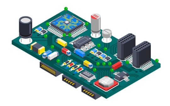
#MOSFET ICs
Explore tagged Tumblr posts
Visit Tumblr Blog
Explore Tumblr blogs with no restrictions, modern design and the best experience.
Last Seen Tumblr Blogs


Fun Fact
Tumblr has 4 main sources of revenue.
Text
Unleashing the Power of Semiconductor ICs
Introduction
Semiconductor Integrated Circuits (ICs) have revolutionized the world of electronics, enabling compact, efficient, and powerful electronic devices. These tiny wonders, made up of various electronic components on a single semiconductor substrate, play a crucial role in modern technology. In this blog post, we will delve into the fascinating realm of Semiconductor ICs, focusing on Audio ICs, Interface ICs, Logic Gate ICs, MOSFET ICs, Optocoupler ICs, Memory ICs, and Sensor ICs. Join us on this captivating journey as we explore the applications, working principles, and advancements in these essential IC categories.
Audio ICs: Enhancing Sound Experience
Audio ICs are designed specifically to process, amplify, and control audio signals. These ICs find applications in a wide range of audio devices, including smartphones, music players, home theater systems, and car audio systems. They play a crucial role in delivering high-quality sound with features like amplification, filtering, and audio signal processing. From delivering immersive music experiences to enabling crystal-clear voice calls, Audio ICs make our audio devices come alive.
Interface ICs: Bridging the Digital Divide
Interface ICs act as intermediaries, facilitating communication and data transfer between different electronic components or systems. They enable seamless connectivity by converting signals between different voltage levels, formats, or protocols. These ICs find applications in devices like USB interfaces, display controllers, and communication modules. With their ability to bridge the digital divide, Interface ICs empower diverse devices to work together harmoniously.
Logic Gate ICs: Building the Foundation of Digital Circuits
Logic Gate ICs are fundamental building blocks of digital circuits. They perform logical operations such as AND, OR, and NOT, enabling the manipulation and processing of binary data. These ICs are the backbone of digital systems, including microprocessors, memory units, and control units. Logic Gate ICs make complex computations and decision-making possible, providing the intelligence behind our digital devices.
MOSFET ICs: Powering Electronic Switching
Metal-Oxide-Semiconductor Field-Effect Transistor (MOSFET) ICs are essential for power management and electronic switching applications. These ICs offer high efficiency, low power consumption, and fast switching capabilities. They find applications in power supplies, motor control, and various electronic circuits that require efficient power handling. MOSFET ICs play a crucial role in optimizing power usage and enabling energy-efficient electronic devices.
Optocoupler ICs: Isolating and Protecting Signals
Optocoupler ICs, also known as optoisolators, are designed to provide electrical isolation between input and output signals. They utilize light-emitting diodes (LEDs) and phototransistors to transmit signals without direct electrical connection. Optocoupler ICs are commonly used in situations where signal isolation, noise reduction, or protection against voltage spikes is required. They find applications in industries such as telecommunications, industrial automation, and medical equipment, ensuring reliable and safe signal transmission.
Memory ICs: Storing and Retrieving Data
Memory ICs are responsible for storing and retrieving digital data in electronic devices. These ICs come in various forms, such as Static Random Access Memory (SRAM) and Flash memory. Memory ICs are vital components of computers, smartphones, gaming consoles, and other data-intensive devices. They enable rapid data access, high-speed data transfer, and non-volatile storage, ensuring seamless user experiences and efficient data management.
Sensor ICs: Sensing the World Around Us
Sensor ICs are designed to detect and measure physical phenomena, converting them into electrical signals for further processing. They enable devices to sense various parameters such as temperature, pressure, motion, light, and proximity. Sensor ICs find applications in diverse fields, including automotive, healthcare, environmental monitoring, and consumer electronics. From enabling accurate navigation in smartphones to facilitating precise environmental monitoring, Sensor ICs make our devices smarter and more responsive.
Conclusion
Semiconductor ICs have reshaped the world of electronics, powering our devices with unprecedented functionality, efficiency, and miniaturization. In this blog post, we explored the remarkable applications and advancements in Audio ICs, Interface ICs, Logic Gate ICs, MOSFET ICs, Optocoupler ICs, Memory ICs, and Sensor ICs. These ICs play pivotal roles in delivering enhanced audio experiences, bridging digital gaps, enabling digital logic, managing power efficiently, providing signal isolation, storing and retrieving data, and sensing the world around us. As we continue to push the boundaries of technology, Semiconductor ICs will undoubtedly remain at the forefront of innovation, driving the next wave of breakthroughs in electronics.
0 notes
Text
https://www.futureelectronics.com/p/semiconductors--discretes--transistors--mosfets/irfr3607trpbf-infineon-6174095
Surface Mount Trench Power MOSFET, MOSFET transistors, ic mosfet
Single N-Channel 75 V 9 mOhm 84 nC HEXFET® Power Mosfet - TO-252-3
#Transistors#Mosfets#IRFR3607TRPBF#Infineon#Surface Mount Trench Power#ic mosfet#FM radio transmitter circuit#mosfet circuits#mosfet switch#mosfet uses#Mosfet gate#Mosfet#mosfet transistor#Types of mosfet
1 note
·
View note
Text
https://www.futureelectronics.com/p/semiconductors--analog--drivers--mosfet-igbt-drivers/bts4175sgaxuma1-infineon-5060642
What is an IGBT driver, mosfet gate driver, high side, ic, MosFet driver chip
BTS4175SGA Series 52 V 1.3 A Smart High Side Power Switch - PG-DSO-8
#Drivers#MOSFET / IGBT Drivers#BTS4175SGAXUMA1#Infineon#mosfet gate driver#high side#ic#MosFet driver chip#circuit#High side MosFet driver#MosFet driver#IGBT gate driver#what is a mosfet driver#P channel MosFet driver#Low side
1 note
·
View note
Text
https://www.futureelectronics.com/p/semiconductors--discretes--transistors--mosfets/irf644pbf-vishay-4156743
High current mosfet, mosfet switch, mosfet module, mosfet applications
Single N-Channel 250 V 0.28 Ohms Flange Mount Power Mosfet - TO-220AB
#Vishay#IRF644PBF#Transistors#Mosfets#High current mosfet#mosfet switch#mosfet module#mosfet applications#How mosfet works#mosfet transistor#Mosfet switch circuit#how mosfet works#circuits#IC Mosfet#mosfet gate
1 note
·
View note
Text
https://www.futureelectronics.com/p/semiconductors--discretes--transistors--mosfets/dmg1012uw-7-diodes-incorporated-6129534
Mosfet applications, Mosfet transistor, mosfet module, mosfet function
N-Channel 20 V 1 A 0.45 Ω Surface Mount Enhancement Mode Power MosFet - SOT-323
#Diodes Incorporated#DMG1012UW-7#Transistors#Mosfets#transistor mosfet#IC mosfet#Mosfet switch circuit#how mosfet work applications#mosfet module#mosfet function High voltage mosfet#Power mosfet#mosfet circuits#mosfet gate#Types of mosfet
1 note
·
View note
Text
#transistors#electronics#transistor#diodes#resistors#led#mosfet#capacitors#microcontroller#sensors#optocoupler#ic#microchip#pcba#electroniccomponents#module#diy#arduino#thyristor#diode#igbt#mosfets#microprocessor#connectors#mcu#dram#chips#crystals#electrical#electricalengineer
1 note
·
View note
Text
Orange Bass Terror 1000
This amp really gave me a hard time. This amp belongs to the bass player for my band. The original issue was that the signal would cut out in the middle of practice or shows and the head would just fizzle out and shut down.

My initial thoughts were that the class D power amp was failing due to overheating. On the bench, heat seemed fine, fan kicked on with no issues and parts weren’t getting too hot, but voltages were not normal in the power supply. These amps have a smps mounted on the top of the amp.


I spent some time replacing dodgy electrolytic caps in the switching part of the power supply. Didn’t help. I flipped the amp over, voltages seemed okay for the most part but at the first power amp mosfet, there was a short between all three legs. I replaced that mosfet and the amp started to blowing fuses every time I powered it up on the variac and the fan and indicator light weren’t turning on anymore. Tracing that back through the power supply, one of the switching mosfets had failed causing the bridge rectifier, and power switching IC to fail as well. I replaced the mosfets, the IC, and the bridge rectifier.
Now we had decent voltages to most of the amp except for the -53V rail which was way off.
I started testing diodes and found that D5 in the power amp was shorted.


Of course that diode is totally inaccessible without removing the huge inductor. Once the inductor was out, the diode wasn’t reading short anymore. I was able to trace this back and the only thing that made sense was another failing power amp mosfet.

I went through and replaced the rest of the power amp mosfets and we were rocking.
Special thanks to my Rigol DS1052E on this one. Couldn’t have done it without you.
-Kaden
2 notes
·
View notes
Text
What is PCB Assembly ?
PCB Assembly manufacturer - Hitech Circuits Co., Limited
It’s the step in the manufacturing process in which you populate a blank board with the electronic components needed to make it into a functional printed circuit board. It’s these components that make a board into the circuit that enables an electronic product to function. PCB assembly typically takes place via one of two processes:
1. Surface-mount technology
SMT: SMT stands for “Surface Mount Technology“. The SMT components are very small sizes and comes in various packages like 0201, 0402, 0603, 1608 packages for resistors and capacitors. Similarly for Integrated circuits ICs we have SOIC, TSSOP, QFP and BGA.
The SMT components assembly is very difficult for human hands and can be time taking process so it is mostly done by automated pick and place machine.
2. Through-hole manufacturing
THT: THT stands for “Through hole Technology”. The components with leads and wires, like resistors, capacitors, inductors, PDIP ICs, transformers, transistors, IGBTs, MOSFETS are example.
The component has to be inserted on one side of PCB and pulled by leg on other side and cut the leg and solder it. The THT components assembly is usually done by hand soldering and is relatively easy.
Printed Circuit Board Assembly Techniques
There are only two common PCBA techniques available for use by a PCB designer. The methods are:
1. Automated PCB Assembly Techniques
Generally, this technique employs the use of state of the art machines, which are fully automatic. For example, the surface mount components are worth positioning with the aid of an automated pick and place machine.
Again, reflow soldering is commonly for surface mount components usually done in a reflow oven. An automated solder stencil is also used to apply the solder paste on the PCB.
Finally, high tech inspection machines are used to confirm and check the quality of the PCBA. Some of which include: Automated optical inspection machine (AOI), X-ray inspection machines, etc.
Above all, due to the precise monitoring, control of soldering, no human input and versatile machines.
This technique ensures utmost efficiency, output consistencies, and limits defects.
2. Manual PCB Assembly Techniques
This method is favorite for use with through-hole parts, which needs manual placement on the board. Besides, with these through-hole parts, it’s advisable you use wave soldering. Note that in the through- hole assembly process, you need to place the components and electronics on the PCB.
After that, you use wave soldering to solder the leads. Typically, you will need an individual to insert a component into a marked PTH. Once done, transfer the PCB to the next station where the next person will be on standby tasked with fixing another part.
What are the Benefits of SMT PCB Assembly?
SMT assembly provides many benefits and some of them are as follows:
It can be used to incorporate small components.
In SMT, the components can be placed on both sides of the board.
It assures high component densities.
Fewer holes need to be drilled for surface mounting than through-hole.
It require low initial costs and time for setting up the mass production.
SMT is the simpler and faster-automated assembly when compared to through-hole.
Errors regarding the component placement can be easily rectified.
Surface mount PCBs feature strong joints, which can easily withstand vibrations.
What are the techniques used in Surface Mount Technology?
There are several techniques for the reflow process. After applying the solder paste or a flux mixture on the board and after placing the components, the boards are conveyed to a reflow soldering oven. The techniques used for reflowing soldering include infrared lamps, hot gas convection, fluorocarbon liquids with a high boiling point, and so on.
What are the different testing methods used in SMT PCB Assembly?
Hitech Circuits as the PCB assembly manufacturer, we perform the following testing and inspection to ensure the quality of surface mount PCBs.
Automated Optical Inspection (AOI): This is performed before and after the soldering to identify the component placement, presence, and solder quality.
X-ray Testing: In this type of testing, the operator relies on the X-ray images of the PCB to check the solder joints and lead-less components such as Quad Flat Packs and ball grid arrays, which are generally not visible to naked eyes.
In-Circuit Testing (ICT): This method is used to detect manufacturing defects by testing the electrical properties in the SMT Assembly.
What type of files or documents should I send for SMT PCB Assembly?
Gerber Files: The file contains all details of physical board layers including solder masks, copper layers, drill data, legends, and so on.
Bill of Materials (BOM): This contains information on the list of items needed for the PCB manufacturing and the instructions of manufacturing.
Pick and Place File: This file contains information on all components to be used in the PCB design and their rotation and X-Y coordinates.
The whole process of PCB Assembly
1. Bare board loader machine
The first step in the PCB assembly is to arrange the bare boards on the rack, and the machine will automatically send the boards one by one into the SMT assembly line.
2. Printing solder paste
When PCB on the SMT production line, firstly, we have to print solder paste on it, and the solder paste will be printed on the pads of the PCB. These solder pastes will be melt and solder the electronic parts to the circuit board when it passes through the high-temperature reflow oven.
In addition, when testing new products, some people will use film board/adhesive cardboard instead of solder paste, which can increase the efficiency for adjusting the SMT machines.
3. Solder paste inspection machine(SPI)
Since the quality of solder paste printing is related to the quality of welding of subsequent parts, some SMT factories will use optical machine to check the quality of solder paste after printed the solder paste in order to ensure stable quality. If there any poorly printed solder paste board, we will wash off the solder paste on it and reprint, or remove the excess solder paste if there is redundant solder paste on it.
4. High speed SMT machine
Usually, we will put some small electronic parts (such as small resistors, capacitors, and inductors) to be printed on the circuit board first, and these parts will be slightly stuck by the solder paste just printed on the circuit board, so even if the speed of printing is very fast and the parts on the board will not fall away. But large parts are not suitable for use in such high speed SMT machines, which will slow down the speed of small parts assembly. And the parts will be shifted from the original position due to the rapid movement of the board.
5. Universal SMT machine
Universal SMT machine is also known as "slow machine", it will be assembled some large electronic components, such as BGA IC, connectors, etc., these parts need more accurate positions, so the alignment is very important. Use a camera to take a picture to confirm the position of the parts, so the speed is much slower than High speed SMT machine we taked before. Due to the size of the components here, not all of them are packed in tape and reel, and some may be packed in trays or tubes. But if you want the SMT machine to recognize the trays or tube-shaped packaging materials, you must configure an additional machine.
Generally, traditional SMT machines are using the principle of suction to move electronic parts, and in order to place the parts successfully, and there must be the flat surface on these electronic components for the suction nozzle of the SMT machine to absorb. However, for some electronic parts don’t have a flat surface for these machines, and it is necessary to order special nozzles for these special-shaped parts, or add a flat tape on the parts, or wear a flat cap for thees electronic parts.
6. Manual parts or visual inspection
After assembled all parts by the high speed SMT machine or Universal SMT machine and before going through the high-temperature reflow oven, and we will set up a visual inspection station here and to pick out the deviation parts or missing components boards etc., because we have to use a soldering iron to repair if there are still defectives boards after passing the high-temperature oven, which will affect the quality of the product and will also increase the cost. in addition, for some larger electronic parts or traditional DIP parts or some special reasons cannot be processed by the SMT machine before, they will be manually placed on pcb here.
7. Reflow oven
The purpose of reflow oven is to melt the solder paste and form a non-metallic compound on the component feet and the circuit board, that means to solder electronic components on the circuit board. The temperature rise and fall curves often affect the soldering quality of the entire circuit board. According to the characteristics of the solder materials, usually the reflow oven will set the preheating zone, soaking zone, reflow zone, and cooling zone to achieve the best soldering effect.
For example, the melting point for SAC305 solder paste with lead-free is about 217°C, which means that the temperature of the reflow oven must be higher than the melting points to remelt the solder paste. What's more, the maximum temperature in the reflow furnace should not exceed 250°C, otherwise many parts will be deformed or melted because they cannot withstand such a high temperature.
Basically, after the pcb passed through the reflow oven, the assembly for the entire circuit board is almost complete. If there are hand-soldered parts, we need to transfer to DIP process, and then we have to check the quality after reflow oven by QC department.
8. Automatic optical inspection(AOI)
The main purpose of setting up AOI is because some high density boards can’t be process the following ICT test, so we used AOI inspection to replace it. But even using AOI inspections, there still have the blind spots for such checking, for example, the solder pads under the components cannot be checked by AOI. At present, it can only check whether the parts have side standing issue, missing parts, displacement, polarity direction, solder bridges, lack of soldering etc., but cannot checking the BGA solderability, resistance value, capacitance value, inductance value and other components quality, so far AOI inspection can’t completely replace ICT test.
Therefore, there is still some risk if only AOI inspection is used to replace ICT testing, but ICT test is also not 100% make sure the good quality, we suggest these two ways can be combined with together to make sure the good quality.
9. PCB unloader machine
After the board is fully assembled, it will be retracted to the unloder machine, which has been designed to allow the SMT machine to automatically pick and place the board without damaging the quality for PCB.
10. Visual inspection for finished products
Normally there will be a visual inspection area in our SMT production line whether there is an AOI station or not, and it will help to check if there are any defectives after completed assembled the pcbs. If there is an AOI station, it can reduce the visual inspection worker on our SMT line, and to reduce the potential cost, and because it is still necessary to check some places that cannot be judged by AOI, many SMT factories will provide the mainly visual inspection templates at this station, which is convenient for visual inspection worker to inspect some key parts and polarity for components.
11. DIP process
DIP process is a very important process in the whole PCBA processing, and the processing quality will directly affect the functional for PCBA boards, so it is necessary to pay more attention to the DIP process. There are many preliminary preparations for DIP process. The basic process is to re-process the electronic components first, like to cut the extra pins for some DIP components, our staff received the components according to the BOM list, and will check whether the material part numbers and specifications are correct or not, and performs pre-production pre-processing according to the PCBA samples. The steps are: Use various related equipment (automatic capacitor pins cutting machine, jumper bending machine, diode and triode automatic forming machine, automatic belt forming machine and other machines) for processing.

12. ICT test
Printed Circuit board open/short circuit test (ICT, In-Circuit Test), The purpose of ICT test is mainly to test whether the components and circuits on the printed circuit board are open or short issues. It can also measure the basic characteristics of most components, such as resistance, capacitance, and inductance values to judge whether the functions of these parts are damaged, wrong parts or missing parts etc. after passing through the high-temperature reflow oven.
ICT test machines are divided into advanced and basic machines. The basic ICT test machines are generally called MDA (Manufacturing Defect Analyzer). It’s just to measure the basic characteristics of electronic components and judge open and short circuits issue we talked above.
In addition to all the functions of the basic ICT test machines, for advanced ICT test machine can also test the whole PCBA by using power, start to testing the PCBA boards by setting the program in the test machine. The advantage is that it can simulate the function of the printed circuit board under the actual power-on condition, this test can partly replace the following functional test machine (Function Test). But the cost for the test fixture of this advanced ICT test can probably buy a car, it’s too expensive and we suggest it can be used in mass production products.
13. PCBA function test
Functional testing is to make up for the ICT test, because ICT only tests the open and short circuits on the the PCBA board, and other functions such as BGA and other fuctions are not tested, so it is necessary to use a functional testing machine to test all functions on the whole PCBA board.
14. Cutting board (assembly board de-panel)
Normally, printed circuit boards will be produced in panel, and it will be assembled to increase the efficiency of SMT production. It means several single boards in one panel, such as two-in-one, four-in-one etc. After finished all the pcb assembly process, it needs to be cut into single boards, and for some printed circuit boards with only single boards also need to cut off some redundant board edges.
There are several ways to cut the printed circuit board. You can design the V-cut using the blade cutting machine (Scoring) or directly manually break off the board (not recommended). For more high density circuit boards, it will be used the professional splitting machine or the router to split the board without any damage the electronic components and printed circuit boards, but the cost and working hours will be a little longer.
Why Choose Hitech Circuits PCB Assembly Manufacturer for Your PCB Assembly Projects?
There are several PCB manufacturers specializing in PCB assemblyservices. However, Hitech Circuits PCB Assembly stands out owing to the following:
Assistance in Material Procurement:
Technically, in PCB assembly services, the quality of parts is the responsibility of the OEM; however, we ease your job by assisting you to make the right selection. We can help you procure all your parts of the same type own a single part number, thanks to our supply chain and vendor network as well as experience. This saves time and cost that goes in ordering single parts as you plan.
Testing procedures:
We are very focused on quality and thus implement stringent testing procedures at each stage of the assembly and after completion.
Fast Turnaround Times:
Our well-equipped facility and the right tools enable us to complete your requirements well before time, and without compromising on the quality or functioning of the PCBs. For simple designs we revert in 24 to 48 hours.
Cost Effectiveness:
While PCB assembly is a cost-effective alternative, we go a step further and assure that the parts you list are of a good quality and suitable for your requirement. Also, you can control the part flow and replenish them as needed. This eliminates the need to buy extra stock and store it.
Quick Quote:
We offer a quick quote based on your BOM. All you need is a detailed BOM, Gerber files, your application requirement sheet, and quantity.
We’re not one to stand still, which is why we use the latest equipment and the finest minds to create your PCB projects. We’re constantly keeping our finger on the pulse of the latest trends. And as a result, we know how to deliver the highest standards of PCB assembly to meet all your requirements.
Our dedicated, friendly customer service team also means that we support you every step of the way. Offering our expert guidance to ensure a complete PCB project that you’re happy with.
Contact us today
No matter what your printed circuit board assemblyneeds are, we always aim to deliver efficient, dependable solutions. For more information about our services, do not hesitate to get in touch with us today for a no-obligation quote
2 notes
·
View notes
Text
Strobe Overdrive Digital Controller Market: Key Developments and Investment Opportunities 2025–2032

MARKET INSIGHTS
The global Strobe Overdrive Digital Controller Market size was valued at US$ 156.8 million in 2024 and is projected to reach US$ 223.4 million by 2032, at a CAGR of 4.5% during the forecast period 2025-2032.
Strobe Overdrive Digital Controllers are specialized electronic devices that regulate stroboscopic lighting in LED applications through precise voltage pulse modulation. These controllers enhance LED lifespan by minimizing heat generation through controlled short-duration illumination cycles. The technology finds extensive application in machine vision systems, industrial inspection, and high-speed imaging where precise lighting control is critical.
The market growth is driven by increasing automation in manufacturing sectors and rising demand for machine vision systems, which grew 12% year-over-year in 2023. While North America currently dominates with 38% market share, Asia-Pacific is emerging as the fastest-growing region due to rapid industrialization. Key players including Basler AG and CCS Inc. are expanding their product portfolios to include multi-channel controllers, which accounted for 62% of 2024 sales.
MARKET DYNAMICS
MARKET DRIVERS
Growing Adoption of Machine Vision Systems to Fuel Demand for Strobe Overdrive Digital Controllers
The global surge in industrial automation is accelerating demand for machine vision systems, which rely heavily on precision lighting solutions like strobe overdrive digital controllers. These controllers enable high-speed imaging by synchronizing ultra-short LED flashes with camera exposures, eliminating motion blur in fast-moving production lines. The machine vision market is projected to grow at over 7% annually, driven by quality inspection needs in automotive, electronics, and pharmaceutical sectors. Strobe controllers have become indispensable in applications requiring microsecond-level timing accuracy, such as semiconductor wafer inspection where defects as small as 10 microns must be detected.
Energy Efficiency Regulations Driving LED Lighting Upgrades
Stringent global energy efficiency standards are prompting widespread replacement of conventional lighting with advanced LED systems. Strobe overdrive controllers extend LED lifespan by 300-400% through precise thermal management, making them essential components in commercial and industrial lighting upgrades. The lighting control market is experiencing 15% year-over-year growth in smart buildings segment, where strobe-enabled emergency lighting systems now represent over 35% of new installations. Production facilities implementing Industry 4.0 standards particularly benefit from the combination of high-efficiency lighting and machine vision capabilities enabled by advanced digital controllers.
Technological Advancements in High-Speed Imaging
Recent breakthroughs in CMOS sensor technology allow industrial cameras to capture images at over 1,000 frames per second, creating parallel demand for ultra-fast lighting synchronization. Modern strobe overdrive controllers now achieve pulse widths below 1 microsecond with rise times under 100 nanoseconds, enabling crisp imaging of rapidly moving machinery components. The automotive manufacturing sector alone accounts for 28% of high-speed imaging applications, where strobe controllers help detect assembly line defects in real-time. Continued R&D investments by major players have yielded controllers with 32-bit resolution timing and Ethernet-based synchronization capabilities that support Industry 4.0 networking standards.
MARKET RESTRAINTS
Supply Chain Disruptions Affecting Electronic Components Availability
The strobe overdrive controller market faces significant challenges from ongoing semiconductor shortages and supply chain volatility. Critical components like high-power MOSFETs and precision timing ICs have seen lead times extend to 52 weeks in some cases, disrupting production schedules across the industry. A recent survey indicated that 68% of industrial automation suppliers experienced delays in controller shipments due to component shortages. This has created a ripple effect, with machine vision system integrators reporting project postponements worth an estimated $450 million in deferred revenue during the past fiscal year.
Complex Integration Requirements in Legacy Systems
While modern industrial facilities readily adopt advanced controllers, retrofitting legacy manufacturing equipment presents significant technical hurdles. Many older systems lack standardized communication interfaces, requiring custom integration solutions that can increase project costs by 40-60%. The automotive sector reports that nearly 35% of its existing production lines require substantial modifications to implement modern strobe lighting systems. Additionally, synchronization between multiple controllers in large-scale applications remains challenging, with timing jitter below 10 nanoseconds proving difficult to maintain across distributed systems.
High Initial Costs for Advanced Systems
Premium multi-channel strobe controllers with network synchronization capabilities command price points 2-3 times higher than basic models, creating adoption barriers for small and medium enterprises. Industrial users report that complete vision system overhauls including advanced controllers require capital expenditures averaging $250,000 per production line. While the ROI justification exists for high-volume manufacturers, the upfront costs deter many potential customers in lower-margin industries. This pricing sensitivity has slowed market penetration in developing regions where industrial automation adoption is still in early stages.
MARKET CHALLENGES
Thermal Management in High-Density Applications
As industrial applications demand higher flash intensities and faster repetition rates, thermal dissipation becomes a critical challenge. Modern controllers must manage instantaneous power levels exceeding 5 kW while maintaining case temperatures below automotive-grade specifications of 85°C. Field failures due to thermal stress account for approximately 18% of warranty claims in the industry. The transition to gallium nitride (GaN) power semiconductors promises improvements but introduces new challenges in circuit design and manufacturing consistency.
Precision Timing in Distributed Systems
Synchronization accuracy deteriorates as strobe systems scale across large facilities spanning hundreds of meters. Maintaining sub-microsecond timing precision requires complex network architectures with specialized timing protocols. The aerospace manufacturing sector reports unacceptable variation (>50 ns) in 12% of multi-controller installations, forcing expensive workarounds. Emerging IEEE 1588 Precision Time Protocol implementations show promise but require extensive validation in industrial environments with electromagnetic interference.
Standardization Across Ecosystem
The lack of uniform communication protocols between controllers, cameras, and automation systems creates integration bottlenecks. While GenICam provides a framework for vision components, proprietary extensions from major vendors fragment the market. System integrators report spending 30-45% of project time on custom interface development rather than application optimization. The industry's transition to OPC UA over TSN promises long-term solutions but will require substantial retooling of existing installations.
MARKET OPPORTUNITIES
Emerging Applications in Autonomous Robotics
The rapid growth of mobile robotics in warehouses and fulfillment centers presents significant opportunities for advanced strobe controllers. Autonomous guided vehicles (AGVs) require robust vision systems capable of operating under variable ambient light conditions. Early adopters report 40% improvement in barcode reading reliability when implementing strobe synchronization at throughput rates exceeding 2,000 packages per hour. The global AGV market is projected to maintain 12% CAGR through 2030, creating parallel demand for ruggedized controllers that withstand vibration and environmental stressors.
Expansion into Biomedical Imaging
High-speed microscopy and surgical imaging systems increasingly incorporate strobe lighting for reduced phototoxicity and improved image contrast. The life sciences sector represents one of the fastest growing verticals for precision controllers, with adoption increasing at 22% annually. Recent developments in multi-spectral strobe systems enable advanced fluorescence imaging techniques while meeting stringent medical safety standards. Controller manufacturers specializing in biomedical applications command premium pricing with gross margins exceeding 60%.
Integration with AI-Based Visual Inspection
The convergence of machine vision with artificial intelligence creates new requirements for adaptive lighting control. Modern defect detection algorithms achieve highest accuracy when provided with optimally illuminated multi-angle views. Smart controllers that dynamically adjust strobe parameters based on AI feedback demonstrate 35% improvement in detection rates compared to static configurations. Leading automotive manufacturers report first-pass yield improvements of 2-3% when implementing AI-driven strobe systems, translating to annual savings exceeding $15 million per production facility.
STROBE OVERDRIVE DIGITAL CONTROLLER MARKET TRENDS
Growth in Machine Vision Applications Driving Market Expansion
The global strobe overdrive digital controller market is experiencing significant growth due to increasing adoption in industrial machine vision systems. These controllers enable precise synchronization between cameras and LED lighting, improving inspection accuracy in manufacturing lines. The food packaging sector alone accounts for approximately 28% of industrial machine vision applications, creating substantial demand for advanced lighting controllers. Furthermore, automotive quality control systems are integrating strobe controllers at a compound annual growth rate of 12.4%, driven by the need for high-speed defect detection in production environments.
Other Trends
Energy Efficiency Regulations
Stringent energy efficiency mandates worldwide are accelerating the shift toward digital lighting control solutions. Strobe overdrive controllers reduce LED power consumption by up to 40% compared to continuous lighting modes, while maintaining equivalent illumination output. This energy-saving capability has become particularly valuable in Europe, where industrial facilities face mounting pressure to meet EU Ecodesign Directive 2021 requirements. The technology's ability to extend LED lifespan through thermal management further enhances its sustainability credentials.
Industrial Automation Integration
The proliferation of Industry 4.0 initiatives is creating robust demand for smart lighting control solutions that can interface with automated production systems. Leading manufacturers are developing controllers with EtherCAT and PROFINET compatibility, enabling seamless integration into digital factory networks. In 2024, nearly 62% of new industrial strobe controllers shipped included industrial Ethernet connectivity, reflecting this trend. Smart Vision Lights and other innovators are now offering controllers with built-in machine learning algorithms that automatically adjust lighting parameters based on object detection feedback.
Technological Advancements in Controller Design
Recent product developments focus on improving pulse timing precision below 1 microsecond accuracy, critical for high-speed manufacturing applications. Multi-channel configurations now represent 38% of the market, allowing synchronized control of multiple light sources from a single unit. The introduction of touchscreen interfaces and wireless configuration options has significantly improved usability, reducing setup times by approximately 25% compared to traditional rotary dial controllers. Meanwhile, IP65-rated enclosures are becoming standard for harsh industrial environments, with demand growing at 15% annually in the chemicals and pharmaceuticals sectors.
COMPETITIVE LANDSCAPE
Key Industry Players
Innovation and Strategic Expansion Define Market Leadership
The global Strobe Overdrive Digital Controller market features a mix of established leaders and emerging innovators, all competing to secure a stronger foothold in this specialized segment. The landscape is semi-consolidated, with key players leveraging technological expertise and strategic partnerships to differentiate themselves. Leading the market is CCS Inc, which holds a significant share due to its advanced strobe control solutions and robust presence across industrial and commercial applications. The company’s success stems from its high-precision controllers that optimize LED performance in machine vision and automation.
Basler AG and SVS-Vistek follow closely, capitalizing on their strong R&D capabilities and diversified product portfolios. These companies have been pivotal in driving adoption across North America and Europe, where demand for energy-efficient lighting control solutions continues to grow. Their focus on integrating smart diagnostics and IoT compatibility into strobe controllers has further strengthened their market position.
Meanwhile, MORITEX Corporation and Smart Vision Lights are expanding aggressively in Asia-Pacific, particularly in Japan and China, where industrial automation investments are surging. These players are actively launching multi-channel strobe controllers with enhanced synchronization features, catering to high-speed imaging applications in manufacturing and logistics. Their ability to offer customized solutions gives them a competitive edge in niche markets.
Smaller but rapidly growing companies like Gardasoft and VS Technology are making strides through innovation, particularly in enhancing pulse-width modulation (PWM) efficiency. These firms are gaining traction among SMEs by offering cost-effective alternatives without compromising on performance. Their agility in adapting to customer-specific requirements positions them well for long-term growth.
The market is witnessing a surge in partnerships as companies collaborate to integrate strobe controllers with broader automation ecosystems. For instance, recent alliances between strobe controller manufacturers and machine vision software providers aim to streamline operations in smart factories, further expanding revenue opportunities.
List of Key Strobe Overdrive Digital Controller Companies Profiled
CCS Inc (Japan)
SVS-Vistek (Germany)
Basler AG (Germany)
MORITEX Corporation (Japan)
Smart Vision Lights (U.S.)
Gardasoft (U.K.)
Opto Engineering (Italy)
Stemmer Imaging (Germany)
OPT Machine Vision Tech (China)
VS Technology (Japan)
Segment Analysis:
By Type
Single Channel Segment Dominates Owing to Cost-Effective Deployment in Small-Scale Applications
The market is segmented based on type into:
Single Channel
Multi-channel
By Application
Business Premises Application Leads Due to Rising Demand for Industrial Machine Vision Systems
The market is segmented based on application into:
Residential
Business Premises
Others
By Technology
LED-Based Controllers Gain Traction Due to Energy Efficiency and Extended Lifespan
The market is segmented based on technology into:
LED-based
Xenon-based
Others
By End-Use Industry
Manufacturing Sector Accounts for Major Share with Increasing Automation Adoption
The market is segmented based on end-use industry into:
Manufacturing
Automotive
Electronics
Healthcare
Others
Regional Analysis: Strobe Overdrive Digital Controller Market
North America North America remains a critical market for strobe overdrive digital controllers, driven by the strong presence of automation-focused industries and technological advancements. Major manufacturers like Smart Vision Lights and OPT Machine Vision Tech operate extensively in this region, particularly benefiting from the U.S. market, which accounts for a significant revenue share. The demand is bolstered by applications in machine vision, industrial inspection, and LED-based lighting solutions. Additionally, regulatory pressures for energy-efficient lighting systems further accelerate adoption. While Canada and Mexico show steady growth, investment in automation and IoT-driven processes positions North America as a leader in high-performance strobe controller adoption.
Europe Europe's strobe overdrive digital controller market thrives on stringent industrial automation standards and a mature manufacturing sector. Countries like Germany, France, and the U.K. lead the adoption of advanced strobe lighting solutions, primarily driven by automotive, pharmaceuticals, and electronics sectors. Compliance with EU directives on energy efficiency and precision lighting has pushed companies such as Basler AG and Stemmer Imaging to innovate in multi-channel controllers. However, high operational costs and saturation in certain industrial segments moderate growth. Nonetheless, increasing automation in Eastern Europe presents untapped potential for the market.
Asia-Pacific The Asia-Pacific region dominates the strobe overdrive digital controller market in terms of volume, propelled by rapid industrialization in China, Japan, and India. Leading suppliers like MORITEX Corporation and Opto Engineering capitalize on expanding manufacturing bases and infrastructure investments. China’s electronics and semiconductor industries fuel substantial demand for precision lighting controls, while India’s growing automation sector presents emerging opportunities. Despite cost sensitivity favoring single-channel controllers, the shift toward smart factories and inspection technologies drives gradual adoption of advanced solutions across the region.
South America South America’s strobe overdrive digital controller market is evolving, with Brazil and Argentina witnessing growing applications in food processing and automotive manufacturing. However, economic instability and fragmented industrial policies hinder widespread adoption. Local players struggle with import dependencies, while multinational suppliers target niche high-value applications. The market shows potential in Brazil due to incremental automation investments, but overall progress remains sluggish compared to global counterparts.
Middle East & Africa The Middle East & Africa exhibit nascent but promising growth opportunities, particularly in GCC countries like the UAE and Saudi Arabia, where industrialization and smart city initiatives gain traction. Turkey and Israel also demonstrate increasing adoption in manufacturing and security applications. However, limited local production capabilities and reliance on imports delay market penetration. Africa’s potential remains largely untapped due to infrastructure gaps, though rising foreign investments in automation signal gradual market expansion.
Report Scope
This market research report provides a comprehensive analysis of the global and regional Strobe Overdrive Digital Controller markets, covering the forecast period 2025–2032. It offers detailed insights into market dynamics, technological advancements, competitive landscape, and key trends shaping the industry.
Key focus areas of the report include:
Market Size & Forecast: Historical data and future projections for revenue, unit shipments, and market value across major regions and segments. The Global Strobe Overdrive Digital Controller market was valued at USD million in 2024 and is projected to reach USD million by 2032.
Segmentation Analysis: Detailed breakdown by product type (Single Channel, Multi-channel), application (Residential, Business Premises, Others), and end-user industry to identify high-growth segments and investment opportunities.
Regional Outlook: Insights into market performance across North America, Europe, Asia-Pacific, Latin America, and the Middle East & Africa. The U.S. market size is estimated at USD million in 2024, while China is projected to reach USD million by 2032.
Competitive Landscape: Profiles of leading market participants including CCS Inc, SVS-Vistek, Basler AG, MORITEX Corporation, and Smart Vision Lights, covering their product offerings, R&D focus, and recent developments.
Technology Trends & Innovation: Assessment of emerging technologies in LED stroboscopic lighting control and pulse width modulation techniques.
Market Drivers & Restraints: Evaluation of factors driving market growth such as increasing demand for energy-efficient lighting solutions, along with challenges like supply chain constraints and regulatory issues.
Stakeholder Analysis: Insights for component suppliers, OEMs, system integrators, and investors regarding strategic opportunities in the evolving market ecosystem.
Primary and secondary research methods are employed, including interviews with industry experts, data from verified sources, and real-time market intelligence to ensure the accuracy and reliability of the insights presented.
FREQUENTLY ASKED QUESTIONS:
What is the current market size of Global Strobe Overdrive Digital Controller Market?
->Strobe Overdrive Digital Controller Market size was valued at US$ 156.8 million in 2024 and is projected to reach US$ 223.4 million by 2032, at a CAGR of 4.5% during the forecast period 2025-2032.
Which key companies operate in Global Strobe Overdrive Digital Controller Market?
-> Key players include CCS Inc, SVS-Vistek, Basler AG, MORITEX Corporation, Smart Vision Lights, Gardasoft, Opto Engineering, and Stemmer Imaging, among others.
What are the key growth drivers?
-> Key growth drivers include increasing demand for energy-efficient lighting solutions, growth in industrial automation, and need for extended LED lifespan in commercial applications.
Which region dominates the market?
-> Asia-Pacific is expected to be the fastest-growing region, while North America currently holds a significant market share.
What are the emerging trends?
-> Emerging trends include integration of IoT capabilities, development of smart lighting systems, and adoption of advanced pulse width modulation techniques.
Related Reports:https://semiconductorblogs21.blogspot.com/2025/06/binary-gas-analyzer-market-size-share.htmlhttps://semiconductorblogs21.blogspot.com/2025/06/inverted-light-microscopy-market.htmlhttps://semiconductorblogs21.blogspot.com/2025/06/insulating-functional-devices-market.htmlhttps://semiconductorblogs21.blogspot.com/2025/06/multi-core-computer-processors-market.htmlhttps://semiconductorblogs21.blogspot.com/2025/06/power-factor-correction-choke-market.htmlhttps://semiconductorblogs21.blogspot.com/2025/06/tunable-ultrafast-source-market-key.htmlhttps://semiconductorblogs21.blogspot.com/2025/06/solid-state-remote-power-controller.htmlhttps://semiconductorblogs21.blogspot.com/2025/06/panel-interface-connector-market.htmlhttps://semiconductorblogs21.blogspot.com/2025/06/semiconductor-process-components-market.htmlhttps://semiconductorblogs21.blogspot.com/2025/06/automotive-high-mount-stop-light-market.htmlhttps://semiconductorblogs21.blogspot.com/2025/06/indium-antimonide-detector-alarm-market.htmlhttps://semiconductorblogs21.blogspot.com/2025/06/din-rail-mounted-thermocouple-terminal.htmlhttps://semiconductorblogs21.blogspot.com/2025/06/hbm2-dram-market-competitive-landscape.htmlhttps://semiconductorblogs21.blogspot.com/2025/06/aptamer-based-quartz-crystal.htmlhttps://semiconductorblogs21.blogspot.com/2025/06/helium-neon-laser-tubes-market-analysis.htmlhttps://semiconductorblogs21.blogspot.com/2025/06/semiconductor-structural-components.htmlhttps://semiconductorblogs21.blogspot.com/2025/06/optical-power-and-energy-market-size.html
0 notes
Text
Silent Powerhouses: How igbt rectifiers Are Redefining Industrial Energy Conversion
Picture a bustling manufacturing floor at dawn. Conveyor belts glide, robotic arms pivot with precision, and high-power motors hum in perfect synchrony. All of this choreographed action relies on stable direct current—even though the utility grid delivers alternating current. Converting AC to DC might sound mundane, yet it’s the unglamorous heartbeat of virtually every modern factory, data center, and electric-rail system. Tucked inside control cabinets and power bays, igbt rectifiers are the silent powerhouses making this conversion cleaner, smarter, and dramatically more efficient.
From Diodes to Digital Brains
For decades, silicon diodes and thyristors dominated rectification. They were sturdy, inexpensive, and—let’s be honest—fairly dumb. They could only switch on and off in crude, bulk fashion, producing DC that was rife with voltage ripple and harmonic distortion. That was acceptable in an analog world, but today’s precision-driven operations need better. Enter the Insulated Gate Bipolar Transistor (IGBT): a semiconductor that marries the high-current capability of a bipolar transistor with the fast switching of a MOSFET.
When engineers embed IGBTs in rectifier topologies, the result is a new class of high-frequency converters capable of pulse-width modulation (PWM), soft-start functions, and active power-factor correction. Suddenly, rectification isn’t just about flipping waveform polarity—it’s about sculpting perfect current for sensitive loads, saving megawatts in the process.
A Day in the Life: Humanizing High Tech
Let’s walk in the shoes of Ananya, maintenance lead at a sprawling metro-rail depot in Bengaluru. She remembers the era when traction substations ran on mercury-arc or SCR rectifiers. “It was like taming a dragon,” she jokes. Voltage spikes chewed through bearings, transformers overheated, and harmonics crept back onto the grid. Then came the retrofit: a modular cabinet stuffed with igbt rectifiers. Overnight, the depot saw a 6 % drop in energy losses and, more surprisingly, quieter lines. “Passengers didn’t notice the upgrade,” Ananya says, “but my team sleeps better knowing the system’s self-diagnostics flag issues before they escalate.”
That’s the hidden human upside—less emergency call-outs, more predictive maintenance, and a work culture that shifts from crisis mode to optimization mode.
Under the Hood: Why IGBT Architecture Shines
High-Frequency Switching IGBTs can switch tens of kilohertz, shrinking bulky transformers and filters. Smaller magnetics mean lighter enclosures and better thermal management.
Low Conduction Losses Compared to MOSFETs at high voltage, IGBTs maintain lower on-state resistance, translating into cooler operation and longer component life.
Built-In Protection Advanced gate-driver ICs monitor temperature, current, and voltage in real time, shutting down the device within microseconds if thresholds are breached.
Bidirectional Capability Paired with appropriate circuitry, they enable regenerative braking in electric locomotives, feeding energy back to the grid instead of dumping it as heat.
Sustainability by Design
Energy efficiency isn’t just a line on a spec sheet—it’s a planetary necessity. Traditional 12-pulse SCR rectifiers often hover near 90 % efficiency under ideal loads. Modern PWM-controlled igbt rectifiers push beyond 97 %, slicing gigawatt-hours off cumulative utility bills over their service life. Multiply that by thousands of installations and you have a tangible dent in global CO₂ emissions.
Moreover, precise DC output means motors run cooler, electrolytic capacitors last longer, and upstream generators experience smoother load profiles. Less wear equals fewer raw materials mined, shipped, and processed for replacements—a virtuous cycle of resource conservation.
Beyond the Factory: Emerging Frontiers
Data Centers – Hyperscale operators love IGBT rectifiers for redundant, hot-swappable power shelves that squeeze more watts per rack while meeting stringent harmonic limits (IEEE 519).
Electrolysis for Green Hydrogen – Stable, low-ripple DC is crucial for membrane longevity. As electrolyzer farms scale into the gigawatt realm, PWM rectifiers slash idle losses and enable dynamic ramp-up tied to renewable generation.
EV Hyper-Chargers – Ultra-fast DC stations (350 kW and higher) rely on modular IGBT blocks to convert grid AC into tightly regulated DC that won’t fry delicate vehicle battery chemistries.
Challenges on the Road Ahead
No technology is perfect. IGBT modules are sensitive to over-voltage transients and require sophisticated snubber networks. Their thermal cycling limits call for meticulous heatsink design and, in harsh climates, liquid cooling. Meanwhile, wide-bandgap semiconductors—silicon carbide (SiC) and gallium nitride (GaN)—are nipping at IGBT heels, promising even faster switching and lower losses.
Yet cost remains king. For high-power (≥ 1 MW) applications, mature supply chains and proven robustness keep igbt rectifiers solidly in the lead. Hybrid topologies that mix SiC diodes with IGBT switches already deliver incremental gains without breaking budgets.
Skills and Workforce Implications
Technicians who once wielded soldering irons on analog boards now brandish oscilloscopes with gigahertz bandwidth to capture nanosecond edge transitions. Training programs are evolving: power-electronics courses in Indian ITIs and polytechnics now include gate-drive design, thermal simulation, and module-level repair practices.
For young engineers, this field offers a blend of hands-on tinkering and digital analytics. Predictive-maintenance dashboards stream real-time data—junction temperatures, switching losses, harmonic spectra—turning power rooms into high-tech command centers.
Final Reflections: Small Silicon, Massive Impact
It’s easy to overlook the humble converter tucked behind a metal door. But in the grand choreography of electrification, igbt rectifiers are the quiet conductors, synchronizing renewable surges, feeding smart grids, and keeping industry humming. They exemplify how incremental innovations—faster switches, smarter firmware, better cooling—compound into game-changing efficiency.
Next time you glide on an electric train, boot up a cloud server, or see a wind farm blinking on the horizon, remember: somewhere underneath, tiny gates are opening and closing thousands of times a second, silently shaping the clean-energy era. And that is technology worth celebrating, even if it never seeks the spotlight.
0 notes
Text
Global Synchronous Buck Converter Market: Market Outlook & Forecast to 2032
Global Synchronous Buck Converter Market was valued at USD 5.23 billion in 2024 and is projected to reach USD 8.45 billion by 2032, growing at a CAGR of 6.20% during the forecast period (2025-2032).
Synchronous Buck Converter Market Overview
The Synchronous Buck Converter is a type of DC-DC converter used to step down voltage efficiently while minimizing power losses. Unlike traditional buck converters, synchronous versions utilize a MOSFET instead of a diode, allowing for higher efficiency, especially at low output voltages and high currents.
These converters are widely used in automotive electronics, industrial equipment, computing devices, and medical instruments, thanks to their compact size, fast transient response, and enhanced thermal performance. The synchronous buck converter market comprises hardware components and integrated circuits manufactured by companies like Texas Instruments, Analog Devices, and STMicroelectronics.
This report provides a deep insight into the global Synchronous Buck Converter Market, covering all its essential aspects. This ranges from a macro-overview of the market to micro details of the market size, competitive landscape, development trend, niche market, key market drivers and challenges, SWOT analysis, value chain analysis, etc.
The analysis helps the reader to shape the competition within the industries and strategies for the competitive environment to enhance the potential profit. Furthermore, it provides a simple framework for evaluating and assessing the position of the business organization. The report structure also focuses on the competitive landscape of the Global Synchronous Buck Converter Market. This report introduces in detail the market share, market performance, product situation, operation situation, etc., of the main players, which helps the readers in the industry to identify the main competitors and deeply understand the competition pattern of the market.
In a word, this report is a must-read for industry players, investors, researchers, consultants, business strategists, and all those who have any kind of stake or are planning to foray into the Synchronous Buck Converter Market in any manner.
Get Full Report : https://semiconductorinsight.com/report/global-synchronous-buck-converter-market/
Synchronous Buck Converter Key Market Trends :
Miniaturization of Power Electronics: Rising demand for compact devices is accelerating the use of synchronous buck converters in miniaturized electronic applications.
Efficiency-Centric Designs: Greater focus on energy-efficient power management solutions in IoT and portable devices.
Integration with Digital Power Management ICs: The market is shifting toward highly integrated, programmable converters.
Rise in Industrial Automation: Automated systems and robots are boosting demand for precise and efficient power solutions.
Focus on Renewable and Portable Applications: Growing adoption in solar-powered and off-grid systems.
Synchronous Buck Converter Market Regional Analysis :
North America:Strong demand driven by EVs, 5G infrastructure, and renewable energy, with the U.S. leading the market.
Europe:Growth fueled by automotive electrification, renewable energy, and strong regulatory support, with Germany as a key player.
Asia-Pacific:Dominates the market due to large-scale manufacturing in China and Japan, with growing demand from EVs, 5G, and semiconductors.
South America:Emerging market, driven by renewable energy and EV adoption, with Brazil leading growth.
Middle East & Africa:Gradual growth, mainly due to investments in renewable energy and EV infrastructure, with Saudi Arabia and UAE as key contributors.
Synchronous Buck Converter Market Segmentation :
The research report includes specific segments by region (country), manufacturers, Type, and Application. Market segmentation creates subsets of a market based on product type, end-user or application, Geographic, and other factors. By understanding the market segments, the decision-maker can leverage this targeting in the product, sales, and marketing strategies. Market segments can power your product development cycles by informing how you create product offerings for different segments.
Market Segmentation (by Application)
Industrial Use
Medical
Home Use
Others
Market Segmentation (by Type)
AC Synchronous Buck Converter
DC Synchronous Buck Converter
Key Company
Texas Instruments
Analog Devices
Infineon Technologies
STMicroelectronics
Eaton
ROHM Semiconductor
RICOH Electronics
Cypress Semiconductor
Maxim Integrated
Microchip
ON Semiconductor
Vicor
Semtech
Torex Semiconductor
Intersil
Diodes
Toshiba
Vishay Semiconductor
Get a Detailed Sample Report : https://semiconductorinsight.com/download-sample-report/?product_id=96432
Key Drivers
Surge in Consumer Electronics Production The increase in smart gadgets, wearables, and portable devices is driving the demand for efficient power conversion components.
Advancements in Semiconductor Technology Smaller, faster, and more reliable MOSFETs are enabling the development of high-performance synchronous buck converters.
Industrial Digitization and Automation Digital transformation across industries requires robust and efficient voltage regulators for system stability.
Key Restraints
Complex Circuit Design Synchronous buck converters involve more complex circuitry, raising the cost and difficulty in implementation.
Thermal Management Challenges High power densities can result in thermal management issues, especially in compact devices.
Market Competition and Price Pressure Intense competition among manufacturers often leads to price wars, affecting profit margins.
Key Opportunities
Emergence of Electric Vehicles (EVs) The growing EV market offers vast potential for power-efficient components like synchronous buck converters.
Growth in Medical Electronics Wearable health monitors and portable diagnostics equipment need reliable power management solutions.
Government Push for Energy Efficiency Increased regulatory support for efficient electronics promotes adoption across regions.
Key Challenges
Design Compatibility with Multiple Standards Ensuring compatibility across varied regional and device-specific standards can be difficult.
Supply Chain Disruptions Geopolitical instability and chip shortages affect timely delivery and pricing.
High R&D Costs Continual innovation in power management requires substantial R&D investment.
Customization of the Report
In case of any queries or customization requirements, please connect with our sales team, who will ensure that your requirements are met.
Related Reports :
Contact us:
+91 8087992013
0 notes
Text
What ESD device should I use for 3.7V Li-Ion surge protection?
In the rapidly developing TWS and smart wearable market, limited by the size of the product and the threat of static electricity and surges in the instant of the battery contact switch, a precise protection of the ESD device is needed to ensure the safety of the power supply IC, from static electricity, surge threats.

The product supports surge 45A, and maintains a margin, support surge voltage greater than 100V, in harsh environments can also be guaranteed to work normally.
Compared with ESD5651N-2/TR, Leiditech Electronics has a greater ipp capability of 1 0A current and a better delivery time, please request samples.
Leiditech Electronics is committed to becoming a leading brand in electromagnetic compatibility (EMC) solutions and component supply. We offer a wide range of products, including ESD, TVS, TSS, GDT, MOV, MOSFET, Zener diodes, and inductors. With an experienced R&D team, we provide personalized customization services to deliver the highest quality EMC solutions tailored to our customers’ needs.
If you’d like to learn more or have any questions, don’t hesitate to reach out:
Visit us at [en.leiditech.com]
#EMCProtection #ESDSafety #WearableTech #Leiditech #SmartDevices #SurgeProtection #ElectronicsDesign #BatterySafety #TWSInnovation #PowerProtection #IoTSecurity #TechSolutions #LiIonBattery #ElectronicsEngineering
0 notes
Text
A Better Way to Source Electronic Components in India
If you've ever tried to order electronic components in India, you’ll know the process isn’t always smooth. Sometimes the delivery is late. Sometimes the parts are wrong—or worse, they aren’t genuine. And if something goes wrong, good luck getting any real support.
That’s where OM Electronic makes a difference. They aren’t just another seller; they understand what sourcing components really involves—especially when precision, time, and reliability matter.
Why It’s Not Enough to Just Buy Electronic Components Online
Yes, you can buy electronic components online from many places. But here’s the reality: not all suppliers are dependable. Some list out-of-stock parts. Some ship counterfeits. Some just vanish after you place the order.
The risk is real. And when your project timeline depends on a single IC or relay showing up on time, that risk becomes costly.
With OM Electronic, you don’t have to second-guess what you’re getting. Every part I’ve ordered—microcontrollers, sensors, connectors, even basic passives—arrived quickly, well-packed, and exactly as described.
What You’ll Find in Their Inventory
Whether you’re building circuits for a client, a college project, or your own startup, you need a wide range of components under one roof. OM Electronic delivers just that.
Here are some of the categories I’ve personally explored:
Microcontrollers and integrated circuits
Resistors, capacitors, and inductors
Diodes, transistors, and MOSFETs
Sensors, switches, and relays
Voltage regulators, power supplies, and converters
Wires, connectors, and mounting accessories
They don’t just stock these—they maintain genuine inventory, with verified sourcing. That’s hard to find among most electronic components suppliers in India.
What Sets OM Electronic Apart
Here’s what stood out for me—and why I now often order electronic components online from them:
Simple website with accurate search filters and product specs
Clear pricing, no hidden charges
Fast shipping across India, with tracking updates
Actual customer support—email, call, or WhatsApp
No flashy gimmicks. No bots. Just a functional, transparent system designed by people who clearly understand how frustrating bad sourcing can be.
Why Trust Matters More Than Ever in India
As India strengthens its electronics manufacturing base—through initiatives like "Make in India" and PLI schemes—the need for dependable electronic components suppliers in India has skyrocketed.
From students and makers to full-scale manufacturers, everyone needs a source that’s reliable, fast, and honest.
That’s where OM Electronic finds its niche. They’re not just selling parts—they’re helping projects succeed.
Final Thoughts
If you're still hopping between unreliable sellers or getting stuck with the wrong parts, it’s time to change how you order electronic components in India. Give OM Electronic a shot.
Whether you're prototyping a new device or managing production sourcing, it makes a world of difference to buy electronic components online from a place that actually delivers—literally and figuratively.
Your time, your project, and your peace of mind are worth it.
#buy electronic components online#order electronic components in india#order electronic components online#electronic components suppliers in india#toshiba semiconductor distributors india
0 notes
Text
Getting Started with Audio Design in Embedded Systems
Adding audio capabilities to embedded systems can make a big difference in the user experience, whether you are creating home automation, wearable, or industrial devices. Even just simple sound prompts or alerts can improve user interaction considerably.

This article takes you through the ways embedded devices process, store, and play back audio—without getting too involved in the subjective realm of "sound quality."
Audio Begins as Analog
In the real world, sound is analog. That is to say, any audio we wish to record and play back must first be converted from analog to digital—because embedded systems process digital data.
This conversion to digital involves two important parameters: sampling rate and bit depth.
Sampling rate is the number of times the sound signal is recorded per second. The Nyquist-Shannon Sampling Theorem states that your sampling rate needs to be a minimum of twice the highest frequency sound you'll be recording.
Bit depth is the degree of precision with which each of those sound samples is recorded—more bits = more detail, but also more memory consumption.
A real-world example: Telephone audio uses just 400–3400 Hz bandwidth, far lower than the full range of human hearing (20 Hz to 20 kHz), yet it’s good enough to understand speech and even recognize a person’s voice.
Choosing the Right Bit Depth
Bit depth specifies how much volume each audio sample can represent. For instance, an 8-bit sample can have 256 levels, and a 16-bit sample can have 65,536.
In embedded systems, ADCs (Analog-to-Digital Converters) accomplish this task. But the usable resolution in practice is usually a bit less than what's on the datasheet because of such imperfections as noise and signal distortion. A useful rule of thumb: deduct 2 bits from the advertised bit depth to arrive at a realistic expectation (e.g., use a 12-bit ADC as if it were really 10-bit).
Storing and Compressing Audio
Most embedded systems keep audio in PCM (Pulse Code Modulation) or WAV format. Both are straightforward and convenient but tend to use a lot of memory space. For example, CD-quality audio at 44.1 kHz with 16 bits of depth can occupy more than 700 KB for a single second of mono sound.
To conserve space, programmers usually:
Compact audio using MP3 (although this needs more processing power).
Pre-process the sound to restrict bandwidth and dynamic range through software such as Audacity.
Lower the sampling rate and bit depth to accommodate the hardware's capabilities better.
In the event of a limited processing power, external decoders can decode MP3 files in order to remove the workload from the primary processor.
Playing the Audio
Once the audio is ready, it has to be converted back to analog for playback. This is where DACs (Digital-to-Analog Converters) come in. PCM data goes directly to a DAC, while compressed formats need to be decoded first.
You’ll also need a low-pass filter after the DAC to remove high-frequency noise caused by sampling. If your system handles stereo output, you’ll need two DACs and filters.
Alternatively, many microcontrollers use I2S (Inter-IC Sound)—a digital audio protocol designed for efficient transmission of stereo sound using just three wires. I2S is flexible with sampling rates and bit depths, making it ideal for embedded applications.
Amplifying the Sound
Whether using DAC or I2S, the output signal is too weak to drive a speaker directly. That’s where audio amplifiers come in.
There are three main types:
Class-A: Great quality, but inefficient—rarely used in embedded systems.
Class-AB: More efficient, commonly used in chip form.
Class-D: Highly efficient, compact, and perfect for embedded devices.
Class-D amplifiers work by converting the signal to PWM (Pulse Width Modulation), then driving a transistor (like a MOSFET) on and off rapidly. This approach saves energy and reduces heat.
Just like with DACs, a low-pass filter is needed to clean up the output before it reaches the speaker.
Speaker Output
The sound is produced by converting the electrical signal into motion, and that motion is used to drive a coil that's suspended from a diaphragm. Depending on your application, you might require different kinds of speakers, such as woofers for low frequencies or tweeters for high frequencies. High-fidelity systems tend to use both for improved sound quality.
In Summary
Audio design in embedded systems involves a series of careful trade-offs—balancing storage, processing power, and playback quality. Whether you’re building simple voice alerts or adding rich audio playback, understanding how digital audio works from input to output is key to making smart design choices.
Ready to Add Audio to Your Embedded Product?
At Silicon Signals, we specialize in integrating high-performance audio solutions into embedded systems—whether it’s playback via I2S, class-D amplification, or optimizing audio storage for your platform.
��� Let’s build the future of sound, together. 📩 Reach out today at www.siliconsignals.io or connect with us directly to explore our custom audio design services.
#embeddedtechnology#embeddedsoftware#embeddedsystems#linux kernel#androidbsp#linuxdebugging#android#aosp#iot development services#iotsolutions
1 note
·
View note
Link
0 notes
Text
How High Resistivity Wafers Are Shaping the Power Electronics Landscape

The global high resistivity silicon wafers market was valued at USD 182.3 million in 2022, and is forecast to grow at a CAGR of 8.1% during 2023–2031 to reach USD 363.2 million by 2031. This robust growth is underpinned by surging demand for power electronics, optoelectronics devices, and rapid expansion in consumer electronics, automotive, industrial automation, and renewable energy sectors. While high production costs present a restraint, the market is set to benefit from continuous R&D investments and customization of wafer solutions to meet evolving application requirements.
Market Overview: High resistivity silicon wafers serve as foundational substrates in modern electronic and photonic systems, enabling precise control of electrical currents, low leakage, and enhanced isolation. These wafers find applications across microelectronics, MEMS, sensors, radiation detectors, RF devices, and optoelectronics. Innovations in wafer fabrication and increasing adoption in emerging technologies such as autonomous vehicles, 5G infrastructure, and IoT have heightened the demand for premium high resistivity substrates. Manufacturers continue to improve wafer quality through advanced crystal growth methods and surface treatments to meet stringent performance criteria in high-voltage and high-frequency applications.
Market Drivers & Trends
Power Electronics Boom: The global shift towards energy-efficient power conversion systems in automotive, industrial, and renewable energy sectors is driving wafer demand. High resistivity substrates minimize leakage currents and power losses in devices such as IGBTs and MOSFETs, crucial for EV powertrains, smart grid components, and solar inverters.
Optoelectronics Expansion: Growth in fiber-optic networks, high-resolution displays (OLED/LED), AR/VR headsets, and wearable electronics fuels the need for wafers that support low-noise, high-speed photonic components.
Consumer Electronics Growth: Rising sales of smartphones, tablets, and wearable gadgets increase the requirement for polished, ultra-flat wafer substrates. Demand for wafers in substrate-integrated antennas and RF filters is also on the rise.
Customization & R&D: Key manufacturers are investing in customizing wafer resistivity profiles, diameter options, and surface finishes to cater to specific device architectures, fostering competitive differentiation.
Latest Market Trends
Polished Wafers Dominance: The polished wafers segment accounted for 36.4% of the market in 2022, driven by electronics and semiconductor manufacturing needs. Smartphone, computer, and automotive electronics gains continue to bolster this segment.
CZ Technology Adoption: Czochralski (CZ) production technology led with 37.9% market share in 2022, favored for its ability to produce large-diameter wafers (up to 300 mm) at competitive costs and with superior impurity control.
Shift to Larger Diameters: Growing demand for 200 mm and 300 mm wafers supports economies of scale in IC fabrication, encouraging suppliers to ramp up production capacity and further investments in large-diameter CZ and FZ furnaces.
Key Players and Industry Leaders
The high resistivity silicon wafers market is moderately consolidated, dominated by well-established suppliers:
GlobalWafers Co., Ltd.
NOVA Electronic Materials, LLC.
Okmetic
Otto Chemie Pvt. Ltd.
Shin-Etsu Chemical Co., Ltd
Siltronic AG
Sil'tronix Silicon Technologies
Soitec
SUMCO CORPORATION
Wafer Works Corporation
These companies leverage strategic collaborations, mergers & acquisitions, and extensive distribution networks to strengthen their market positions. They also focus on broadening product portfolios to include polished, annealed, silicon-on-insulator (SOI), and epitaxial wafers, targeting both standard and niche applications.
Discover essential conclusions and data from our Report in this sample - https://www.transparencymarketresearch.com/sample/sample.php?flag=S&rep_id=79711
Recent Developments
June 2023: University Wafer, Inc. expanded its portfolio by launching intrinsic float zone (FZ) wafers with resistivity > 20,000 Ω·cm, tailored for electrically non-conductive BDD (boron-doped diamond) membranes.
September 2022: Okmetic introduced an engineered ultra-high resistivity silicon wafer optimized for RF filters, achieving second harmonic levels < -90 dBm at 900 MHz and IMD3 levels < -105 dBm.
Ongoing R&D: Several manufacturers are piloting advanced production technologies—such as magnetic Czochralski (MCz) and advanced MCz (A-MCz)—to improve crystal quality, wafer uniformity, and internal gettering.
Market Opportunities
5G and Beyond: Rollout of 5G infrastructure and upcoming 6G research offers new avenues for RF device manufacturers to leverage high resistivity wafers in advanced filters and high-frequency components.
Electric Mobility: Expansion of EV charging networks and inverters for renewable energy storage is expected to create incremental demand for high-voltage devices built on high resistivity substrates.
Medical & Scientific Instruments: Radiation detectors, high-sensitivity photodetectors, and advanced sensor systems in medical imaging and scientific research are opening niche high-value segments.
Customization Services: Offering tailor-made resistivity profiles, wafer diameters, and surface finishes can help suppliers capture specialized application markets, commanding premium pricing.
Future Outlook
Analysts forecast sustained double-digit growth in the high resistivity silicon wafers market through 2031, driven by converging trends in electrification, digitalization, and miniaturization. Continued investments in R&D will yield wafers with tighter resistivity tolerances, lower defect densities, and compatibility with emerging materials (e.g., silicon carbide, gallium nitride). Collaborations between wafer suppliers and chipmakers are expected to accelerate co-development of application-specific substrates, reinforcing the market’s resilience against cyclicality in consumer electronics.
Market Segmentation
By Type:
Polished Wafers
Annealed Wafers
Silicon-on-Insulator (SOI) Wafers
Others (Epitaxial, Junction Isolated)
By Production Technology:
Czochralski (CZ)
Float Zone (FZ)
Others (MCz, A-MCz)
By Wafer Diameter:
≤ 100 mm
100–150 mm
150–200 mm
200–300 mm
300 mm
By Application:
Sensors
MEMS Devices
RF Devices & Filters
Integrated Circuits (Logic, Memory)
Power Semiconductors
Others
By End-Use Industry:
Automotive & EVs
Electronics & Semiconductors
Industrial Automation
Aerospace & Defense
IT & Telecommunications
Others (Healthcare, Oil & Gas)
Regional Insights
Asia Pacific: Dominated the market with 45.7% share in 2022, fueled by large-scale electronics manufacturing hubs in China, Japan, South Korea, and Taiwan. Rapid consumer electronics demand and government incentives for semiconductor fabs underpin ongoing growth.
North America: Steady expansion driven by presence of leading semiconductor companies, advanced R&D institutions, and significant investments under CHIPS Act to boost domestic wafer and device production. Power electronics and autonomous vehicle initiatives are key demand drivers.
Europe: Focus on specialty wafers for automotive, industrial, and scientific instrumentation applications, supported by strong automotive OEMs and research collaborations.
Latin America, Middle East & Africa: Emerging adoption in telecommunications and power utility sectors offers incremental opportunities, though current market penetration remains modest.
Why Buy This Report?
Comprehensive Coverage: In-depth analysis of market drivers, restraints, opportunities, and key trends across global regions and segments.
Data-Driven Insights: Historical data (2017–2021), quantitative forecasts (2023–2031), and detailed market share analysis for leading players.
Strategic Guidance: Porter’s Five Forces, value chain analysis, and competitive landscape to inform investment, R&D, and partnership decisions.
Actionable Intelligence: Profiles of ten major wafer suppliers, including product portfolios, financials, strategic initiatives, and recent developments.
Practical Formats: Electronic (PDF) report complemented by an Excel database of quantitative metrics for custom analysis.
About Transparency Market Research Transparency Market Research, a global market research company registered at Wilmington, Delaware, United States, provides custom research and consulting services. Our exclusive blend of quantitative forecasting and trends analysis provides forward-looking insights for thousands of decision makers. Our experienced team of Analysts, Researchers, and Consultants use proprietary data sources and various tools & techniques to gather and analyses information. Our data repository is continuously updated and revised by a team of research experts, so that it always reflects the latest trends and information. With a broad research and analysis capability, Transparency Market Research employs rigorous primary and secondary research techniques in developing distinctive data sets and research material for business reports. Contact: Transparency Market Research Inc. CORPORATE HEADQUARTER DOWNTOWN, 1000 N. West Street, Suite 1200, Wilmington, Delaware 19801 USA Tel: +1-518-618-1030 USA - Canada Toll Free: 866-552-3453 Website: https://www.transparencymarketresearch.com Email: [email protected]
0 notes