#PCB Surface Mount LED
Explore tagged Tumblr posts
Visit Tumblr Blog
Explore Tumblr blogs with no restrictions, modern design and the best experience.
Last Seen Tumblr Blogs


Fun Fact
In 2020, 44% of users from Denmark used Tumblr daily.
Text
https://www.futureelectronics.com/p/semiconductors--optoelectronics--leds/sml-lx0404siupgusb-lumex-5003908
PCB Surface Mount LED, High Power Optoelectronics, Led display screen,
Red/Green/Blue 0404 120° Water Clear 30/40/20 mcd PCB Surface Mount LED
#Optoelectronics#LEDs#SML-LX0404SIUPGUSB#Lumex#Isolation components#Light emitting diode#Light-emitting diode#laser led#PCB Surface Mount LED#High Power#Led display screen#Programmable led display
1 note
·
View note
Text
https://www.futureelectronics.com/p/semiconductors--optoelectronics--leds/sml-lx0404siupgusb-lumex-5003908
Blue light-emitting diode, organic light emitting diode, Led display screen, led
Red/Green/Blue 0404 120° Water Clear 30/40/20 mcd PCB Surface Mount LED
#Optoelectronics#LEDs#SML-LX0404SIUPGUSB#Lumex#devices#PCB Surface Mount LED#light emitting diode Blue light#organic light emitting diode#Led display screen#digital led#led display programming Outdoor led display lighting#led display
1 note
·
View note
Text
https://www.futureelectronics.com/p/semiconductors--optoelectronics--leds/sml-lx0603gw-tr-lumex-7962061
Optoelectronic devices, Isolation components, led display screen, led emitter
Green 0603 1.6 x 0.8 mm 160° Diffused 18 mcd 2.2 V PCB Chip Surface Mount LED
#Lumex#SML-LX0603GW-TR#Optoelectronics#LEDs#light control#optoelectronic applications#light emitting diode#Isolation components#led display screen#led emitter#Power Optoelectronics#PCB Chip Surface Mount LED#led monitor
1 note
·
View note
Text
Sharing a Computer with More Friends
A few months ago I built an I/O expansion board for my homebrew 68030 project with a 4-port serial card to go with it, and got BASIC running for four simultaneous users. It worked, but not as well as I had hoped. I wanted to be able to run two of those serial cards to support 8 total users, but it had proven unstable enough that with just the one card I had to slow down the whole system to 8MHz.
So I designed a new serial card.

I had previously been running this computer without any issues at 32MHz with a mezzanine card with FPU & IDE as well as a video card. The main board by itself can clear 56MHz. Having to go all the way down to 8MHz just didn't sit well with me. I want this machine to run as fast as possible for its 8 users.
I put extra time into reviewing worst-case timing for all components and graphing out how signals would propagate. The 16C554 quad UARTs I'm designing around are modern parts that can handle pretty fast bus speeds themselves — easily up to 50MHz with no wait states on the 68030 bus — assuming all the glue logic can get out of the way fast enough.
Signal propagation delays add up quickly.
My first draft schematic used discrete 74-series logic for chip selection, signal decoding, timing, etc. At slower bus speeds this wouldn't have been a problem. But I want this thing to run as fast as possible. By the time critical signals had made it through all those logic gates, I was looking at already being well into one wait state by the time the UART would see a 50MHz bus cycle begin.
I needed something faster. I was also running low on space on the board for all the components I needed. The obvious answer was programmable logic. I settled on the ATF22V10 as a good compromise of speed, size, availability, and programmability. It's available in DIP with gate delays down to 7ns. Where discrete gates were necessary, I selected the fastest parts I could. The final design I came up with showed a worst case timing that would only need one wait state at 50MHz and none for anything slower.
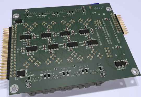
It ended up being a tight fit, but I was able to make it work on a 4-layer board within the same footprint of my main board, putting some components on the back side. (It may look like a bunch of empty space, but there's actually a lot going on running full RS232 with handshaking for 8 ports).
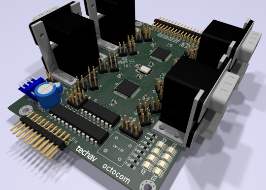
New problem. I had blown my budget for the project. As much as I love those stacked DE9 connectors, they're expensive. And there's no getting around the $10 pricetag for each of those quad UARTs. Even using parts on-hand where possible, I was looking at a hefty Mouser order.
[jbevren] suggested using ganged RJ45 connectors with the Cisco pinout instead of stacked DE9, to save space & cut costs. [Chartreuse] suggested buffering the TTL serial TX/RX signals to drive the LEDs that are frequently included on PCB-mount RJ45 connectors. Both great ideas. I was able to cut 20% off my parts order and add some nice diagnostic lights to the design.
Two weeks later, I received five new PCBs straight from China. I of course wasted no time setting into starting to assemble one.
I really set myself up for a challenge on this one. I learned to solder some 25 years ago and have done countless projects in that time. But I think this might be the most compact, most heavily populated, most surface mount board I've ever assembled myself. (There are 56 size 0805 (that's 2x1.2mm) capacitors alone!)


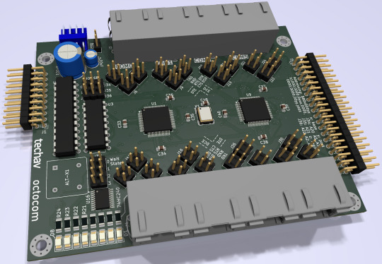
After a few hours soldering, I had enough assembled to test the first serial port. If the first port worked then the other three on that chip should work too, and there's a great chance the other chip would work as well.

And it did work! After some poking around with the oscilloscope to make sure nothing was amiss, I started up the computer and it ran just fine at 8MHz.
And at 16MHz.
And at 25MHz.
And at 32MHz.
And at 40MHz.
And almost at 50MHz!
Remember what I said about my timing graphs showing one wait state for 50MHz? The computer actually booted up and ran just fine at 50MHz. The problem was when I tried typing in a BASIC program certain letters were getting switched around, and try as I might, BASIC just refused to 'RQN' my program. It was pretty consistently losing bit 3, likely from that signal having to travel just a tiny bit farther than the others. A problem that will probably be resolved with an extra wait state.
Good enough for a first test! A few hours more and I finished assembling the card.

I did have some problems with cleaning up flux off the board, and I had to touch up a few weak solder joints, but so far everything seems to be working. I've updated my little multi-user kernel to run all 8 users from this new card and it's running stable at 40MHz.
I need to update my logic on the 22V10 to fix a bug in the wait state generator. I would love to see this thing actually running at 50MHz — a 25% overclock for the 40MHz CPU I am currently running. I also want to expand my little kernel program to add some new features like the ability to configure the console serial ports and maybe even load programs from disk.
I hope to bring this machine with a collection of terminals and modems this June to VCF Southwest 2025 for an interactive exhibit that can be dialed into from other exhibits at the show.
#wrap030#multi-user BASIC#EhBASIC#homebrew computer#motorola 68030#68030#mc68030#motorola 68k#vcfsw#vcfsw2025#Retrocomputing#rtc#retrotech crew
31 notes
·
View notes
Text


coming up with little PCBs to practice my surface mount soldering skills, this one is going to be a 2cm x 2cm target marker for warhammer. two tiny red LEDs and a switch on the front, and a coin cell battery on the back.
23 notes
·
View notes
Text
LED PCB Assembly
What is the LED Circuit Board assembly?
Generally, LED PCB assembly is considered to be a circuit board that has the LED components soldered to it. The LED is soldered to the printed circuit board and features a chip that creates the light as electrically connected. A thermal heat sink and a ceramic base are used to bond the chip. Not all the PCB products can be used in Led industry, as an LED PCB is easy to create a high volume of heat, but making it hard to cool with traditional methods. For this reason, metal core PCB is widely used in LED application because of their enhanced ability to dissipate heat, especially aluminum pcb is often used to fabricate PCB for LED lights.
We’ve had great LED PCB assembly experiences with top LED chips to brand such as Cree, Luxeon, Osram, Nichia, Lumileds, MLS, EVERLIGHT, Samsung, LG, Seoul., etc. PCB LED lights can be incorporated into numerous lighting applications due to their combination of excellent energy efficiency, low cost and maximum design flexibility.

Application of LED PCB Assembly
Hitechpcba serves customers in different industries, providing highly reliable and innovative LED PCBs for various applications:
• Horticulture light LED PCB Assembly
• LED controller PCB Assembly
• Computer LED display and indicators
• LED lights PCB Assembly for medical use
• Automotive LED PCBs Assembly include PCBs for brake lights and headlights
• Street lighting LED PCB Assembly
• Flashlights and camping accessories
• Traffic light PCB Assembly
• Commercial lighting LED PCB Assembly
LED PCB Assembly specification
Number of layers for LED PCB
These layers are made up of aluminum and magnesium, but now have Copper base material and Ceramic base materials for LED PCB industry, we can meet it.
Aluminum LED PCBs stand out among other PCBs because it has a good insulation characteristic and has a better machinery performance, the cheap cost is one important factor too.
Types of layers for LED PCB Assembly
Normally, the base layer is made using aluminum alloy metal.
This aluminum alloy substrate used in making the base makes it ideal for through-hole technology which transfers and dissipates heat.
A thermal insulation layer is made using some ceramic polymer which has good viscoelasticity characteristics.
It is highly heat resistant and protects the PCB against heat and mechanical stress.
The circuit layer, which is covered by a copper foil which can range from one to ten ounces.
LED Board type- single or in panel
Some boards are shapeless. For this reason, LED PCB panels are used. This reduces time, labor production and testing time.
Some LED PCB Assembly is done on a single board while others are done on panel boards.
LED PCB Assembly Process
Roughly, the PCBA process can be divided into theses phases: soldering paste printing > SMT (surface mounted technology) > reflow soldering > AOI (automated optical inspection)> THT (through-hole technology) > wave soldering > touch-up and cleaning > IC-programming > FCT (functional tests) > aging testing.
Below we show you the process.
Step1. Summarizing Project Information
Before contacting your supplier, make sure you have all the project information. Suppliers will need info following for quoting LED PCB assembly:
Gerber
BOM
LED PCB specification
Quotation quantity
Once you have gathered these information, you can contact us and request for a quote.
Of course, you can also provide the schematic, LED PCB Assembly pictures and even samples to us. The more details they have, the more accurate the supplier’s quotation will be.
Step2. Discussion and details about custom LED PCB Assembly
Different projects will have different requirements. Remember the special requirements mentioned in step 1? That’s going to be the focus of this session. Equipment and engineering capacity will not be identical between suppliers. Make sure your supplier has the equipment to produce and assemble major components and the corresponding testing capabilities.
For example, some vendors don’t have X-ray testing equipment, which means they can’t check the mount quality of BGA chips. Outsourcing this step will increase risk and cost. That’s what you don’t want.
Also, pay attention to time taken by the supplier to quote. Motherboards often contain hundreds or even thousands of components, and they are supplied by different manufacturers. To ensure the quality of the components, the supplier sourcing team will make multi-inquiries from these manufacturers or authorized suppliers to match customer’s requirement, which usually takes 2-3 business days, and even longer for some scarce chips. Therefore, if your project is complex and the supplier quotes you within few hours, double check with them.
Step3. Sample and feedback
After confirming the PI, the supplier will usually provide pre-production samples for your approval. At the same time, the supplier will also confirm with you the logistics plan of the bulk goods. Make sure they understand your shipping requirements, including details on packaging, customs clearance, taxes, etc.
For us to have a successful LED PCB Assembly process, its functions must be defined. Compliance requirement is defined to reduce the effect when components are selected.
The Bill of Materials is then generated from the information installed on the LED PCB.
All this information is used to assemble components which are identified from MOB to the LED PCB.
After that, the routing of traces is determined to each component, based on the size, shape of the circuit board and location of connectors.

Hitech Circuits is trusted by thousands of electronic engineers on their LED PCB assembly projects, from consumer, led bulb to precisely medical LED light, we can help you from the beginning of design stage; From commercial flood LED to industrial high power LED, from automotive LED to military LED, Venture is the perfect place for your LED PCB assembly requirement.
Hitech Circuits has been participated in hundreds and thousands of LED lighting projects, by providing LED PCB and also LED PCB assembly service.
Our LED PCB assembly had covered both ends of the Lighting Class LED size spectrum, assembling some of the largest (2 meter long boards) and some of the smallest LED Lighting applications which used in Medical Endoscopes.
LED PCB Assembly is very crucial in the current industrial development. Many electrical devises are being innovated and the old once being improved.
LED PCBs are useful due to the fact that they are made using materials that can transfer and dissipate heat. This characteristic increases device durability.
The world is changing with new technology, especially PCB technology that plays an essential role in the application of LED circuits. And the LED industry is taking advantage of this technology and growing faster.
As a full feature PCB solutions provider with more than a decade of experience, we're capable to provide LED PCB fabrication, components procurement and LED PCB assembly all under one roof. We can work with you to develop metal core PCB, aluminum circuit boards customized to your specific applications. We feature competitively priced PCBs made with standard FR-4 material that includes a thermal aluminum clad layer that will efficiently dissipate heat, keep all LED PCB components cool and significantly enhance the performance of your products.

LED pcb board, LED pcb assembly
LED with its advantages of high brightness, high efficiency, low heat, long life, is considered the most development potential in the 21st century lighting. In the market and policy driven by the rapid development of the domestic LED industry blowout has formed a relatively complete industrial chain, including the production of epitaxial wafers, chip preparation, packaging, integration, LED application. In 2010, China's LED industry scale, up from $ 827 billion in 2019 to 220 billion yuan, an annual growth rate of over 70%, higher than the 50% level of growth of the global LED lighting industry output value. Among them, the middle and lower reaches of the most complete industrial chain, accounting for 90% of the overall percentage of the GDP.Chinahas become the world's leading LED manufacturing base and important application market.
To further promote the technological innovation of the LED industry, construction and wide application of independent industry chain, China Electronic Appliance Corporation and industry associations to organize the theme of "Focus on the core energy LED Exhibition will be held November 9-11, 2010 in Shanghai International Expo Center and the 78th China Electronics Fair over the same period will be held will create from raw materials, epitaxial wafers, chip, LED bracket, LED accessories, LED packaging and supporting materials, the LED backlight upstream firm to the upstream and downstream enterprises of the display, lighting, landscaping, decorative lighting, traffic lights, automotive lighting, special lighting, to the equipment, instrumentation, software, finance, consulting and other service enterprises and technological exchanges and market trading platform, help the domestic industry sustained and healthy development, and promote the steady expansion of the LED application market.
In the LED industry chain upstream of the epitaxial wafers and LED chips accounted for 70% of the profits of the whole industry, and technology-intensive, capital-intensive, where the core technology of the LED. Well-known epitaxial wafer and chip production enterprises will be exhibited a number of energy-efficient, low heat, cost-effective LED products, many of whom have excellent products of international advanced level.
LED electronic pcb assembly manufacturing 100% Original LED Chip with one-stop in-house pcba services
3 notes
·
View notes
Text
Why Are Surface Mount Inductors Vital in Modern Electronics? A Complete Guide

Surface mount inductors have emerged as critical components in today’s compact and high-performance electronic devices. As the demand for miniaturization and efficiency continues to grow, these components offer a reliable solution for energy storage, filtering, and signal integrity. Whether you are designing consumer electronics, industrial systems, or automotive applications, understanding the role and advantages of surface mount inductors can significantly enhance your product development process.
What Are Surface Mount Inductors?
Surface mount inductors are passive electronic components designed to store energy in a magnetic field when electrical current flows through them. Unlike traditional through-hole inductors, surface mount variants are mounted directly onto the surface of a printed circuit board (PCB), enabling compact, low-profile, and automated assembly designs. These inductors are widely used for their efficient space utilization and high-frequency performance.
How Do Surface Mount Inductors Work?
The basic working principle of surface mount inductors is grounded in electromagnetic induction. When current passes through the coil inside the inductor, it creates a magnetic field. This field resists changes in the current, providing a filtering or energy storage function depending on the application.
Surface mount inductors are typically manufactured using a ferrite or powdered iron core surrounded by a coiled conductor. The magnetic properties of the core and the number of coil turns determine the inductance value. Their compact design allows them to perform reliably in dense circuit boards.
Where Are Surface Mount Inductors Used?
These inductors are essential in multiple sectors where space-saving components are crucial. Common applications include:
Smartphones, tablets, and laptops
Power supplies and DC-DC converters
Automotive electronic control units (ECUs)
RF and telecommunications systems
Medical and industrial instrumentation
LED lighting systems and IoT modules
Each of these areas requires high-performance signal integrity and energy efficiency, both of which are facilitated by surface mount inductors.
What Are the Key Benefits of Surface Mount Inductors?
Surface mount inductors provide a range of advantages for engineers and product designers. Their integration into compact electronics is particularly valuable in today’s market.
Enable miniaturized circuit design for compact devices
Support high-frequency operations with excellent performance
Reduce production time through automated pick-and-place mounting
Offer low DC resistance (DCR) for higher efficiency
Enhance electromagnetic compatibility (EMC) in sensitive circuits
Provide thermal stability in harsh environments
Available in a wide variety of inductance values and sizes
These benefits make them indispensable in both analog and digital electronic systems.
What Are the Different Types of Surface Mount Inductors?
The choice of surface mount inductor depends on the specific application and performance requirements. Key types include:
Wire-wound inductors: Known for high Q-factor and current handling capabilities, ideal for power applications.
Multilayer inductors: Offer compact size and are suitable for high-frequency filtering.
Thin-film inductors: Deliver precision and low-profile characteristics, often used in RF circuits.
Molded inductors: Provide strong mechanical durability, often used in automotive environments.
Each type has unique characteristics that influence its behavior in a circuit, and selecting the right one depends on factors such as frequency, current rating, and size constraints.
How to Choose the Right Surface Mount Inductor?
Selecting the right surface mount inductor for your application involves considering several important technical parameters:
Inductance (L): Measured in microhenries (µH) or nanohenries (nH), this value defines how much energy the inductor can store.
Current rating: Determines the maximum current the inductor can handle without saturating or overheating.
Saturation current: Indicates the point at which the inductor loses its inductive properties.
DC resistance (DCR): Lower DCR means better efficiency and less power loss.
Frequency range: Ensures compatibility with the intended signal or switching frequency.
Size and footprint: Must match the PCB layout and spatial constraints.
Understanding these parameters helps ensure optimal circuit performance, reliability, and compliance with regulatory standards.
Why Are Surface Mount Inductors Preferred Over Through-Hole Types?
While both surface mount and through-hole inductors serve similar electrical purposes, surface mount options are increasingly preferred in modern electronic assemblies. This shift is driven by:
Smaller package sizes suitable for compact PCBs
Better performance at higher frequencies
Faster, more cost-effective automated manufacturing
Improved thermal performance in high-density applications
Enhanced mechanical stability during vibration or movement
Surface mount technology enables the design of lightweight, efficient, and high-performance devices across various industries.
What Are the Trends in Surface Mount Inductor Technology?
As technology evolves, surface mount inductors continue to improve in performance, durability, and miniaturization. Key developments in this field include:
Use of advanced core materials for higher energy density
Lower EMI solutions to support 5G and wireless technologies
Integration with ICs and other passives for modular designs
Eco-friendly manufacturing with lead-free soldering
High-reliability solutions for automotive and aerospace sectors
These innovations make surface mount inductors a forward-looking solution for next-generation electronic products.
Where to Buy High-Quality Surface Mount Inductors?
Finding trusted suppliers is essential for securing reliable surface mount inductors. It’s important to source components from distributors that provide:
Comprehensive technical datasheets
RoHS-compliant and quality-certified components
Wide inventory of top brands and value options
Global shipping and responsive customer service
Compatibility with high-frequency and power electronics
Buyers and engineers should consider trusted electronic suppliers with extensive product listings and verified sourcing standards.
Conclusion
Surface mount inductors are indispensable building blocks of today’s advanced electronic systems. Their compact form factor, high-frequency capability, and reliable performance make them ideal for power conversion, signal conditioning, and EMI suppression tasks. By understanding how these components work, where they are used, and how to select the right one, engineers can unlock new possibilities in their designs. As innovation accelerates, surface mount inductors continue to play a central role in enabling smarter, smaller, and more efficient electronics.
0 notes
Text
Single Side PCB Manufacturers in India: Vaishnavi Electronics at the Forefront of Quality and Reliab
When it comes to cost-effective and reliable circuit board solutions, Single Side PCBs (Printed Circuit Boards) remain the go-to choice for a wide range of electronic applications. In India, where the demand for efficient and affordable electronics is rapidly growing, Vaishnavi Electronics has earned a reputation as a leading manufacturer of high-quality single side PCBs.
What is a Single Side PCB?
A Single Side PCB features a single layer of conductive material, typically copper, on one side of the board. All components are mounted on one surface, making it ideal for low-density, simple circuit designs.
These PCBs are widely used in:
LED lighting systems
Consumer electronics
Power supplies
Calculators and timers
Audio devices
Toys and gadgets
Thanks to their low cost, simple manufacturing, and easy maintenance, single side PCBs are often chosen for mass production and budget-conscious designs.
Why Choose Vaishnavi Electronics for Single Side PCBs?
As one of India’s trusted PCB manufacturers, Vaishnavi Electronics combines advanced manufacturing capabilities with a strong focus on customer needs. Here's why they stand out:
Decades of Expertise
With years of hands-on experience in PCB manufacturing, Vaishnavi Electronics brings deep technical knowledge and industry insights to every project.
High-Quality Standards
Each board goes through strict quality checks, ensuring excellent conductivity, precision drilling, and clean etching.
Cost-Effective Solutions
Vaishnavi offers competitive pricing without compromising on quality—perfect for small to large-scale production.
Custom Manufacturing
Whether you need PCBs in bulk or a custom design for a new prototype, their team can handle it all—from design consultation to final production.
Fast Turnaround
With streamlined manufacturing processes and in-house facilities, Vaishnavi ensures timely delivery, even for urgent orders.
Applications of Vaishnavi’s Single Side PCBs
Clients across India trust Vaishnavi Electronics for their wide application base:
LED Modules & Strips
Mobile Chargers & Adaptors
Switch Mode Power Supplies (SMPS)
Home Appliances
Consumer Audio Devices
Conclusion
If you're looking for a reliable, cost-effective, and experienced Single Side PCB manufacturer in India, Vaishnavi Electronics should be your first call. Their commitment to quality, delivery, and customer satisfaction makes them a standout choice in the Indian electronics manufacturing landscape.
Get in touch with Vaishnavi Electronics today for your next PCB requirement—experience precision, performance, and professionalism.
Visit:- https://www.vaishnavielectronics.co.in/single-side-pcb.html
0 notes
Text
ASROCK AMD Radeon RX 9060 XT Challenger 16GB OC GPUs

AMD Radeon RX 9060 XT Challenger Architecture
The ASROCK AMD Radeon RX 9060 XT Challenger 16GB OC graphics card handles 1440p gameplay faster with AMD's RDNA 4 architecture.
AMD RDNA 4 and AMD Radeon RX 9060 XT GPU power it. Next-generation design boosts rendering and performance with unified computing units with advanced ray tracing and AI accelerators.
The card includes 16GB of 128-bit Memory Bus-connected GDDR6 memory. The memory clock is 20 Gbps.
A 2700 MHz game clock and a 3290 MHz boost clock are on board.
Processors and Compute Units: The GPU includes 32 compute units, including third-generation RT and second-generation AI accelerators. Also included are 28 stream processors.
Essential Features and Technologies: ASROCK AMD Radeon RX 9060 XT Challenger
It supports OpenGL 4.6 and DirectX 12 Ultimate.
It supports PCI Express 5.0 via the x16 bus specification.
This lightning-fast gaming design targets improved 1440p performance.
Used AI-powered features and tech AMD FidelityFX Super Resolution 4's ML-powered upscaling and next-generation raytracing generate AI-enhanced graphics.
Used AMD products and supported AMD FidelityFX Super Resolution 4 (FSR 4), which game developers must integrate. AMD does not support FSR on other graphics cards.
AMD HYPR-RX is on Radeon RX 7000 Series GPUs and later. This technology enables AMD Fluid Motion Frames, Radeon Super Resolution, FSR, Radeon Anti-Lag, and Radeon Boost to work together.
Compatible with AMD Smart Access Memory technology, if OEM support is available, with AMD 500 Series or later motherboards with the latest BIOS, AMD Radeon RX 5000 Series GPUs, and Ryzen 3000 Series CPUs (certain models excluded).
An upgraded media engine improves streaming clarity.
Modern ultra-high refresh monitors can employ the updated Radiance Display Engine, which features DisplayPort 2.1a and HDMI 2.1b.
Featuring Future-Ready Technology and longevity.
For optimal AM5 platform performance with AMD Ryzen 9000 Series CPUs.
ASROCK AMD Radeon RX 9060 XT Challenger Resolution and Connectivity:
One HDMI 2.1b, three DisplayPort 2.1a. With a Digital Max Resolution of 7680×4320, it enables up to three screens for multi-viewing. Use HDCP.
Power:
The card needs a 550W PSU with one 8-pin power socket. Power delivery components like Dr. MOS, an integrated power stage for synchronous buck-set down voltage applications, improve thermal performance. It can produce 50A per phase continuously. Additionally, it uses Premium 90A Power Chokes, which have three times the saturation current and greater Vcore voltage than typical chokes.
Cooling system
Dual fans increase cooling efficiency and balance performance and silence. Striped Axial Fans increase airflow with their blade stripe construction and bottom polishing surface. The 0dB Silent Cooling feature turns off the fans at low temperatures for quiet and on when the temperature rises. Cooling includes Ultra-fit and consolidated heatpipes to maximise GPU baseplate contact and heat dissipation.
High-density metal welding isolates pipes and stacked fins, improving heat dissipation. Nano Thermal Paste maximises heat transfer and closes contact gaps. Components heat the heatsink via reliable thermal pads. To protect the GPU die and maximise cooler mounting pressure for thermal efficiency, precise screw torque is employed during construction.
ASROCK AMD Radeon RX 9060 XT Challenger PCB and Hardware:
A sleek metal backplate avoids PCB bending and increases cooling using thermal pads. An LED On/Off Switch turns on or off LED indicators for decoration. The PCB architecture includes a 2 oz copper PCB for lower temperatures and energy efficiency, a matte black PCB with an intriguing colour scheme, and a high density glass fabric PCB to fill layer gaps and prevent humidity-induced electrical shorts.
AMD Radeon RX 9060 XT Challenger Software
User-friendly AMD Software Adrenaline Edition controls performance with trustworthy drivers, real-time AI-powered support, and one-click AMD HYPR-RX optimisation. This software improves gameplay with higher frame rates, less lag, and sharper graphics.
Dimensions and Weight:
Card weighs 645 g and dimensions 249 x 132 x 41 mm.
Price and Availability
The ASRock AMD Radeon RX 9060 XT Challenger 16GB OC graphics card will launch internationally on June 5, 2025, for $349 USD.
#AMDRadeonRX9060XT#AMDRadeonRX9060#RadeonRX9060XT#RX9060XTGPU#AMDRadeonRX9060XTChallenger16GBOC#ASRockAMDRadeonRX9060XT#technology#technews#technologynews#news#govindhtech
0 notes
Text
Choosing the Right PCB Material: A Comprehensive Guide | PCB Power

Choosing the Right Printed Circuit Board Material: A Comprehensive Guide
The choice of materials commonly used for the fabrication of the PCB is extremely important in determining the quality of it. The selection of PCB base material can impact electrical properties, thermal and mechanical behaviour, and reliability of the final product. In this blog, we will learn about the printed circuit board materials which are available to the buyers and their characteristics.
Common Types of PCB Materials
A list of the most common printed circuit board material is given below:
1. FR-4
FR-4 is the most common substrate material for making multi-layer printed circuit boards. It is a fibreglass-epoxy composite, with high dielectric strength. The material FR-4 can retain its stability up to the temperature of 130°C (266°F). It is used in consumer electronics, industrial control, telecommunications and other general application gadgets.
2. Polyimide
Polyimide is famous for its heat resistance and flexibility characteristics. It is commonly applied to flexible PCBs, where the board can be bent or folded. For example, in the case of a smartphone design. Polyimide can work up to a temperature of 260°C (500 °F). It is appropriate for aerospace, automobile, and medical devices where high performance is required.
3. Metal Core PCBs
Metal core PCBs are designed with a metal base material, often aluminum or copper. It offers five times better heat dissipation than FR-4 boards. These boards are popular in areas of heat dissipation which may include LED lighting and power electronics. Metal core PCBs have better thermal management under thermal loads.
4. Rogers Materials
Rogers Corporation produces a range of high-frequency materials that are suitable for advanced applications requiring precise electrical performance. Rogers materials provide low-loss characteristics and stable dielectric constants across varying frequencies.
They are used in telecommunications, aerospace, and military applications.
5. Taconic TSM-DS TLY-5 & DS3
Taconic TSM-DS TLY-5 and DS3 are specialized PCB materials intended for high-frequency applications. They are characterized by low dielectric constants and loss tangents, which keep the signal integrity at RF and microwave frequencies. Taconic materials are used in telecommunications and automotive radar.
Factors to Consider While Choosing PCB Materials
These are some factors one must consider before selecting the material for a printed circuit board:
1. Material Type and Properties
The choice of PCB material significantly impacts its functionality and reliability. Understanding the properties of the materials, such as dielectric constant (Dk), loss tangent (Df), and thermal expansion coefficient (CTE), is important.
2. Thermal Management
If there is heat involved, then thermal performance is very important, especially for high-power applications. The main thermal properties to study are as follows.
Glass Transition Temperature (Tg): At this temperature, the material would go from being a rigid state to more flexible. Thus, higher Tg materials are better to be used at high temperatures.
Decomposition Temperature (Td): It is the temperature at which the material will begin decomposing. Better indications under very difficult conditions are seen in higher Td.
3. Manufacturing Process Compatibility
The chosen material should also correspond to the manufacturing method employed, i.e., through-hole or surface mount technology (SMT). For example, SMT relies on FR-4 for favourable drillability, while flexible PCBs need materials such as polyimide, which don't crack during bending.
4. Environmental Considerations
Always evaluate the PCB's operational condition since humidity, temperature rise and fall, and exposure to chemicals influence the selection process of materials. Ensure the selected materials can withstand these conditions without degrading.
5. Frequency Range
In an instance where high-frequency signals are involved, it is critical to select materials that have low dielectric loss. High-speed PCBs may require special material under this.
Conclusion
Choose the right printed circuit board material to get the best result in the electronic designs. Designers must know about the properties of various materials such as FR-4, polyimide, PTFE, metal core, and Rogers to satisfy the needs of the projects. Electrical behavior, thermal properties, mechanical strength, cost ,and feasibility of PCB fabrication during manufacturing will help you decide which material is most suitable for your particular project.
At PCB Power, we manufacture high-quality printed circuit boards crafted from a variety of materials, including FR-4, polyimide, and metal core. Whether you are looking for prototype circuit boards or need them in volume, PCB Power can be your trusted partner
Contact our team of experts to discuss your requirements.
Know More: https://www.pcbpower.us/blog/choosing-right-pcb-material-guide
0 notes
Text
First Seal India: Premier Thermal Conductive Silicone Sealant Manufacturer
In the realm of electronics and electrical applications, effective heat management is paramount. First Seal India, based in Ahmedabad, Gujarat, stands at the forefront of providing high-quality thermal conductive silicone sealants designed to meet the stringent demands of modern industries.
About First Seal India
Established with a commitment to innovation and quality, First Seal India specializes in the production and supply of advanced thermal management solutions. Their flagship product, the FS-7576 Thermal Conductive Silicone Sealant, exemplifies their dedication to excellence in the field.
Product Overview: FS-7576 Thermal Conductive Silicone Sealant
The FS-7576 is a one-component, room-temperature vulcanizing (RTV) silicone sealant formulated to deliver exceptional thermal conductivity and reliable adhesion. Key features include:
Thermal Conductivity: 1.0 ± 0.2 W/m·K
Density: 1.6 ± 0.1 g/ml
Shore A Hardness: 30
Breakdown Voltage: 10.0 kV/mm
Operating Temperature Range: -40°C to 180°C
Maximum Temperature Resistance: Up to 250°C
This sealant is ideal for applications requiring efficient heat dissipation and secure bonding without the need for mechanical fasteners.
Applications
The FS-7576 sealant is widely utilized in various sectors, including:
Power Supplies and Chargers: For secure bonding and heat conduction.
LED Lighting: Ensures effective thermal management in LED lamp radiators.
Printed Circuit Boards (PCBs): Facilitates heat conduction for surface-mount devices (SMDs).
Electronic and Electrical Components: Provides bonding and heat conduction solutions.
Packaging Options
To cater to diverse industrial needs, First Seal India offers the FS-7576 sealant in various packaging sizes:
50 ml/tube (200 tubes/box)
100 ml/tube (120 tubes/box)
300 ml/tube (25 tubes/box)
2600 ml/tube (4 tubes/box)
Customized special packaging available upon request
Storage and Handling
For optimal performance, it is recommended to store the FS-7576 sealant in a dry, cool place, avoiding exposure to sunlight and moisture. The product has a shelf life of six months when stored at 25°C.
Contact Information
For more details or to place an order, please contact:
Phone: +91-63531 35337
Email: [email protected]
Website: www.firstsealindia.com
First Seal India's commitment to quality and innovation ensures that their thermal conductive silicone sealants meet the evolving needs of industries requiring efficient heat management solutions.
0 notes
Text
Failure Mode Analysis of Metal Push Button Switches and Field Case Reviews

Introduction
Metal push button switches, despite their robust design, are still subject to various failure modes in practical applications. These failures not only reduce product reliability but also lead to maintenance costs and safety issues in customer sites. This article analyzes common failure modes of metal push button switches—such as contact arcing, button jamming, LED failure, and seal degradation—and reviews real customer cases to provide targeted design optimization suggestions.
1. Common Failure Modes and Root Cause Analysis
1.1 Contact Arcing and Wear
Phenomenon: After long-term use, switch contact resistance increases, even resulting in failure to conduct.
Cause:
High inrush current without arc suppression.
Inadequate contact material (e.g., pure copper without plating).
High operating voltage or inductive load.
Optimization:
Use silver-nickel or gold-plated contacts for high current reliability.
Add arc suppression components (RC snubber or MOV).
Reinforce spring force to ensure contact pressure.
1.2 Button Jamming
Phenomenon: The button becomes stuck in the pressed position and does not rebound.
Cause:
Debris ingress due to poor sealing.
Deformation of spring plate.
Excessive wear on plastic guide sleeve.
Optimization:
Use dustproof and waterproof structures (e.g., IP67 design).
Reinforce spring plate material and shape (e.g., double-curvature dome).
Use self-lubricating plastic or metal guide sleeves.
1.3 LED or Light Ring Failure
Phenomenon: LED does not light up or flickers after a period of use.
Cause:
LED solder joint fracture due to vibration.
Electrostatic breakdown or surge.
Moisture ingress leading to corrosion.
Optimization:
Use flexible PCB and reinforcement glue for LED solder joints.
Add TVS protection to the LED circuit.
Improve potting and waterproof design of light ring.
1.4 Seal Failure (IP Degradation)
Phenomenon: Moisture ingress, fogging inside switch, corrosion.
Cause:
Poor sealing design (e.g., thin O-ring, low contact pressure).
Material aging (e.g., silicone rubber hardening).
Incorrect installation causing compression loss.
Optimization:
Use high-performance fluorosilicone O-rings.
Design mechanical structures that maintain sealing pressure under thermal expansion.
Add secondary sealing like glue filling or ultrasonic welding.
2. Case Studies from Customer Sites
Case A: Food Processing Machine Button Fails after 3 Months
Problem: Button became sticky and unreliable; LED flickered.
Analysis: High humidity and oil vapor caused internal corrosion and solder failure.
Solution: Upgraded to IP68 switch with epoxy-sealed LED and food-grade silicone sealing ring. After redesign, no failure in 6-month follow-up.
Case B: Elevator Call Panel Button Lost Tactile Feedback
Problem: Users reported button was soft and unresponsive.
Analysis: Long-term mechanical fatigue led to spring plate deformation.
Solution: Changed to double-spring structure (coil + dome), added fatigue life test in production. Mechanical cycles improved from 300,000 to 1.2 million.
Case C: Industrial Panel with Intermittent Contact
Problem: Switch signal occasionally failed.
Analysis: Contact surface oxidation due to prolonged storage and lack of current load.
Solution: Switched to gold-plated contacts, added low-current self-cleaning pulse during power-on to ensure reliability.
3. Proactive Design Recommendations
Reliability testing: Include high/low temperature cycling, salt spray, vibration test.
Redundancy: In critical environments, use redundant contacts or signal confirmation circuits.
Installation training: Guide customers to use correct torque and mounting methods to avoid sealing damage.
Conclusion
By thoroughly understanding the failure modes of metal push button switches and drawing lessons from field failures, we can implement targeted design optimizations to improve product reliability. This not only enhances user satisfaction but also reduces after-sales maintenance costs, building long-term trust with B2B clients.
en.dghongju.com
0 notes
Text
PCB Components: Active & Interactive – A Deep Dive Into Buttons, Switches, And LED Integration
Printed Circuit Boards (PCBS) are the foundation of modern electronic devices, and the components mounted on them determine the function, interactivity, and performance of the final product. Among these components, those that add user interaction and visual feedback are especially important. In this article, we explore key PCB components that are both active and interactive, including LED light components, PCB buttons, touch buttons, PCB switches, and circuit board switches.
The Role of Active and Interactive Components in PCBS
While resistors, capacitors, and microcontrollers form the brain and nervous system of a circuit, interactive components are the parts users directly engage with. These include input and output elements like switches, buttons, and LEDS that provide feedback or control functionality. Their design, placement, and integration into the PCB layout determine the user experience and overall product usability.
LED Light Components – Visual Feedback and Functionality
LED light components are perhaps the most widely used visual indicators in electronics. These can signal power status, indicate processing states, or serve as alerts. In modern consumer electronics, RGB LEDS are often integrated to offer multi-colour feedback in a single package. Their compact form makes them ideal for PCB integration. Designers typically use surface-mount or through-hole LEDS depending on the size constraints and the manufacturing process.
LEDs can also be interactive. For example, when integrated with a light sensor or a touch button, an LED can respond to environmental changes or user actions, enhancing the device's intuitive feel.
PCB Buttons – Tactile and Durable
A PCB button refers to a mechanical push-button mounted directly onto the circuit board. These are common in devices requiring tactile feedback, such as remote controls, handheld gadgets, and industrial interfaces. Typically made of conductive rubber or metal domes, PCB buttons close a circuit when pressed, sending a signal to the controller.
Their mechanical durability, ease of replacement, and firm tactile response make them ideal for products that demand consistent user interaction. Proper design and spacing are crucial to ensure longevity and reliability.
Touch Buttons – Sleek and Modern
Touch buttons are a modern alternative to mechanical buttons. They use capacitive or resistive sensing to detect a user’s finger. These buttons provide a seamless, flat surface and are often used in devices like microwaves, induction cookers, and smartphones. Because they have no moving parts, they tend to last longer and are more resistant to dust and moisture.
Touch buttons are typically implemented by adding a conductive pad on the PCB, connected to a capacitive sensing IC. With appropriate firmware, touch sensitivity can be fine-tuned for better performance across different environments.
PCB Switches – Controlling Power and Modes
PCB switches refer to various types of toggle, slide, or rocker switches mounted on a circuit board. They allow users to change operating modes, turn devices on or off, or control specific functions. These switches are ideal for applications where physical state changes are necessary and must be visually verified (e.g., ON/OFF positions).
From DIP switches used in older hardware settings to modern micro slide switches in wearable tech, the variety of PCB switches allows for wide application flexibility.
Circuit Board Switch – A Broad Term with Specific Use
The term circuit board switch is often used interchangeably with PCB switches, but it can also refer to any electrical switch mounted on a board. This includes everything from tactile buttons to rotary encoders. These switches play a crucial role in routing electrical signals and enabling user control.
Summing It Up
Understanding and integrating active and interactive PCB components like LED light components, PCB buttons, touch buttons, PCB switches, and circuit board switches is essential for creating intuitive and functional electronic devices. Designers must consider user experience, durability, and responsiveness when selecting these elements. As technology continues to advance, these interactive components will evolve to provide smarter, sleeker, and more seamless user interfaces.
0 notes
Text
Ceramic PCB Assembly: Unlocking Advanced Performance in Electronics
As electronics continue to push the boundaries of speed, power, and miniaturization, ceramic PCB assembly has emerged as a crucial technology. Combining exceptional material properties with precise assembly techniques, ceramic PCBs are increasingly used in industries that demand reliability and superior performance.
What is Ceramic PCB Assembly?
Ceramic PCB assembly refers to the process of mounting and soldering electronic components onto a ceramic-based printed circuit board. Unlike traditional fiberglass (FR4) boards, ceramic PCBs use substrates like alumina (Al₂O₃), aluminum nitride (AlN), or beryllium oxide, offering remarkable thermal conductivity, electrical insulation, and mechanical strength.
Why Choose Ceramic PCB Assembly?
1. Excellent Heat Management Ceramic PCBs can handle extreme temperatures and high power loads without warping or losing performance. This makes them ideal for LED modules, power electronics, and automotive systems where heat buildup is a critical concern.
2. Superior Electrical Performance With low dielectric constants and high insulation resistance, ceramic substrates minimize signal loss and crosstalk, making them perfect for high-frequency applications, including 5G devices, radar systems, and aerospace electronics.
3. Durability and Longevity Ceramic PCBs are highly resistant to moisture, chemicals, and mechanical stress. When assembled properly, they offer outstanding longevity and reliability, even in harsh environments.
The Ceramic Assembly Process
Ceramic PCB assembly involves several specialized steps:
Surface preparation: Ensures the ceramic surface is clean and ready for soldering.
Component placement: Uses precision machines to position small or complex components accurately.
Soldering techniques: Because ceramics don’t expand like FR4, techniques like epoxy bonding, low-temperature soldering, or silver sintering are often used.
Inspection and testing: Final products undergo thorough quality control to ensure electrical and mechanical integrity.
Applications of Ceramic PCB Assembly
Ceramic PCBs are widely used in LED lighting, medical devices, power converters, satellite systems, and automotive electronics. Their ability to perform under demanding conditions makes them a preferred choice for cutting-edge projects.
Final Thoughts
Ceramic PCB assembly plays a vital role in modern electronics, offering unmatched thermal and electrical advantages. Ceramic PCBs will continue to unlock new possibilities as technology evolves, driving innovation across industries.
0 notes
Text
DAEJOO : A Trusted Name in Marine & Industrial Automation Explore the Full Range at Aeliya Marine
In the constantly changing world of ocean and industrial automation, few names have withstood the test of time, providing precision, reliability, and confidence. One of them is DAEJOO, known around the globe for its cutting-edge engineering and high-reliability parts. Be it a business vessel traveling open seas or an assembly line that cannot pay the luxury of a second of downtime, DAEJOO’s automation components guarantee performance sans compromise.
At Aeliya Marine Tech, we are pleased to showcase a handpicked range of original DAEJOO products designed to satisfy marine engineers as well as industrial specialists. Ranging from hard-to-find PCBs to reliable relay units and control modules, our DAEJOO product portfolio is extensive, quality-approved, and ready to ship across the globe.
About DAEJOO Engineering Excellence You Can Rely On
DAEJOO Industrial Co., Ltd., based in South Korea, is a renowned producer of marine-grade electrical and automation components. With an emphasis on high-performance circuit design, interface reliability, and system safety, DAEJOO has emerged as the go-to option for shipyards, offshore platforms, naval maintenance teams, and industrial control engineers globally.
The mission of the company has ever been simple: to produce parts that endure, even in extreme environments. Those are products resistant to high humidity, saltwater corrosion, voltage spikes, and temperature extremes conditions prevalent both in marine and heavy industrial applications.
Discover the DAEJOO Product Categories at Aeliya Marine
Let’s start with some of the fundamental product categories found on our website under the DAEJOO banner:
1. Control Modules
DAEJOO’s control modules are the workhorse of a wide range of shipboard and industrial automation applications. With sturdy build quality and reliable interfacing logic, the modules provide the seamless execution of commands and control signals on any automation network.
Standard features :
High insulation resistance
DIN-rail mounting with compact dimensions
LED indication of diagnostic status
Fail-safe options
2. Interface Boards & PCBs
DAEJOO Printed Circuit Boards (PCBs) are designed to provide precise signal control and voltage regulation. They find application in main control panels, sensor systems, navigation controls, and motor interface units.
Regardless of whether you’re replacing a defective board or modernizing an old system, these PCBs provide :
Consistent copper trace paths
Built-in EMI protection
Components with surface-mount or through-hole
Clear part labeling and revision control
3. Relays & Timer Units
DAEJOO relays are ideal for timed switching, fault detection, and manual override systems applications. Their small sizes and conventional pin configurations simplify integration.
Benefits are:
Low power coil operation
Long mechanical and electrical life
High surge withstand capacity
ISO and IEC compliance
4. Power Supply Units & I/O Modules
In both factory and marine systems, power stability and input/output control are essential. DAEJOO’s power supply units provide stable voltage output with protective features such as overcurrent and thermal shutdown.
At the same time, their I/O modules provide :
Modular expansion
Easy plug-and-play connections
Flexible voltage and signal support (DC/AC)
Noise-filtering for reliable communication
Why Purchase DAEJOO from Aeliya Marine Tech?
At Aeliya Marine, we’re not merely product resellers we’re technical allies. Our mission is to assist engineers and purchasing teams in discovering genuine, tried, and deployable components, particularly when time and dependability are most critical.
Here’s why our customers worldwide have confidence in us:
1. Authenticated Genuine Parts
We buy directly from trusted networks so that each DAEJOO component is genuine and performance-verified. No fakes, no inferior substitutes only the original.
2. Complete Specifications & Images
We offer detailed specs, model codes, datasheets (where necessary), and hi-res images so you can be sure of what you’re getting.
3. Fast Dispatch & Global Shipping
Want it ASAP? We facilitate quick and trusted shipping to world ports and cities. Our logistics division in Mumbai is capable of processing express overseas orders.
4. Competitive Prices & Bulk Rate Discounts
Competitive prices and discounts for multi-unit purchases make Aeliya Marine the intelligent choice for business and solo technicians.
5. Professional Customer Support
We are here to assist you with selecting the proper part, confirming compatibility, and monitoring your order. Need some help with installation or wiring schematics? No worries.
Hot DAEJOO Products Available on Our Site
Below are some of our top customers’ favorites from our new DAEJOO range :
DAEJOO Interface Card DJ-2310 Series : Applied in ship automation consoles
DAEJOO DJR-105 Relay Unit : Suitable for motor protection and emergency override
DAEJOO Terminal Block DJT Series : Corrosion-proof and compact
DAEJOO Control Unit DJK-218 : Multi-channel logic control of automation systems
All of these products come with technical descriptions and pictures to assist you in identifying them properly.
Applications of DAEJOO Products
DAEJOO components are engineered to withstand the demanding requirements of various industries, including:
Marine Applications :
Engine Room Automation
Navigation Control Panels
Bridge Monitoring Systems
Alarm & Safety Circuits
Industrial Applications :
PLC-Based Automation
Machine Tool Controls
Conveyor System Integration
Power Distribution Panels
The versatility of DAEJOO components ensures that they are the first choice for engineers in various fields.
The Aeliya Marine Advantage : More Than Just a Vendor
When you buy from Aeliya Marine Tech, you’re buying from an organization that shares your sense of urgency and technical sophistication. We deal with professionals from shipyards, offshore facilities, steelworks, cement factories, and automakers who rely on us for:
Rare to find obsolete spares
System-compatible substitutes
Thoroughly inspected used & refurbished parts
Open service, from inquiry through delivery
We also assist customers in locating similar or compatible models when the original DAEJOO product is not available preventing downtime and saving money.
Wrapping Up : Reliable Technology for Demanding Systems
With DAEJOO’s established reliability and Aeliya Marine’s rapid response service, you can flow your maintenance, repair, or system upgrade project with total peace of mind. Whether you are upgrading your control room, renovating an ageing PCB, or refining a relay-based system, our DAEJOO series is designed to assist you to deliver results.
Ready to explore?
Click Here To View The Complete Daejoo products Collection
#industrial equipment#automation#industrialautomation#industrial spare parts#industrial and marine automation#marine automation#industrial automation#pcb#amplifier#meter#deajoo
0 notes
Text
LED is the abbreviation of light emitting diode (Light Emitting Diode, LED),
LED is the abbreviation of light emitting diode (Light Emitting Diode, LED), also known as light emitting diode, this semiconductor element is generally used as an indicator light, a display panel, it can not only efficiently directly convert electrical energy into light energy, but also has up to tens of thousands of hours~ 100,000 hours of service life, while not as fragile as traditional bulbs, and can save electricity and other advantages.
However, no matter what kind of LED, it needs to be reasonably designed for different types of packaging, because only the packaged ones can become end point products and be put into practical application.
1. Why should LEDs be encapsulated?
The function of LED packaging is to connect the outer leads to the electrodes of the LED chip, which not only protects the LED chip, but also improves the luminous efficiency. Therefore, LED packaging not only completes the output of electrical signals, but also protects the normal operation of the die and outputs visible light. It can be seen that LED packaging has both electrical parameters and optical parameters design and technical requirements, which is not a simple task.
2. LED packaging equipment
Due to the high requirements of LED packaging, whether it is an in-line LED or a patch LED, a high-precision solid crystal machine must be used, because whether the position of the LED chip into the package is accurate will directly affect the luminous efficiency of the whole package device. If the position of the chip in the reflective cup is deviated, the light cannot be completely reflected, which directly affects the brightness of the LED. However, with an advanced PR System (pre-image recognition system) solid crystal machine, the LED chip can still be precisely soldered to the predetermined position regardless of the quality of the lead frame.
3. LED package form
According to different applications, different external dimensions, heat dissipation schemes and luminous effects. LED packaging forms are various. At present, LEDs are mainly classified according to packaging forms: Lamp-LED, TOP-LED, Side-LED, SMD-LED, High-Power-LED, Flip Chip-LED, etc
Lamp-LED (Vertical LED)
The early appearance of Lamp-LED is in-line LED, which is packaged in the form of potting. The process of potting is to inject liquid epoxy resin into the LED molding cavity, then insert a pressure-welded LED bracket, put it in an oven to let the epoxy resin cure, and then detach the LED from the cavity and form it immediately. Due to the relatively simple manufacturing process and low cost, it has a high market share.
SMD-LED (surface adhesive LED)
SMD LED is attached to the surface of the circuit board, suitable for SMT processing, reflow soldering, which solves the problems of brightness, viewing angle, flatness, reliability, consistency, etc., using lighter PCB board and reflective layer materials. After improvement, the heavier carbon steel material pins of the in-line LED are removed, so that the display reflective layer needs to be filled with less epoxy resin, the purpose is to reduce the size and weight. In this way, the surface mount LED can easily reduce the weight of the product by half, ultimately making the application more perfect.
Side-LED (side-emitting LED)
At present, another key point of LED packaging is the side-emitting package. If you want to use LED as the backlight source of LCD (liquid crystal display), the side-emitting light of LED needs to be the same as the surface-emitting light, so that the LCD backlight emits evenly. Although the design of the lead frame can also achieve the purpose of side-emitting light, the heat dissipation effect is not good. However, Lumileds invented the design of the mirror, which uses the principle of the mirror to emit side light, and successfully applies high-power LEDs to large-size LCD backlight modules.
TOP-LED (top-emitting LED)
The top light-emitting LED is a relatively common SMD light-emitting diode. Mainly used in backlights and status indicators in multi-function ultra-thin mobile phones and PDAs.
High-Power-LED (High Power LED)
In order to obtain high-power and high-brightness LED light sources, manufacturers have developed high-power LED chip and package designs. At present, LED packages that can withstand several W of power have appeared. For example, the package structure of Norlux series high-power LEDs is a multi-chip combination with a hexagonal aluminum plate as a base (making it non-conductive). The base diameter is 31.75mm, and the light-emitting region is located in its center. The diameter is about (0.375 × 25.4) mm, which can accommodate 40 LED dies. The aluminum plate is used as a heat sink at the same time. This package adopts a conventional die high-density combination package, which has high luminous efficiency, low thermal resistance, and high light output power under high current. It is also a promising LED solid light source.
It can be seen that the thermal characteristics of power LED directly affect the operating temperature, luminous efficiency, luminous wavelength, and service life of LED, etc. Therefore, the packaging design and manufacturing technology of power LED chips are even more important.
Flip Chip-LED (Clad Crystal LED)
The LED overlay packaging structure is basically made with a plurality of perforations in the PCB, and each perforation on one side of the substrate is provided with two different areas of conductive material that are open to each other, and the conductive material is tiled on the substrate. On the surface, there are a plurality of unpackaged LED chips placed at each perforation on the side of the conductive material. The positive and negative contacts of a single LED chip are connected with the conductive material on the substrate surface by solder balls, respectively, and on the surface of the side of the plurality of LED chips facing the perforation, there is a transparent sealant. The sealant is in the shape of a half sphere and is located at each perforation. It belongs to flip-chip light emitting diodes.
conclusion
According to the principle of solid-state light-emitting physics, the luminous efficiency of LED is approximately 100%. Therefore, LED is known as a new light source in the 21st century, and is expected to become the fourth generation light source after incandescent lamps, fluorescent lamps, and high-intensity gas discharge lamps. Looking to the future, manufacturers will definitely place high-power and high-brightness LEDs in a prominent development position. The substrate, epitaxy, chip, packaging, and application in the LED industry chain need to be jointly developed and cultivated by multiple parties. Packaging is the upper and lower parts of the industry chain, and requires great attention and attention from everyone.
0 notes