#PCBAssemblyservices
Explore tagged Tumblr posts
Visit Tumblr Blog
Explore Tumblr blogs with no restrictions, modern design and the best experience.
Last Seen Tumblr Blogs


Fun Fact
Mobile Tumblr US users spend an average of 4.04 minutes per session on the app.
Text
https://intellisenseapps.livepositively.com/driving-innovation-through-expert-pcb-design-services/
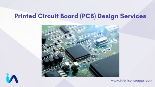
#PCBDesign#PrintedCircuitBoard#PCBLayoutDesign#PCBManufacturing#PCBAssembly#ElectronicsDesign#PCBDesignServices#PCBPrototyping#PCBAssemblyServices#CircuitDesign#EmbeddedSystems#ElectronicsEngineering#IoTDesign#PCBPrototypingServices
0 notes
Text
Crafting the Future: Aimtron's Mastery in PCB Assembly and Electronics Manufacturing

In today's fast-paced technological landscape, the demand for high-quality PCB Assembly and Electronics Manufacturing is greater than ever. As industries evolve, the need for precision, reliability, and efficiency in electronic components continues to shape the future. Aimtron Electronics has established itself as a leader in PCB Assembly solutions, seamlessly integrating ESDM (Electronic System Design & Manufacturing) expertise to drive innovation.
The Backbone of Electronics Manufacturing: PCB Assembly
At the heart of every electronic device lies a printed circuit board (PCB), the foundation for connectivity and performance. A robust PCB Assembly process ensures seamless operation, longevity, and efficiency. The key stages of PCB Assembly services include:
Component Selection & Sourcing: Procuring premium electronic components for durability.
Surface Mount Technology (SMT): High-precision component placement using automated systems.
Through-Hole Assembly: Strong, reliable connections for demanding applications.
Testing & Quality Control: Rigorous inspections to eliminate defects and ensure peak performance.
With cutting-edge PCB Assembly solutions, manufacturers like Aimtron Electronics empower businesses with reliable and cost-effective technology.
ESDM: Elevating Electronics Manufacturing
Electronic System Design & Manufacturing (ESDM) goes beyond assembling PCBs—it involves designing, prototyping, and producing entire electronic systems. High-quality ESDM solutions optimize:
Efficiency: Streamlined workflows for faster production.
Customization: Tailored designs for industry-specific applications.
Innovation: Advanced engineering for next-generation electronics.
Combining PCB Assembly and ESDM expertise results in high-performance, scalable solutions that meet the demands of modern industries.
Aimtron Electronics: Leading the Charge in PCB Assembly & ESDM
With decades of experience, Aimtron Electronics has set new standards in electronics manufacturing, ensuring quality, reliability, and innovation. Their comprehensive approach includes:
Advanced Manufacturing Facilities: Cutting-edge technology for precision assembly.
Comprehensive Testing Protocols: Stringent quality control for defect-free products.
Custom Solutions: Industry-specific designs for optimized performance.
Sustainability & Efficiency: Eco-friendly production methods for responsible manufacturing.
The Future of Electronics Manufacturing
The fusion of PCB Assembly and ESDM solutions is shaping the future of electronics manufacturing. As industries transition towards smarter, more efficient technologies, Aimtron Electronics continues to drive innovation, crafting the future with mastery in PCB Assembly and ESDM.
Looking for expert PCB Assembly and ESDM solutions? Aimtron Electronics is your trusted partner in delivering cutting-edge electronics manufacturing that stands the test of time.
0 notes
Text
Understanding PCB Assembly Services | A Key to Your Electronics Manufacturing Success | Lion Circuits
In the ever-evolving landscape of electronics manufacturing, PCB assembly services play a pivotal role in bringing innovative products to life. As the backbone of modern electronic devices, printed circuit boards (PCBs) are crucial for ensuring that everything functions seamlessly. At Lion Circuits, we specialize in providing top-tier PCB assembly solutions tailored to meet the diverse needs of our clients.
What Are PCB Assembly Services?
PCB assembly services involve the process of connecting various electronic components to a printed circuit board. This includes soldering components onto the board, testing the assembled boards, and preparing them for delivery. The process can vary based on the complexity of the design, the type of components used, and the specific requirements of the end product.
Types of PCB Assembly Services
Surface Mount Technology (SMT): SMT is widely used in modern electronics due to its ability to accommodate smaller components and higher circuit densities. Our PCB assembly services include advanced SMT techniques, ensuring that your products are both compact and efficient.
Through-Hole Technology (THT): For certain applications, especially those requiring more robust connections, through-hole technology remains essential. Our team is experienced in this traditional method, providing a complete range of assembly options.
Mixed Technology Assembly: Many projects require a combination of SMT and THT. Our expertise in mixed technology assembly ensures that we can accommodate diverse component types on a single PCB, offering flexibility and efficiency.
Prototype Assembly: If you're developing a new product, our prototype assembly services can help you test and refine your design. This stage is critical for identifying potential issues before mass production, saving both time and resources.
Volume Production: Once your prototype is finalized, we offer scalable PCB assembly services for high-volume production runs. Our state-of-the-art facilities ensure that we can meet your production demands while maintaining high quality and consistency.
Why Choose Professional PCB Assembly Services?
Opting for professional PCB assembly services provides several advantages:
Expertise: Our team possesses extensive knowledge in PCB design and assembly, ensuring that your products meet industry standards and specifications.
Quality Control: We implement rigorous testing and quality assurance processes to guarantee that each PCB meets the highest quality standards.
Cost-Effectiveness: By leveraging our advanced technology and expertise, you can reduce manufacturing costs and improve efficiency.
Time Savings: Outsourcing your PCB assembly allows you to focus on other critical areas of your business, such as product development and marketing.
Conclusion
Investing in reliable PCB assembly services is essential for the success of your electronics projects. At Lion Circuits, we are committed to delivering high-quality, efficient, and scalable solutions tailored to your specific needs. Whether you require prototype assembly or high-volume production, our experienced team is here to support you every step of the way. Elevate your manufacturing process with our expert PCB assembly services today!
1 note
·
View note
Link

#pcb#pcbassembly#technotronic#PCBAssemblyServices#industrial#pcbproduction#Electronics#Manufacturing Services#PCBPrototype#Print Circuit Board#pcbassemblyprocess#assembly#california#usa
1 note
·
View note
Text
Find expert tips on selecting the perfect PCB manufacturer for your project. Learn about key factors, cost considerations, and quality assurance to ensure a successful partnership.
#PrintedCircuitBoard#PCBManufacturers#CircuitBoardManufacturing#PCBAssembly#ElectronicManufacturing#PCBPrototyping#PCBDesign#PCBProduction#PCBIndustry#PCBSolutions#PCBManufacturer#PrintedCircuitBoardAssembly#PCBManufacturingProcess#PCBQuality#PCBTechnology#PCBComponents#PCBAssemblyServices#PCBExporters#PCBInnovation#PCBTesting#PCBExperts#PCBManufacturingCompany
1 note
·
View note
Text
Know About Etching Techniques in PCB Assembly Process
The complexity of circuit boards has increased in terms of design and circuitry. For the circuit board to function normally and avoid shorting or signal interference, it is necessary to strip of any unwanted conductive elements from its surface. PCB etching is a process wherein excess copper or particles remaining on the board are removed. After this, only the circuit portions that are needed remain on the board. This is why etching is an important step of the total PCB fabrication process. The PCB etching process is of two types – wet and dry etching. This post discusses these PCB etching processes in detail.
Types of PCB Etching Techniques
Before PCB etching is applied, the design file image is applied onto the board using photolithography, so that the layout is clearly traced on the board. The extent of etching is decided largely on the PCB design. So, selected portions of the board are etched or scraped with the help of certain chemicals. Regardless of the safety of these chemicals, the process must be performed in a well-ventilated area and wearing the required personal protective equipment (PPE). This section introduces you to the wet and dry PCB etching in detail.
Wet Etching: In this process, a wet solution, either acidic or alkaline, is used to clean the board surface. This depends on the type of boards such as rigid, flexible, or a combination of both. Cupric chloride, ferric chloride, alkaline ammonia, sulfuric acid, and so on are some widely used etching solutions for PCBs. Depending on the etch rate required, solutions such as cupric acid are formulated along with hydrochloric acid. This acidic solution is non-reactive with the photoresist material on the board and hence does not corrode. Acidic etching is less expensive than alkaline etching. Alkaline etching is typically used for outer layers with tin, nickel, or gold plating. Wet etching process is performed in a high-pressure chamber where the solution is sprayed.
Pros and Cons of Wet Etching
Here are some pros and cons of wet etching.
· This is a cost effective and flexible technique.
· It offers evenness to the board surface.
· One can select the portion on the board and start the etching process, after which it will stop automatically without damaging any other portions.
· Some chemical solutions may not be that suitable for PCBs as they may produce hazardous byproducts as part of the reaction.
· This is isotropic etching.
Dry Etching: This process though flexible is more complex and expensive compared to wet etching. This is done through machines and without using any chemical solutions. Also called as reactive ion etching (RIE), it is known for the precision it offers. It uses plasma in a vacuum environment that wipes off all the excess copper and other particles on the board surface. Iron sputtering is also done using laser.
Pros and Cons of Dry Etching
Here are some pros and cons of dry etching.
· Laser technique offers excellent precision and surface uniformity.
· This is anisotropic technique.
· While this technique as such is slightly expensive because of the equipment, the chemicals are quite cost effective.
· There may be challenges in etching underlying materials.
If you are a manufacturer of complex electromechanical or electronic equipment, the PCB design you may require would be just as intricate. Ensure you partner with a reliable and experienced PCB assembly services provider. Also, make sure they offer PCB etching services too. It is crucial that they understand your requirements well and customize based on that. This is because the functioning of your manufactured device largely depends on the PCBA inside. Sierra Assembly has several years of market presence and a strong experience in PCB assembling of even the most complex PCBAs.
0 notes
Link
PCB is a printed circuit board that helps connect different electrical components. The board is a combination of laminated material, and the copper foil laid on a non-conductive substrate.
A PCB is the main part of any electronic device, so it has to be perfect. It should have functional components and microelectronics circuits to perform well. Development of PCB goes through different processes that you should know well. PCB manufacturing has 4 stages, including design, manufacturing, PCB assembly, and PCB testing.
First Stage- Design
PCB design involves different steps, such as schematic design, layout planning, the placement of the components, routing, and manufacturing files.
PCB schematic design: It is a blueprint of PC design that shows all PCB components with symbols. The schematic design is always according to the technical requirements of the user.
Layout planning: After the schematic design, you have to develop the layout of a PCB that includes physical components’ models, the shape of the PCB, and the structure of a PCB.
Placement of components: It involves planning the placement of various components. You decide on the PCB layers according to your requirements. The right placement of the components ensures a flawless board, decreasing the production cost.
First of all, the designer places the fixed components in the layout, including switches and connectors.
Then, the critical components are placed, such as memory chips, microprocessors, as well as power supplies.
Then the supporting components of the PCB are placed, like inductors, capacitors, and resistors.
In the end, the decoupling capacitors and terminating resistors are placed.
Routing: Once the components are placed, you have to connect all components through trace routing. There are four ways to do so, such as manual routing, auto-interactive routing, semi-automatic, and batch-auto routing. You can choose any method according to your Printed Circuit Board and budget.
Design: In this stage, you have to plan for the number of board layers, dimension of the board, and types of components. You can use a special app in this case, such as EDA or electronic design automation. The designer often adopts the SMT instead of a through-hole technology, depending on your requirements.Once the design is over, you can export the design files to CAD or Gerber format.
Preparation of manufacturing files: This is the last stage of design where the designer exports the Gerber files for manufacturing. The manufacturer needs these files to develop a printed circuit board.
Website: https://pnconline.com/ Facebook: https://www.facebook.com/PNCONLINE Twitter: https://twitter.com/PNCINC Instagram: https://www.instagram.com/pnc_pcb/ Tumblr: https://www.tumblr.com/blog/view/pncinc Myspace :https://myspace.com/pncinc2020 Bresdel: https://bresdel.com/pncinc Call us: (973) 284-1600 Email us: [email protected] Location: PNC INC, 115 East Centre St.Nutley, NJ, 07110
0 notes
Link
The DFM process for PCB manufacturing generally encompasses the following steps:
Preparation of Specification Documents Preparation of DFM Checklists DFM Check Reports
0 notes
Link

#mermer#pcbassembly#pcbproducts#PCBAssemblyServices#Electronics#mermarelectronics#PCB manufacturing#assembly#PCB Assembly Automation#industrial#california#usa
0 notes
Text
Aimtron: Your Reliable Partner for PCB Assembly Manufacturing Services in Illinois

In the fast-paced world of electronics manufacturing, having a trusted partner for PCB assembly services can make all the difference. That’s where Aimtron Corporation stands out. Located in the heart of Illinois, Aimtron has established itself as a leader in providing end-to-end PCB assembly and electronics manufacturing services to clients across a wide range of industries—from aerospace and defense to healthcare, industrial automation, and consumer electronics.
Why Choose Aimtron?
1. Comprehensive PCB Assembly Services
Aimtron offers a full spectrum of PCB assembly services including:
Surface Mount Technology (SMT)
Through-Hole Assembly
Turnkey PCB Assembly
BGA and Micro-BGA Assembly
Prototyping to Full-Scale Production
Whether you need a quick-turn prototype or high-volume production, Aimtron has the technology and expertise to deliver consistent quality.
2. State-of-the-Art Manufacturing Facility
At Aimtron’s Illinois facility, quality is more than a promise—it’s a standard. Equipped with cutting-edge SMT lines, automated optical inspection (AOI), X-ray inspection for BGAs, and in-circuit testing, Aimtron ensures every board meets the highest quality benchmarks.
3. Engineering Excellence
Aimtron doesn’t just assemble PCBs; it partners with clients from concept to production. Their team of skilled engineers provides:
Design for Manufacturability (DFM)
Design for Testability (DFT)
Component sourcing and BOM optimization
Technical support and value engineering
This collaborative approach reduces lead times, lowers costs, and enhances product reliability.
4. Commitment to Quality and Compliance
Aimtron is ISO 9001 and ISO 13485 certified, ITAR registered, and RoHS compliant, ensuring adherence to global quality and regulatory standards. Their robust quality management system supports continuous improvement and customer satisfaction.
5. Customer-Centric Approach
Aimtron believes in building long-term partnerships. Their customer-first philosophy translates into responsive communication, transparent pricing, and a flexible manufacturing model that adapts to changing project needs.
Serving Illinois and Beyond
While Aimtron proudly operates from Illinois, its reputation for reliability and precision extends far beyond state lines. Clients across the U.S. and internationally trust Aimtron for mission-critical electronics manufacturing solutions delivered on time and within budget.
Industries Served
Medical Devices
Aerospace & Defense
Automotive
Industrial Control
Consumer Electronics
IoT & Smart Devices
Let’s Build the Future Together
At Aimtron, innovation meets execution. With a perfect blend of technology, talent, and tenacity, Aimtron is not just a PCB assembly vendor—it’s your strategic partner in bringing great ideas to life.
Looking for a dependable PCB assembly manufacturer in Illinois? Partner with Aimtron and experience quality, reliability, and excellence every step of the way.
#ElectronicsManufacturing#PCBAssemblyServices#DesignforTestability#DesignforManufacturability#PCBassemblymanufacturerinIllinois#SurfaceMountTechnology#Through-HoleAssembly
0 notes
Text
How Aimtron’s PCB Assembly Process Integrates with ESDM for Optimal Results

In an era dominated by technological advancements, the seamless integration of processes is pivotal for delivering cutting-edge solutions. At the heart of modern electronics manufacturing lies the Printed Circuit Board (PCB)—the backbone of almost every electronic device. Aimtron, a leader in PCB Assembly Solutions, has redefined industry standards by aligning its PCB Assembly Process with Electronics System Design and Manufacturing (ESDM). This strategic integration not only enhances efficiency but also ensures optimal results, setting Aimtron apart as a trusted partner in the global electronics market.
The Intersection of PCB Assembly and ESDM
The synergy between Aimtron’s PCB Assembly Services and ESDM principles is a testament to their commitment to innovation and quality. By integrating the two, Aimtron ensures:
Seamless Transition from Design to Manufacturing: ESDM ensures that every step—from conceptualization to execution—is interconnected. Aimtron’s PCB Assembly Process aligns perfectly with this workflow, minimizing delays and streamlining operations.
Tailored Solutions for Diverse Needs: Whether it’s prototyping or mass production, the integration of PCB Assembly with ESDM allows Aimtron to deliver customized solutions that meet the unique demands of various industries.
Uncompromising Quality Control: Merging PCB Assembly Services with ESDM ensures rigorous oversight at every stage, leading to robust, high-performing electronic systems.
Core Features of Aimtron’s PCB Assembly Process
Aimtron’s PCB Assembly Process is built on a foundation of precision, innovation, and sustainability. Here are some standout features:
State-of-the-Art Technology: Leveraging advanced tools and techniques such as Surface Mount Technology (SMT) and Through-Hole Technology (THT), Aimtron delivers unparalleled accuracy and reliability in PCB Assembly.
Efficient Component Sourcing: Aimtron’s PCB Assembly Solutions are supported by a well-established supply chain network, ensuring access to high-quality components and reducing lead times.
Comprehensive Testing and Validation: From Automated Optical Inspection (AOI) to Functional Testing, Aimtron integrates multiple layers of quality assurance into its PCB Assembly Process to ensure optimal performance.
Sustainability at Its Core: Aimtron incorporates eco-friendly practices throughout its operations, aligning with global efforts to reduce electronic waste and promote sustainable manufacturing.
Shaping the Future of Electronics Manufacturing
Aimtron’s integration of its PCB Assembly Process with ESDM principles is a game-changer for industries ranging from automotive to consumer electronics. This approach not only optimizes production but also fosters innovation, enabling businesses to stay ahead in an increasingly competitive market.
As technology continues to evolve, Aimtron remains at the forefront, delivering PCB Assembly Services that are efficient, reliable, and future-ready. Whether you’re a startup innovating the next big thing or an established player looking to optimize operations, Aimtron’s expertise in PCB Assembly and ESDM can help you achieve your goals.
By harnessing the power of integration, Aimtron is setting new benchmarks for excellence in PCB Assembly and electronics manufacturing. For those seeking advanced solutions that combine efficiency with innovation, Aimtron is undoubtedly the partner of choice.
#PCBAssembly#PCBAssemblySolutions#PCBAssemblyServices#PCBAssemblyProcess#ElectronicsSystemDesignandManufacturing#ESDM
0 notes
Text
Do you know about PCB Assembly?
I am here going to discuss PCB assembly but before that let me explain in short detail that what is PCB. It will help you to connect the dots easily. PCB is short for printed circuit board whose main work is to provide support mechanically as well as electronically connecting the electronic components with the help of conductive pads, tracks, and other components implante d from copper sheets laminated onto a non-conductive substrate.
PCB assembly (PCBA) sometimes also called as PCA, is nothing but a bare board packed with varied electronic components in order to form a PCA short for printed circuit assembly. It can be carried through two different types of technology but in the end in both the processes components are soldered. First technology which is used is known as “through-hole technology”. In this process, the holes are surrounded by conductive pads and the component leads are added in these holes as these holes keep the components in place.
The second technology used is called as surface-mount technology (SMT). In this process, “the component is placed on the PCB so that the pins line up with the conductive pads or lands on the surfaces of the PCB; solder paste, which was previously applied to the pads, holds the components in place; if surface-mount components are applied to both sides of the board, the bottom-side components are glued to the board”.
As I said earlier that in the end of both the processes the components are soldered to the board, these soldering can be carried out through various techniques which can help to fix the components to a PCB. Normally there are many types of machines which can solder the parts on the board but few of the small parts can be soldered by hands with the help of microscope except few components such as BGA packages. To view more click here.
1 note
·
View note
Link
#PCBAssembly#PrimtedCircuitBoardAssembly#PCB#manufacturer#PCBManufacturing#PCBDemands#pcbneeds#PCBAssemblyServices#PCBPrototype#PCBPrototypingServices#PCBFabrication#PCBFabricationServices#Technotronix#USA#california
1 note
·
View note
Text
Printed Circuit Board Manufacturers
Introduction
In today's technological landscape, printed circuit boards (PCBs) are at the heart of countless electronic devices. Whether it's smartphones, computers, or medical equipment, PCBs play a critical role in connecting and powering various components. When it comes to choosing a PCB manufacturer, it's essential to find a reliable partner that can meet your specific requirements. In this article, we will explore the top 4 PCB manufacturers in the USA, highlighting their strengths and capabilities.
What is a PCB?
Before diving into the details, let's briefly understand what a PCB is. A printed circuit board is a flat board made of non-conductive material, usually fiberglass, with copper tracks etched or printed onto it. These tracks serve as electrical pathways, connecting different electronic components such as resistors, capacitors, and integrated circuits. PCBs provide mechanical support and facilitate the efficient flow of electrical signals, making them vital in modern electronic devices.
Importance of choosing the right PCB manufacturer
Choosing the right PCB manufacturer is crucial for the success of any electronic product. The quality, reliability, and performance of the PCB can significantly impact the overall functionality and longevity of the device. A reputable manufacturer ensures that the PCBs are manufactured to meet industry standards, undergo thorough testing, and are built to withstand various environmental conditions.
Factors to consider when choosing a PCB manufacturer
When selecting a PCB manufacturer, several factors should be taken into consideration:
Quality and reliability: Look for manufacturers with a track record of producing high-quality and reliable PCBs. Quality control measures, certifications, and adherence to industry standards are indicators of a manufacturer's commitment to excellence.
Manufacturing capabilities: Assess the manufacturer's manufacturing capabilities, including equipment, production capacity, and technological expertise. This ensures they can handle your specific project requirements effectively.
Technical support and customer service: Good technical support and responsive customer service are invaluable when it comes to resolving any issues or addressing concerns throughout the PCB manufacturing process.
Pricing and lead times: Evaluate the manufacturer's pricing structure and lead times to ensure they align with your project budget and timeline. Balancing cost-effectiveness with timely delivery is crucial.
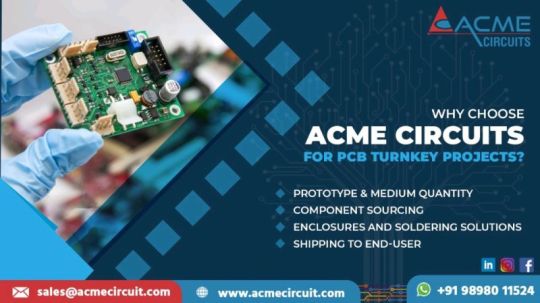
Visit for more information on PCB Manufacturers: https://www.acmecircuit.com/blog/
#PCBManufacturers#PCBManufacturing#PrintedCircuitBoard#CircuitBoardAssembly#CircuitBoardManufacturing#PCBBoardManufacturer#HighFrequencyPCB#PCBManufacturersNearMe#PCBManufacturer#PCBSupplier#PCBAssemblyServices#PCBAssemblyManufacturer#ElectronicCableAssembly#ElectronicContractServices#PCBExporters#PrintedCircuitBoardManufacturer#PCBManufacturingCompanies#PCBManufacturerIndia#PCBIndustry#PCBSolutions#ElectronicManufacturing#PCBPrototyping#PCBDesign#ElectronicsProduction#PCBQualityControl#ElectronicsEngineering#PCBTechnology#PCBExperts#PCBInnovation#PCBManufacturingProcess
0 notes
Text
Physical and Electrical Partitioning In PCB Design
Partitioning your design into physical and electrical sections can significantly reduce the number of through-holes you need in your PCB, thereby increasing production speed and cutting down on manufacturing costs. Here, we will explain what physical and electrical partitioning are how they are used in PC design, and how to create effective partitioning schemes in your PCB designs.
As you work on your next PCB design, you may be wondering how to implement physical and electrical partitioning in your design. These two factors are equally important to making the finished product successful, and both have a huge impact on the success of your design project as a whole. Stay with us if you’re looking to save time and money while producing high-quality products, read on!
Layout Considerations
When you’re laying out a Printed Circuit Board, you have two different considerations, such as physical, which is how your components are laid out on your printed circuit board; and electrical, which has to do with where you're going to put all of your wires. These two can be grouped when it comes time for assembly.
For example, if you plan to use surface-mount parts that require soldering instead of wire-wrapping, then you will want to make sure that there is enough space between these parts so that they can be easily soldered onto your PCB. If you don’t leave enough space between them, then there won’t be room for solder paste. The solder paste is a sticky substance used to hold down SMT parts during pcb assembly.
This makes soldering difficult or impossible and the same logic applies to wiring. If you don’t leave enough space between components, then your wires may not fit without being bent too much or getting in each other’s way. This can cause problems when it comes time to solder everything together, as well as with heat dissipation, and too many wires crammed into one area might block airflow and cause overheating issues.
On top of that, you also need to consider things like trace width and spacing. Trace width refers to how wide your traces are (the lines connecting individual pads on your PCB), while trace spacing refers to how far apart they are from each other. Trace width should always be smaller than trace spacing because having wider traces means more copper is needed per unit length which means higher cost and greater weight.
Traces are usually made using either a single solid line or multiple lines connected by vias. Single solid lines tend to be faster but less reliable than multiple lines connected by vias, but they’re also easier to design and cheaper. Vias are holes drilled through layers of material that allow traces on different layers to connect.However, vias increase complexity and cost. There are several tools available to help designers create their circuits. Some free software options include EagleCAD, Kicad, Altium Designer, and CAD. However, regardless of what software you choose to use, remember that layout is only half of the process.
Overlapping Impedance Nets & Ghost Nets
To create a circuit board with electrical & physical separation, you must insert impedance nets into your design. There are three different ways you can do that, including overlapping impedances, creating ghosts, or through a virtual ground plane. In some designs, more than one method is used. So, let’s see how and when to use them.
An overlapping impedance net has part of it on one side of a barrier, and part of it on another side. A ghost net is used when you have two nets that need to be separated but you don't want them physically separated because they are too close together or because they are too important for each other. A ghost net is just a virtual representation of an actual physical connection that exists between two parts of your circuit board.
A good example of why you might use a ghost PC board net instead of separating your nets with some physical method is if you have 2 power supplies that need to share ground. They can share ground by having their grounds tied together through some kind of wire.But, since they're both supplying power independently, we don't want them tied directly together at all times, but only when there is a current going through either one or both supplies. So what do we do? We create a ghost ground plane where we tie their grounds together. This way, when none ofthe supplies is active, there's no connection between them, and when either supply is active, there isa connection between them.
An electrical partitioning net does exactly what it sounds like. It partitions electrical signals from each other. In a design where you want to physically separate your nets, you can do that by creating an impedance plane that separates them. But, then how do you keep them electrically isolated? That's where a physical partitioning plane comes into play. This is just another name for a ghost ground plane, but instead of being used for sharing grounds between two supplies, it's used for keeping two parts of your circuit board electrically isolated from each other while still allowing communication between them.
One last thing about these three methods is thatyou can't use one without using at least one of the others. If you have a wall between two sections of your circuit board, there has to be some way for those sections to talk to each other. Otherwise, they wouldn't be able to pass power or data. So, if you have a wall, you need ghosts or an impedance plane on both sides of it. And if you have ghosts, there needs to be a wall somewhere too.
Why Would You Ever Choose One Method Over Another?
Well, overlapping impedances are good when you don't need high-frequency performance because they introduce more inductance than either of the other two methods. Ghosts are good when you don't care as much about electromagnetic interference or EMI because they don't create as much capacitance as either of the other two methods.
Whereas the physical partitioning nets are good when you want to keep your layout compact or if you have a design that's already laid out and you can't change it, as having a wall between two sections of your board is going to require some rework if it doesn't already exist.
So, you need to decide if you want your partitions at a high frequency or low frequency. For a high-frequency circuit board, you'll need to use overlapping impedances or ghosts; for a low-frequency circuit board, you can just go with physical partitioning nets.
Solving Unplanned Overlaps
It’s not uncommon for two different circuit boards or two different designs within a single board to overlap. Unplanned overlaps are hard to solve, but these tips will help you create better schematics so that you can avoid them.
Before you design your next PCB, make sure you follow all of these guidelines for PC Board Fabrication. By doing so, you’ll be able to identify overlaps before they occur and reduce your chances of creating any issues when manufacturing your product.
If you don’t have access to specialized tools or software, consider using some online tools like Google Sketch Up to help with your schematic design. These free programs allow you to build 3D models of your circuits, as well as export them into other applications like Eagle CAD or Altium Designer. This allows you to easily view how your components will fit together on a printed circuit board.
You should also use both software and hardware layout techniques to ensure that there aren’t any unplanned overlaps between your PCBs. While it may seem easier to just use one method, it’s important to understand how each technique works so that you can spot potential problems early on. For example, if you only use software-based layout techniques, then you might miss physical overlaps that would prevent a component from fitting onto your board.
Similarly, if you only rely on hardware-based methods, then you might overlook electrical conflicts that could lead to shorts or failures during testing. The best way to get around these kinds of issues is by using both types of layouts simultaneously. You can use a program like Altium Designer to lay out your circuit board, then print out an image of what you’ve created. Then take that printed image and place it over your actual PCB. This ensures that you catch any unplanned overlaps before they cause problems later on down the line.
Just remember, even though it takes more time upfront, double-checking everything twice is always worth it. With that said, there are still times when the overlap errors do slip through. When you find yourself in a situation where you need to resolve an issue like this, we recommend you double-check it. As it would become much easier to fix an error than it would be otherwise. You can also get professional help in this regard.
Would like to know more about physical and electrical partitioning in your designs or pcb assembly services? Write us at [email protected]
Website: https://pnconline.com/ Facebook: https://www.facebook.com/PNCONLINE Twitter: https://twitter.com/PNCINC Instagram: https://www.instagram.com/pnc_pcb/ Tumblr: https://www.tumblr.com/blog/view/pncinc Myspace :https://myspace.com/pncinc2020 Bresdel: https://bresdel.com/pncinc Call us: (973) 284-1600 Email us: [email protected] Location: PNC INC, 115 East Centre St.Nutley, NJ, 07110
0 notes
Link
Low pressure injection molding is a single-step process of filling the vacant cavities with molten polyamide or polyolefin materials. However, the process of low pressure injection molding requires a few preparatory measures. The experts at the company work closely with customers to understand their requirements before suggesting optimal injection over molding solutions.
0 notes