#Parallel SRAM
Explore tagged Tumblr posts
Visit Tumblr Blog
Explore Tumblr blogs with no restrictions, modern design and the best experience.
Last Seen Tumblr Blogs


Fun Fact
Post activity is at the highest at 4:00 pm EDT; notes peak at 10:00 pm EDT.
Text
https://www.futureelectronics.com/p/semiconductors--memory--RAM--static-ram--asynchronous/cy62167ev30ll-45zxit-infineon-9160615
EEPROMs chips, Non volatile RAM memory, NV RAM memories, ram memory
CY62167EV30 Series 16 Mb (1M x 16/2M x 8) 2.2 - 3.6 V 45 ns Static RAM -TSOP-48
#Infineon#CY62167EV30LL-45ZXIT#RAM#Static RAM#Asynchronous SRAM#EEPROMs chips#Non volatile RAM memory#NV RAM memories#ram memory#Static random access memory#Parallel SRAM#non volatile memories#non volatile SRAM types
1 note
·
View note
Text
https://www.futureelectronics.com/p/semiconductors--memory--RAM--nvram--quantum-trap-nvsram/m95m02-drmn6tp-stmicroelectronics-8011669
NV SRAM memory, nv ram, Parallel sram, non volatile memories, nonvolatile sram
M95M02 Series 2 Mb (256 K x 8) 5.5 V Serial SPI Bus EEPROM - SOIC-8
#STMicroelectronics#M95M02-DRMN6TP#RAM#NVRAM#Nonvolatile SRAM (NVSRAM)#Non volatile memory#static random access memory#NV SRAM memory#Parallel sram#nonvolatile sram#Types of Non Volatile SRAMs#Non volatile ram memory
1 note
·
View note
Text


11 MARS, 2016 ⊹ FREDAG, 18:58
20 APRIL, 2018 ⊹ VENDREDI, 20:26
28 DEZEMBER, 2018 ⊹ FREITAG, 19:30
15 MARZO, 2019 ⊹ VENERDÌ, 18:56
MARCH 29TH, 2019 ⊹ FRIDAY, 6:15PM
31 MAART, 2019 ⊹ ZONDAG, 20:13
28 APRIL, 2019 ⊹ ZONDAG, 21:39
02 SVIBANJ, 2025 ⊹ PETAK, 21:00
ALL NOORHELM VERSIONS + FIRST DATES
#Skam OG#Skam France#Druck#Skam Italia#Skam Austin#Skam NL#wtFOCK#Sram#Noorhelm#Marles#Winterberg#Incantava#Wilsen#Noliv#Zoenne#Klamaric#Skam OG 2x02#Skam France 2x02#Druck 2x02#Skam Italia 3x01#Skam Austin 2x02#Skam NL 2x03#wtFOCK 2x02#sorry Skam Esp didn't really do this season so I don't really feel like paralleling a non first date from Norandro here#Sram gave me so little to work with I'm so sorry
149 notes
·
View notes
Text


Utorak 7:49 + Details ✨
Ep2, Clip 2, "Good Down There"
#sram#sramcroatia#love the parallel with s1 clip 1#shows how Eva's grown since then#mysramdetailposts#mysrams2detailposts
12 notes
·
View notes
Text
https://www.futureelectronics.com/p/semiconductors--memory--RAM--static-ram--asynchronous/cy62167ev30ll-45zxi-infineon-9364399
Volatile memory, Computer memory, battery backed SRAM, ram memory
CY62167EV30 Series 16 Mb (1 M x 16/2 M x 8) 2.2 - 3.6 V 45 ns Static RAM-TSOP-48
#RAM#Static RAM#Asynchronous SRAM#CY62167EV30LL-45ZXI#Infineon#Volatile memory#Computer memory#battery backed SRAM#Random Access Memory#Static random access memory#Parallel SRAM memory#Nvram flash memory#what is Non Volatile SRAM
1 note
·
View note
Text
On Recovering From Disaster

Just before disaster struck with my 68030 homebrew, I had a plan to fork the project and take it in two directions in parallel.
The first would be my minimal Multibasic setup which was running great and was something I would be proud to exhibit at VCFSW '25.
Since that was working well, I didn't want to do anything that might make it not ready for the show. So I had assembled a second main board that I could use with other peripheral cards to continue development. My plan was to rework the memory map to move ROM and I/O addresses to the upper half of the 32-bit address space, which would allow me to use a DRAM card for up to 16MB of contiguous memory starting at address 0 — a perfect setup for running a proper OS
And then I burned up my good mainboard.
I had a spare CPLD on-hand, and I was able to get another 40MHz 68EC040 for cheap. But the 4Mbit SRAM chips are expensive, and I thought that if I was going to be paying for more SRAM, I should get the 12ns parts that would allow me to run RAM with no wait states at 50MHz. Which would require adapter boards, and more pin headers, and would have just driven the cost up even more.
Paralyzed by indecision and the rising cost, I decided to switch gears. I already have the DRAM board I built years ago, I just needed to get it working. And if I'm doing that, I may as well do the work on reorganizing my memory map.
So that's what I did. I made a new branch on my newly cleaned up repository, and set to work. I updated the mainboard bus controller logic to remove the no-longer-needed SRAM control, adjust the ROM address to start at 0x8000,0000, and move the 6850 UART address to 0x8008,0000. This freed up the entire 2GB space between 0x0000,0000 and 0x7FFF,FFFF for the DRAM card to use for main memory (my bus connector layout only allows for up to 16MB main memory, but that's plenty for my purpose).
Next, I needed to build the control logic for my DRAM board. I've done this once before on my Wrap030-ATX project a couple years ago, so I used that logic as a starting point. It … kind-of worked. Sometimes. Maybe.

I was getting random errors all over the place. Sometimes it was able to copy all of ROM into RAM and verify the copy without error, but it would fail when running code from RAM. Sometimes it wouldn't even pass the first two simple tests of writing a longword to RAM and reading it back.
Back to the data sheets to plan out the logic. I drew out a new timing diagram down to 1ns resolution, accounting for the specified propagation time for my CPLDs, and the measured signal delays for my CPU. This gave me the information I needed to build out a new state machine for the DRAM controller. In the process I also caught a few other bugs in my original logic, such as not ensuring the DRAM Write Enable strobe did not get asserted during refresh cycles.

The new state machine worked much better, but I got my timing off a bit. It worked reliably at 16MHz, but not at the intended 25MHz. At least it was working though; I can move forward with 16MHz.
The next thing to do was get my 8-port serial card working with this new setup. Every time the computer tried to access one of the 8 serial ports, it would get a bus error. This was a tough one that had me stuck for a while.
It looked like the serial card was getting addressed and asserting DSACK0# as expected, but I couldn't confirm the signal was making it back to the CPU. Every time I tried to measure the DSACK signals, the probes would increase the line capacitance (I think) too much and cause the whole computer to fail before it even got to the point of trying to address the serial ports.


I have the DSACK signals in a wired-or configuration. The logic on each card connects to the proper DSACK signal via an open-collector buffer, and is able to pull the signal low to signal that card acknowledging the bus cycle. The signal is then pulled back up to +5V by a 1kΩ resistor. This works well enough for small, slow systems, but with long bus wires or lots of chips on the bus, the extra capacitance means it can take a long time for that pull-up resistor to get the signal back up to +5V.
I made a change to my DRAM controller to actively drive the DSACK signals to +5V briefly at the end of a bus cycle before setting the pin to high-impedance. This helps ensure a fast rise time at the end of the cycle so it doesn't disrupt the next bus cycle.
It didn't fix the problem with the serial card, but it did allow me to actual probe the signals live to see what was happening — the Bus Error signal was getting asserted immediately after the CPU addressed the serial card. This didn't make much sense to me. My main board logic will assert Bus Error if no peripherals acknowledge a bus transaction within 64 clock cycles. Nothing should be asserting Bus Error so quickly.
Except … the main board bus controller. My original memory map used the lower half of the address space for the main board, and peripheral cards used the upper half. So my original main board logic was built to assert Bus Error immediately for an unused address in the lower half of the address space. I hadn't properly removed that bit of logic, so it was now asserting Bus Error for any accesses to the upper half of the address space that weren't used by the main board.
The challenges of working on a project after six years. I had forgotten that bit of logic was even there.
With that erroneous Bus Error assertation removed, the machine was finally able to properly load my Multibasic kernel and run BASIC for 8 users again.


At the moment it is running stable at 24MHz on my 25MHz-rated full 68030. It may not be the 50MHz high I was at, but after the frustration and disappointment of the past few weeks, I'm absolutely taking that as a win. 24MHz is incredible.
#mc68030#motorola 68k#motorola 68030#vcfsw#wrap030#retrotech#debugging#troubleshooting#homebrew computing#homebrew computer#retro computing
23 notes
·
View notes
Text
parallels in sram episode 2 clip 1 and the sram teaser trailer


46 notes
·
View notes
Text
✨SRAM Parallels✨


Two very different moments in time and two very different conversations. I just think it’s interesting though how the mention of Roko is used to introduce much needed significant conversations that both have such a deep impact.
9 notes
·
View notes
Text
0 notes
Text

Best VLSI Projects for Final Year Students
Here are some great VLSI project ideas for final-year students:
1. Image Processing System on FPGA: Algorithm, such as edge detection or image filtering should be performed through the usage of FPGAs for optimal performance.
2. Low-Power SRAM Design: Design and simulate a low-power Static Random Access Memory (SRAM) cell, targetting leakage and dynamic power dissipation.
3. Digital Signal Processor (DSP) Design: Design an example of a DSP that will allow a specific signal to be filtered or, for instance, undergo FFT.
4. Wireless Sensor Network (WSN) Protocol Implementation: Devise a VLSI based sensor node for wireless communication that will support protocols used in data transmission.
5. Reconfigurable Hardware Architecture: It is necessary to elaborate a box which is able to evolve in order to support several applications: in this context, it is possible to try to reconfigure parts of the hardware during the runtime according to the specific needs of the client application.
6. Cryptographic Hardware Accelerator: Propose and design a device for which you could use cryptographic algorithms or primitives including AES or RSA where optimization of both speed optimization and security is important.
7. System-on-Chip (SoC) Design: Selected h/w architects use Verilog or VHDL to design a including microcontroller, memory and other peripherals.
8. Artificial Neural Network (ANN) on FPGA: Devise a mini ANN for image recognition and other related work and optimally use the features of parallel processing provisioned by FPGAs.9. Automated VLSI Testing Tool: Design a testing and validation software system that has reduced time and eliminated errors in conducting tests of VLSI designs (Very Large Scale Integration).
10. Temperature Sensor with Data Logger: It will be a VLSI (Very Large Scale Integration) chip for measuring temperature and recording data, with the capability to display the data on a PC or a mobile connection.
All these project proposals present prospects to learn diverse aspects of VLSI design and implementation in addition to enhancing creativity. Choose one that you are interested in and which you can afford to do!
#vlsi#finalyear#verylargescaleintegration#VLSIDesign#engineeringstudents#studentsprojects#takeoffedugroup#takeoffprojects
0 notes
Text


12 NOVEMBER, 2015 ✦ TORSDAG, 13:20
13 MARS, 2018 ✧ MARDI, 09:00
10 MAGGIO, 2018 ✦ GIOVEDÌ, 14:40
16 MAI, 2018 ✧ MITTWOCH, 11:29
01 JUNE, 2018 ✦ THURSDAY, 3:34PM
25 OKTOBER, 2018 ✧ DONDERDAG, 12:34
27 OCTUBRE, 2018 ✦ SÁBADO, 21:17
16 NOVEMBER, 2018 ✧ VRIJDAG, 10:11
04 PROSINAC, 2024 ✦ SRIJEDA, 15:56
#Skam#SkamEdit#Skam OG#Skam France#Druck#Skam Italia#Skam Austin#Skam España#Skam NL#wtFOCK#Sram#Noora Amalie Sætre#Manon Demissy#Mia Amalie Winter#Eleonora Francesca Sava#Grace Olsen#Liv Reijners#Nora Grace#Zoë Loockx#Nora Klarić Šelem#Parallels#Skam Remakes#Skamverse Daily#1x06#1x07#s1#I've chosen to show what they said after the 'whatever it is'/whatever they've said instead/after the cliché part#how many times have I giffed Zoë saying 'fcking living cliché'? Never enough tho :)#also Grace's 'move' still means so much to me <3
307 notes
·
View notes
Text
https://www.futureelectronics.com/p/semiconductors--memory--RAM--static-ram--asynchronous/cy62167ev30ll-45bvit-infineon-7951205
Memory ICs, Parallel SRAM memory, Static random access memory, circuits, chips
CY62167EV30 Series 16 Mb (1M x 16/2M x 8) 2.2 - 3.6 V 45 ns Static RAM -TSOP-48
#Infineon#CY62167EV30LL-45BVIT#RAM#Static RAM#Asynchronous SRAM#Static random access memory#circuits#chips#Nonvolatile sram#SRAM#EPROMs#EEPROMs#Digital to analog converter#Sram memory card#sram memory chips#sram memory
1 note
·
View note
Text
Gaudi 2 Intel Benchmarks GenAI Performance Against NV H100

Gaudi 2 Intel
For GenAI Performance, Intel Gaudi 2 is Still the Only Benchmarked Option Besides NV H100. The results of the industry-standard MLPerf v4.0 benchmark for inference were released by MLCommons. The company’s dedication to bringing “AI Everywhere” with a wide range of competitive solutions is reinforced by Intel’s results for its Intel Gaudi 2 accelerators and 5th Gen Intel Xeon Scalable CPUs with Intel Advanced Matrix Extensions (Intel AMX).
When it comes to generative AI (GenAI) performance, the Gaudi 2 Intel AI accelerator is still the sole benchmarked substitute for the Nvidia H100, offering excellent value for the money. Moreover, Intel continues to be the only manufacturer of server CPUs to provide MLPerf findings.
According to MLPerf Inference v3.1, the average improvement in Intel’s 5th Gen Xeon results over 4th Gen Intel Xeon processors was 1.42x. The Reason It Matters Intel’s MLPerf findings provide clients industry-standard standards to assess AI performance, building on its training and inference performance from prior MLPerf rounds.
Intel Gaudi 2 vs Nvidia NV H100 High-Performance AI Accelerator: This robust GPU is intended for usage in data centres for applications such as real-time deep learning inference, rapid data analytics, high-performance computing (HPC), and data analysis. Leading Performance: The H100 offers up to 7x better performance for HPC workloads than prior versions. LLM, or large language model Amicable: With its specialised Transformer Engine, which is intended to handle large LLMs, conversational AI activities may be performed up to 30 times quicker. Scalability and Security: To handle exascale workloads, the NVIDIA NVLink Switch System connects up to 256 H100 GPUs, and NVIDIA Confidential Computing, a built-in feature, secures data and applications. Intel Gaudi 2 The popular large language models (LLMs) and multimodal models that are covered by the Intel Gaudi software package are still growing. Intel submitted the Gaudi 2 accelerator results for the state-of-the-art models Llama v2-70B and Stable Diffusion XL for MLPerf Inference v4.0.
Hugging Face Text Generation Inference (TGI) has been quite popular, and Gaudi’s Llama work took use of this by using the TGI toolbox, which allows for tensor parallelism and continuous batching, thereby improving the efficiency of real-world LLM scaling. Gaudi 2 yielded 8035.0 and 6287.5 tokens-per-second for offline and server tokens, respectively, for Llama v2-70B. Gaudi 2 yielded 6.26 and 6.25 offline samples per second and server queries per second on Stable Diffusion XL, respectively.
Intel Gaudi 2 specs 7nm process technology Dual matrix multiplication engines (MME) and 24 programmable tensor processor cores (TPC) make up the heterogeneous compute architecture. Memory: 48 MB of SRAM and 96 GB of HBM2E onboard memory Networking: 24 on-chip integrated 100 Gbps Ethernet ports The Gaudi 2 Intel delivers outstanding speed and scalability and is optimised for deep learning training and inference applications. It has a heterogeneous computational architecture with twin matrix multiplication engines and 24 programmable tensor processor cores, and it is based on a 7nm manufacturing technology. The Gaudi 2 can effectively perform a range of deep learning tasks because to its design.
Additionally, the Gaudi 2 Intel has 96GB of HBM2E memory built-in, offering enough of capacity for data access. Moreover, the Gaudi 2 has 24 on-chip 100 Gbps Ethernet connectors, allowing several Gaudi 2 Intel accelerators to communicate at high speeds. Because of this, the Gaudi 2 is a good fit for deep learning clusters of any size.
Intel Gaudi 2 price These findings indicate that the Intel Gaudi 2 is still a competitive price. AI Will Be Everywhere in Intel Vision 2024
They are pleased to announce Intel Vision, which will be held in Phoenix, Arizona, on April 8–9, 2024. their flagship event, Intel Vision, brings together elite leaders in business and technology to discuss the most recent developments in the industry and solutions related to client, edge, data Centre, and cloud innovations.
Sign up now to take part in thought-provoking roundtables, captivating demonstrations, and cutting-edge AI insights with Intel executives and distinguished guests that will help you realise your technological vision.e/performance, a crucial factor to take into account when examining the total cost of ownership (TCO).
Concerning the Intel 5th Generation Xeon Outcomes: With advancements in both hardware and software, Intel’s 5th generation Xeon processors outperformed 4th generation Intel Xeon processors in MLPerf Inference v3.1, with a geomean increase of 1.42x. For instance, the 5th Gen Xeon entry demonstrated around 1.8x performance increases over the v3.1 submission for GPT-J with software optimisations including continuous batching. In a similar vein, MergedEmbeddingBag and further Intel AMX optimisations allowed DLRMv2 to provide around 1.8x speed increases with 99.9 accuracy.
Intel takes great pride in working together with OEM partners, like Quanta, Supermicro, Cisco, Dell, and WiWynn, to enable them to submit their own MLPerf results. Additionally, beginning in 2020, Intel has provided MLPerf results for four generations of Xeon CPUs; in many of these submissions, Xeon serves as the host CPU.
How to Utilise Intel Developer Cloud AI Solutions: The Intel Developer Cloud offers evaluations of 5th generation Xeon CPUs and Intel Gaudi 2 accelerators. Users may manage AI computing resources, execute training and inference production workloads at scale (LLM or GenAI), and do much more in this environment.
What to Watch For: Stay tuned for an update on Intel Gaudi 3 AI accelerators and additional information about Intel’s plan to deliver “AI Everywhere” at Intel Vision 2024.
Read more on Govindhtech.com
#intel#nvh100#intelgaudi2#genai#ai#cpu#stablediffusion#llm#intelvision#technology#technews#govindhtech
0 notes
Text
Mikrocontroller ESP32C3 von Seeed Studio
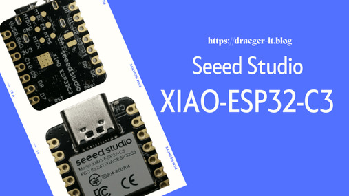
In diesem Beitrag möchte ich dir den Mikrocontroller ESP32C3 von der Firma Seeed Studio vorstellen.

Dieser Mikrocontroller trägt durch seine geringen Abmaße mal wirklich zurecht die Bezeichnung "Mikrocontroller".

ESP32-C3 von Seeed Studio

ESP32-C3 von Seeed Studio (Rückseite) Von der Firma Seeed Studio habe ich dir bereits den Seeed Studio XIAO RP2040 – ein Zwerg mit großer Leistung vorgestellt, welcher die gleichen Abmaße hat, wie der hier gezeigte ESP32C3.

Vergleich XIAO RP2040 mit ESP32-C3 von Seeed Studio
Bezug des ESP32C3 von Seeed Studio
Den mir vorliegenden Mikrocontroller habe ich auf berrybase.de für 8,45 € zzgl. Versandkosten erstanden. ShopPreisVersandkostenhttps://www.berrybase.de8,45 €3,95 €https://botland.de7,90 €4,95 €https://eckstein-shop.de7,95 €1,99 € Lieferumfang Der Mikrocontroller wird zusammen mit einer externen Antenne in einer kleinen Plastiktüte geliefert.

Mikrocontroller ESP32-C3 verpackt

ESP32-C3 von Seeed Studio mit externer Antenne Damit du diesen also auf ein Breadboard stecken möchtest, benötigst somit noch zusätzlich zwei 7-Pin Stiftleisten im 2,54 mm Rasterformat. Diese Stiftleisten bekommst du auf ebay.de bereits ab knapp 3 € für ein ganzes Pack mit 5 Leisten mit je 20 Pins.
Technische Daten des ESP32C3
Nachfolgend zunächst die technischen Daten des ESP32C3. ProzessorESP32-C3, 32bit, RISC-VTaktgeschwindigkeit160 MHzSpeicher400 KB SRAM, 4 MB FlashSchnittstellenI²C, UART, SPI, I²Sdrahtlose SchnittstellenWiFi, Bluetooth Low Energy 5 (BLE)Pins11 digitale PWM Pins, 4 analoge PinsFeaturesReset-Button, Boot-Button, Lötaugen für JTAG & Batterie Einen Vergleich mit den anderen Mikrocontrollern sowie weitere Informationen findest du auf der englischen Seite Getting Started with Seeed Studio XIAO ESP32C3.
Pinout des ESP32C3
Der Mikrocontroller hat nachfolgendes Pinout.

Pinout des Mikrocontrollers ESP32-C3
Stiftleisten anlöten
Wie erwähnt liegen dem Mikrocontroller keine Stiftleisten bei, jedoch werden diese benötigt um diesen mit Sensoren & Aktoren per Breadboardkabel oder einem XIAO Grove Base zu verbinden. Ich empfehle dir den Mikrocontroller auf ein Breadboard zu stecken, denn so kannst du die Stiftleisten in einem vernünftigen 90° Winkel anlöten.


XIAO Grove Base Shield
Wenn wir die Stiftleisten angelötet haben, dann können wir den Mikrocontroller auf das XIAO Grove Base Shield stecken und haben somit nicht nur die Möglichkeit Sensoren/Aktoren per Breadboardkabel zu verbinden, sondern auch per Grove Adapter.


Auch hier habe ich noch zusätzlich die Stiftleisten angelötet und kann somit parallel Breadboardkabel und Grove Adapter anschließen.
Einrichten und Programmieren des ESP32-C3 in der Arduino IDE 2.0
Im nachfolgenden YouTube-Video erläutere ich dir, wie du den Mikrocontroller in der Arduino IDE 2.0 einrichtest und ein erstes kleines Programm schreibst. https://youtu.be/yu5lj6qLxVk
Programmieren in der Arduino IDE
Gem. Hersteller Seeed Studio kann dieser Mikrocontroller in der Arduino IDE programmiert werden. Dazu musst du jedoch zunächst den Boardtreiber installieren. Zunächst musst du jedoch die Adresse zu dem benötigten Boardtreiber in den Einstellungen der Arduino IDE hinzufügen. https://raw.githubusercontent.com/espressif/arduino-esp32/gh-pages/package_esp32_index.json Der Mikrocontroller wird unter Tools > Port als "Adafruit QT Py ESP32-C3" erkannt.

Wenn wir den Port gewählt haben, wählen wir noch aus der Liste der Mikrocontroller von Tools > Board: xyz > esp32 > XIAO_ESP32C3 aus.

LED blinken am ESP32-C3 von Seeed Studio
Zunächst ein kleines Beispiel mit einer LED am ESP32.

Mikrocontroller ESP32-C3 mit Grove LED Hier nun der Code um eine LED welche am GPIO8 angeschlossen ist im Intervall von 250 Millisekunden blinken zu lassen. //LED am GPIO8 angeschlossen #define led 8 void setup() { //definieren das der Pin //der LED als Ausgang dient pinMode(led, OUTPUT); } void loop() { //aktivieren der LED digitalWrite(led, HIGH); //eine kleine Pause von 250 ms. delay(250); //deaktivieren der LED digitalWrite(led, LOW); //eine kleine Pause von 250 ms. delay(250); } Read the full article
1 note
·
View note
Text
Steven Rindner on Gravel Biking: Tools and Accessories
Steven Rindner on Gravel Biking: What do You Need?
Over the past few years, we've witnessed a huge increase in the number of bikes and accessories on offer, in parallel with the growing popularity of gravel biking.
SRAM, Shimano, and Campagnolo have all launched gravel groupsets designed with a better gear range than typical cycling groupsets, which have become commonplace on gravel bike setups, as bikers like Steven Rindner note.
The number of electric gravel bikes is also increasing, allowing more riders to explore steeper and further than ever before.
Flared handlebars are now quite common for gravel bikes, giving more stability on the drops, and many riders opt for wider bars than you'd typically find on standard road bikes.
Several technologies are also coming across, from the world of mountain biking to gravel riding.

The integration of suspension into seat posts and stems aims to relieve discomfort caused by rough terrain. In addition, gravel bike suspension is now available in the form of the Lauf Grit fork (30mm travel), Niner's MCR 9 RDO full suspension gravel bike (50mm travel), and the RockShox Rudy Ultimate XPLR fork (30 or 40mm travel).
Tubeless tire inserts, lightweight foam tubes that reduce your puncture risk, and gravel bike dropper posts, which lower the seat post and alter your body weight on the bike on steep descents, also have MTB origins.
What tools do you need to take for gravel riding?
As bikers like Steven Rindner note, you have to ensure you carry all the necessary spares and tools, including a quick link and chain tool, tire boot, tubeless repair kit, spare tubes, and a high-volume pump. If you're heading out into the wild, bringing cable ties, a spare derailleur hanger, tape, and even brake pads is a great idea.

Planning before you ride, with your route loaded on your phone, GPS bike computer, or smartwatch, can be invaluable. Cycling apps, such as Komoot, are also very helpful.
In case of battery failure, Steven Rindner and other biking enthusiasts point out that people shouldn't forget a paper map on trips into the wilderness. In this environment, you should pack water and plenty of snacks for your ride. There's nothing worse than biking in the middle of nowhere without a resupply point for miles.
Read more about the benefits of thru-hiking, bikepacking, performance cycling, and gravel biking by subscribing to this Steven Rindner page.
1 note
·
View note
Text
NXP and Xiaomi Vela jointly build an IoT ecosystem to provide a powerful technology engine for the IoT development community
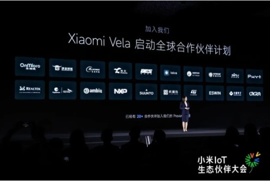
【Lansheng Technology News】Recently, at the 2023 Xiaomi IoT Ecological Partner Conference, NXP Semiconductors was invited to attend as an important partner of Xiaomi and demonstrated the powerful technical resource support provided to the Xiaomi Vela ecological community.
Xiaomi Vela is an embedded IoT software platform built on the open source real-time operating system NuttX and customized for consumer-grade IoT. It can provide a unified software platform on various IoT hardware, shielding the differences in underlying hardware. Through rich components and standardized software frameworks, it provides a unified software interface for upper-level device developers to open up fragmented things. Networked application scenarios greatly reduce the complexity of development and improve development efficiency.
As a global ecological partner of Xiaomi Vela, NXP is deeply involved in the construction of the ecosystem of this development community and has launched a series of technical resources. At this event, NXP highlighted the i.MX RT1060 EVK development kit.
NXP's i.MX RT1060 cross-border MCU is based on the 600MHz Arm Cortex-M7 core and has 1MB on-chip SRAM. It has strong real-time performance and high integration, and is suitable for various industrial and IoT applications. The i.MX RT1060 series provides 2D graphics, camera and various memory interfaces, as well as a wide range of connection interfaces, including UART, SPI, I2C, USB, 2 10/100M Ethernet interfaces and 3 CAN interfaces. Its other features for real-time applications include: high-speed GPIO, CAN-FD, and synchronous parallel NAND/NOR/PSRAM controller.
In addition, i.MX RT1060 has a 2D hardware graphics acceleration PXP module, 3 I2S interfaces for high-performance multi-channel audio, and supports LCD display controller (up to WXGA 1366 x 768). The i.MX RT1060 is available in 225BGA and 196BGA packages, providing greater flexibility with an extended temperature range of -40°C to 125°C.
The i.MX RT1060 series can be developed using NXP's official MCUXpresso tool chain, including SDK, IDE options, and security configuration and configuration tools, enabling rapid development and supporting various real-time operating systems (RTOS) such as FreeRTOS, Xiaomi Vela, Nuttx, Zephyr, etc. .
Xiaomi Vela is fully scalable from micro (8-bit) to mid-range embedded (64-bit) systems with a high degree of standards compliance, easy to port, fully open, highly real-time and powerful. i.MX RT1060 fully supports Xiaomi Vela. Currently supported drivers include ADC, CAN, eLCDIF, ENC, ENET, GPIO, I2S, PWM, SPI, UART and USB. It also supports Vela’s LVGL Demo and can be adapted to Xiaomi The upper component of Vela framework. This combination of soft and hard will provide a powerful technical engine for the development of the Xiaomi Vela ecological community.
Lansheng Technology Limited, which is a spot stock distributor of many well-known brands, we have price advantage of the first-hand spot channel, and have technical supports.
Our main brands: STMicroelectronics, Toshiba, Microchip, Vishay, Marvell, ON Semiconductor, AOS, DIODES, Murata, Samsung, Hyundai/Hynix, Xilinx, Micron, Infinone, Texas Instruments, ADI, Maxim Integrated, NXP, etc
To learn more about our products, services, and capabilities, please visit our website at http://www.lanshengic.com
0 notes