#VHDL Architecture
Explore tagged Tumblr posts
Visit Tumblr Blog
Explore Tumblr blogs with no restrictions, modern design and the best experience.
Last Seen Tumblr Blogs


Fun Fact
The KCSC sent more than 20K requests to delete posts related to prostitution and porn to Tumblr from January to June 2017.
Text
youtube
VHDL Tutorial : Your First VHDL Design: VHDL Entity & Architecture - A Beginner's Guide
Welcome to the ultimate beginner's guide for Your First VHDL Design! In this video, we will dive into the fundamentals of VHDL Entity and Architecture and provide you with a comprehensive understanding of the topic. Whether you are new to VHDL or looking to refresh your knowledge, this guide is designed to help you get started and pave your way to becoming an expert VHDL designer. In this tutorial, we will cover the basics of VHDL, starting with the VHDL Entity and its crucial role in the design process. You will learn how to define and describe the inputs and outputs of your VHDL design using the Entity section, providing the necessary specifications for your project. Moving on, we will explore the VHDL Architecture, which defines the actual implementation of your design. Through a step-by-step walkthrough, you will discover how to construct the architecture block by block, ensuring a well-structured and functional VHDL design. To make the learning experience more practical, we will dive into real-world examples and demonstrate each concept using a popular VHDL software tool. You'll witness the transition from theory to practice, gaining hands-on experience in VHDL design. With this beginner's guide, you'll not only grasp the essentials of VHDL Entity and Architecture but also acquire the ability to kickstart your own VHDL designs, opening up a wide range of possibilities in digital circuit design. Subscribe to our channel for more exciting VHDL tutorials and stay tuned for upcoming videos in this series where we will explore advanced VHDL concepts and applications.
Subscribe to "Learn And Grow Community"
YouTube : https://www.youtube.com/@LearnAndGrowCommunity
LinkedIn Group : https://www.linkedin.com/groups/7478922/
Blog : https://LearnAndGrowCommunity.blogspot.com/
Facebook : https://www.facebook.com/JoinLearnAndGrowCommunity/
Twitter Handle : https://twitter.com/LNG_Community
DailyMotion : https://www.dailymotion.com/LearnAndGrowCommunity
Instagram Handle : https://www.instagram.com/LearnAndGrowCommunity/
Follow #LearnAndGrowCommunity
#VHDL#VHDL Entity#VHDL Architecture#VHDL Design#Beginner's Guide#Digital Circuit Design#VHDL Tutorial#VHDL Basics#VHDL Examples#VHDL Software#Learn VHDL#VHDL Learning#VHDL Step-by-step#VHDL Introduction#VHDL Fundamentals#VHDL Engineering#Hardware Design#Circuit Design#Xilinx ISE#Xilinx Vivado#Digital#ASIC#Engineering#Students#Training#Tutorial#Altera#Hardware description language#modeling style#data flow
1 note
·
View note
Text
Understanding FPGA Architecture: Key Insights
Introduction to FPGA Architecture
Imagine having a circuit board that you could rewire and reconfigure as many times as you want. This adaptability is exactly what FPGAs offer. The world of electronics often seems complex and intimidating, but understanding FPGA architecture is simpler than you think. Let’s break it down step by step, making it easy for anyone to grasp the key concepts.
What Is an FPGA?
An FPGA, or Field Programmable Gate Array, is a type of integrated circuit that allows users to configure its hardware after manufacturing. Unlike traditional microcontrollers or processors that have fixed functionalities, FPGAs are highly flexible. You can think of them as a blank canvas for electrical circuits, ready to be customized according to your specific needs.
How FPGAs Are Different from CPUs and GPUs
You might wonder how FPGAs compare to CPUs or GPUs, which are more common in everyday devices like computers and gaming consoles. While CPUs are designed to handle general-purpose tasks and GPUs excel at parallel processing, FPGAs stand out because of their configurability. They don’t run pre-defined instructions like CPUs; instead, you configure the hardware directly to perform tasks efficiently.
Basic Building Blocks of an FPGA
To understand how an FPGA works, it’s important to know its basic components. FPGAs are made up of:
Programmable Logic Blocks (PLBs): These are the “brains” of the FPGA, where the logic functions are implemented.
Interconnects: These are the wires that connect the logic blocks.
Input/Output (I/O) blocks: These allow the FPGA to communicate with external devices.
These elements work together to create a flexible platform that can be customized for various applications.
Understanding Programmable Logic Blocks (PLBs)
The heart of an FPGA lies in its programmable logic blocks. These blocks contain the resources needed to implement logic functions, which are essentially the basic operations of any electronic circuit. In an FPGA, PLBs are programmed using hardware description languages (HDLs) like VHDL or Verilog, enabling users to specify how the FPGA should behave for their particular application.
What are Look-Up Tables (LUTs)?
Look-Up Tables (LUTs) are a critical component of the PLBs. Think of them as small memory units that can store predefined outputs for different input combinations. LUTs enable FPGAs to quickly execute logic operations by “looking up” the result of a computation rather than calculating it in real-time. This speeds up performance, making FPGAs efficient at performing complex tasks.
The Role of Flip-Flops in FPGA Architecture
Flip-flops are another essential building block within FPGAs. They are used for storing individual bits of data, which is crucial in sequential logic circuits. By storing and holding values, flip-flops help the FPGA maintain states and execute tasks in a particular order.
Routing and Interconnects: The Backbone of FPGAs
Routing and interconnects within an FPGA are akin to the nervous system in a human body, transmitting signals between different logic blocks. Without this network of connections, the logic blocks would be isolated and unable to communicate, making the FPGA useless. Routing ensures that signals flow correctly from one part of the FPGA to another, enabling the chip to perform coordinated functions.
Why are FPGAs So Versatile?
One of the standout features of FPGAs is their versatility. Whether you're building a 5G communication system, an advanced AI model, or a simple motor controller, an FPGA can be tailored to meet the exact requirements of your application. This versatility stems from the fact that FPGAs can be reprogrammed even after they are deployed, unlike traditional chips that are designed for one specific task.
FPGA Configuration: How Does It Work?
FPGAs are configured through a process called “programming” or “configuration.” This is typically done using a hardware description language like Verilog or VHDL, which allows engineers to specify the desired behavior of the FPGA. Once programmed, the FPGA configures its internal circuitry to match the logic defined in the code, essentially creating a custom-built processor for that particular application.
Real-World Applications of FPGAs
FPGAs are used in a wide range of industries, including:
Telecommunications: FPGAs play a crucial role in 5G networks, enabling fast data processing and efficient signal transmission.
Automotive: In modern vehicles, FPGAs are used for advanced driver assistance systems (ADAS), real-time image processing, and autonomous driving technologies.
Consumer Electronics: From smart TVs to gaming consoles, FPGAs are used to optimize performance in various devices.
Healthcare: Medical devices, such as MRI machines, use FPGAs for real-time image processing and data analysis.
FPGAs vs. ASICs: What’s the Difference?
FPGAs and ASICs (Application-Specific Integrated Circuits) are often compared because they both offer customizable hardware solutions. The key difference is that ASICs are custom-built for a specific task and cannot be reprogrammed after they are manufactured. FPGAs, on the other hand, offer the flexibility of being reconfigurable, making them a more versatile option for many applications.
Benefits of Using FPGAs
There are several benefits to using FPGAs, including:
Flexibility: FPGAs can be reprogrammed even after deployment, making them ideal for applications that may evolve over time.
Parallel Processing: FPGAs excel at performing multiple tasks simultaneously, making them faster for certain operations than CPUs or GPUs.
Customization: FPGAs allow for highly customized solutions, tailored to the specific needs of a project.
Challenges in FPGA Design
While FPGAs offer many advantages, they also come with some challenges:
Complexity: Designing an FPGA requires specialized knowledge of hardware description languages and digital logic.
Cost: FPGAs can be more expensive than traditional microprocessors, especially for small-scale applications.
Power Consumption: FPGAs can consume more power compared to ASICs, especially in high-performance applications.
Conclusion
Understanding FPGA architecture is crucial for anyone interested in modern electronics. These devices provide unmatched flexibility and performance in a variety of industries, from telecommunications to healthcare. Whether you're a tech enthusiast or someone looking to learn more about cutting-edge technology, FPGAs offer a fascinating glimpse into the future of computing.
2 notes
·
View notes
Text
The Growing Demand for VLSI Training and Career Opportunities
The Importance of VLSI in the Semiconductor Industry
The field of Very Large Scale Integration (VLSI) has seen exponential growth in recent years, driven by the rapid advancements in semiconductor technology. With the ever-increasing demand for high-performance chips used in smartphones, computers, automotive electronics, and artificial intelligence, VLSI has become a crucial aspect of modern electronics. The need for skilled professionals in this domain is rising, leading to the emergence of specialized training institutes that equip students with the necessary knowledge and hands-on experience. Engineers with expertise in VLSI design and verification are highly sought after by global technology firms, making this an attractive career path for aspiring electronics engineers.
Skills and Knowledge Required for a Career in VLSI
A successful career in VLSI requires a deep understanding of digital design, analog and mixed-signal design, system-on-chip (SoC) architecture, and verification methodologies. Programming skills in hardware description languages like VHDL and Verilog are essential, along with expertise in Electronic Design Automation (EDA) tools. The learning curve for VLSI professionals is steep, as it involves both theoretical concepts and practical applications. Many engineers and students opt for professional training programs to bridge the gap between academic knowledge and industry expectations. In particular, enrolling in one of the top 10 VLSI training institutes can provide a strong foundation and industry exposure, helping individuals stay ahead in this competitive field.
The Role of Training Institutes in Shaping VLSI Professionals
VLSI training institutes play a significant role in preparing students for real-world industry challenges. These institutes offer comprehensive courses covering fundamental to advanced topics, ensuring that learners gain practical expertise. Training programs often include hands-on projects, industry-relevant case studies, and internship opportunities that enhance problem-solving abilities. Many training centers collaborate with semiconductor companies, providing students with valuable networking opportunities and job placements. Among the many options available, VLSI institutes in Bangalore are particularly renowned for their high-quality education and strong industry connections. As Bangalore is a hub for semiconductor companies, students trained here have a higher chance of securing rewarding job opportunities.
Career Opportunities and Future Scope in VLSI
With the rapid expansion of the semiconductor industry, the demand for skilled VLSI engineers continues to grow. Companies specializing in chip design, manufacturing, and embedded systems actively seek trained professionals who can contribute to the development of cutting-edge technologies. Career opportunities in this field are diverse, ranging from digital and analog design to verification and testing. Additionally, with the emergence of AI, IoT, and 5G, the scope for VLSI professionals is expanding further. Salaries in this domain are highly competitive, and individuals with specialized training can secure lucrative positions in leading global technology firms. Those who continue upgrading their skills and staying updated with industry trends will find themselves at the forefront of technological advancements.
Choosing the Right VLSI Training Institute
Selecting the right training institute is a crucial step in building a successful career in VLSI. Factors such as faculty expertise, course curriculum, industry collaborations, hands-on training, and placement assistance should be carefully evaluated before making a decision. Institutes that offer mentorship, real-time project exposure, and certification programs can significantly enhance a student’s career prospects. One such institute that has gained recognition for providing quality VLSI training is Takshila VLSI.com. By enrolling in a reputed training institute, aspiring VLSI professionals can equip themselves with the necessary skills and knowledge to excel in the semiconductor industry.
0 notes
Text
Master ASIC Design and Verification Training Today

In today’s fast-paced semiconductor industry, mastering ASIC (Application-Specific Integrated Circuit) design and verification is essential for engineers and professionals looking to advance their careers. With cutting-edge technology and increasing demand for customized chip designs, the need for skilled ASIC designers is greater than ever. If you are eager to enhance your expertise, ASIC Design and Verification Training is the perfect opportunity to gain in-depth knowledge and practical skills.
Why Choose ASIC Design and Verification Training?
ASIC design is a complex yet rewarding field that requires a deep understanding of digital circuits, system architecture, and verification methodologies. This training equips you with:
Fundamental and Advanced ASIC Design Concepts – Learn the principles of ASIC development, from design to implementation.
Verification Techniques – Master simulation-based verification, formal verification, and functional testing.
Industry-Standard Tools – Get hands-on experience with tools like Verilog, VHDL, SystemVerilog, and UVM.
Practical Projects and Case Studies – Work on real-world projects to strengthen your problem-solving abilities.
Expert Guidance – Learn from industry professionals with years of experience in ASIC design and verification.
Who Should Enroll?
This training is ideal for:
Engineering students and graduates looking to specialize in VLSI and ASIC design.
Working professionals aiming to upskill in semiconductor design.
Anyone passionate about learning digital design and verification methodologies.
Career Benefits of ASIC Design and Verification Online Training
With expertise in ASIC design and verification, you can unlock various career opportunities in semiconductor and electronics industries. Job roles include:
ASIC Design Engineer
Verification Engineer
FPGA Engineer
VLSI Design Engineer
Embedded Systems Engineer
Enroll Today and Advance Your Career!
Don’t miss the chance to boost your career in the high-demand field of ASIC design. Join ASIC Design and Verification Training today and gain the skills needed to thrive in the semiconductor industry. Start your journey towards success with expert-led training and hands-on experience.
At Multisoft Virtual Academy, we provide comprehensive training programs to help tech enthusiasts achieve professional excellence. Sign up now and take the next step in your career!
0 notes
Text
ASIC Design of Complex Multiplier: A Comprehensive Overview
In the modern era of digital signal processing (DSP) and communication systems, multipliers play a pivotal role. Complex multipliers, in particular, are essential in a wide array of applications such as Fast Fourier Transforms (FFT), Digital Down Converters (DDC), and MIMO communication systems. The design of an Application-Specific Integrated Circuit (ASIC) for a complex multiplier presents unique challenges and opportunities. In this blog, we delve into the intricacies of ASIC design for complex multipliers, exploring their architecture, design methodologies, and optimization techniques.
What is a Complex Multiplier?
A complex multiplier is a circuit that performs multiplication of two complex numbers. Mathematically, if and are two complex numbers, their product is given by:
This equation shows that a complex multiplier requires four real multiplications and two real additions/subtractions.
Key Considerations in ASIC Design of Complex Multipliers
Area Efficiency: ASIC designs often operate under strict area constraints. Optimizing the layout and minimizing the number of logic gates are crucial for reducing silicon area.
Power Consumption: Power efficiency is paramount, especially for portable or battery-operated devices. Techniques like clock gating, operand isolation, and optimized arithmetic circuits help in reducing dynamic and static power consumption.
Speed: High-speed operation is critical for real-time applications. The multiplier design must ensure minimal propagation delay while maintaining accuracy.
Precision: Depending on the application, the design may require fixed-point or floating-point arithmetic, which significantly impacts complexity and performance.
Process Technology: The choice of CMOS technology node (e.g., 28nm, 14nm, etc.) influences performance, power, and area (PPA) trade-offs.
Architecture of a Complex Multiplier
A typical complex multiplier architecture consists of the following components:
Four Real Multipliers: These are the core computation units.
Two Adders/Subtractors: These units perform the addition and subtraction of intermediate results.
Pipeline Registers (Optional): Pipelining enhances throughput by reducing the critical path.
To optimize the design, advanced techniques such as Booth encoding, Wallace tree structures, or Distributed Arithmetic (DA) can be employed for the real multipliers.
Design Methodology
Behavioral Modeling: The initial design begins with a high-level behavioral model in languages like VHDL or Verilog.
Synthesis: The behavioral model is synthesized into a gate-level netlist using ASIC synthesis tools like Synopsys Design Compiler.
Place and Route (P&R): The synthesized netlist is mapped to physical silicon, ensuring minimal area and optimal routing.
Timing Analysis: Static Timing Analysis (STA) is conducted to ensure the design meets timing constraints.
Power Analysis: Tools like PrimePower are used to estimate dynamic and leakage power.
Verification: Functional and formal verification ensure the design adheres to the specification.
Optimization Techniques
Shared Multipliers: Sharing multiplier resources between multiple computations can significantly reduce area and power.
Approximate Computing: For applications tolerant to small errors, approximate multipliers can be used to save power and area.
Parallel Processing: Increasing parallelism can improve throughput but must be balanced against area and power constraints.
Custom Arithmetic Units: Designing custom arithmetic circuits tailored to specific applications can yield significant gains in efficiency.
Challenges in ASIC Design
Design Complexity: Managing trade-offs between speed, power, and area is challenging, particularly in advanced nodes.
Process Variability: Variations in the manufacturing process can impact performance and yield.
Integration: The multiplier must seamlessly integrate with other blocks in the ASIC.
Applications of Complex Multipliers
Signal Processing: Used in FFTs, FIR filters, and spectral analysis.
Wireless Communication: Essential for modulation and demodulation tasks.
Image Processing: Facilitates convolution and correlation operations.
Cryptography: Key component in algorithms like RSA and ECC.
Conclusion
The ASIC design of a complex multiplier is a multifaceted process requiring careful consideration of performance, power, and area trade-offs. With advancements in process technology and design tools, engineers can achieve highly efficient designs tailored to specific applications. By leveraging optimization techniques and innovative architectures, complex multipliers can continue to meet the growing demands of modern DSP and communication systems.
Whether you're a seasoned ASIC designer or a budding engineer, the design of a complex multiplier offers an exciting opportunity to push the boundaries of silicon design and computational efficiency.
#Top Most ASIC companies in India#Famous ASIC companies in Bengaluru#Best ASIC companies in USA#Most Famous companies in Hyderabad
0 notes
Text
Solved COMP4300 Lab Exercise One
Objective This lab is aimed at getting you familiar with using the ModelSim simulator. The circuits you will be simulating should be familiar to you from ELEC2200. Instructions Write a VHDL program consisting of a single entity whose architecture is a single process that implements a one-bit full adder . That is, a circuit which behaves as specified in the following truth table. You…
0 notes
Text
COMP4300 Lab Exercise Three solved
Objective This lab develops some remaining datapath building blocks for the Aubie processor . It will be combined with the Aubie control logic to make a working cpu in Lab 4. Instructions Develop VHDL for the following components. You should define an architecture for each of the entities given below. You should test each entity by developing simulation files for the entity. Your architecture…
0 notes
Text
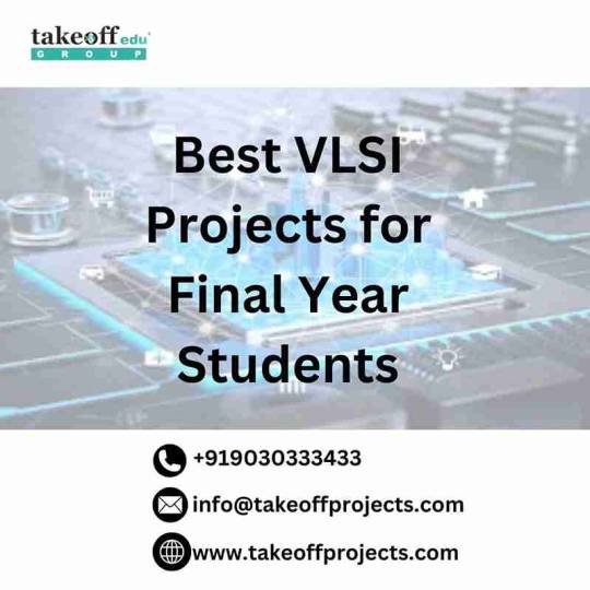
Best VLSI Projects for Final Year Students
Here are some great VLSI project ideas for final-year students:
1. Image Processing System on FPGA: Algorithm, such as edge detection or image filtering should be performed through the usage of FPGAs for optimal performance.
2. Low-Power SRAM Design: Design and simulate a low-power Static Random Access Memory (SRAM) cell, targetting leakage and dynamic power dissipation.
3. Digital Signal Processor (DSP) Design: Design an example of a DSP that will allow a specific signal to be filtered or, for instance, undergo FFT.
4. Wireless Sensor Network (WSN) Protocol Implementation: Devise a VLSI based sensor node for wireless communication that will support protocols used in data transmission.
5. Reconfigurable Hardware Architecture: It is necessary to elaborate a box which is able to evolve in order to support several applications: in this context, it is possible to try to reconfigure parts of the hardware during the runtime according to the specific needs of the client application.
6. Cryptographic Hardware Accelerator: Propose and design a device for which you could use cryptographic algorithms or primitives including AES or RSA where optimization of both speed optimization and security is important.
7. System-on-Chip (SoC) Design: Selected h/w architects use Verilog or VHDL to design a including microcontroller, memory and other peripherals.
8. Artificial Neural Network (ANN) on FPGA: Devise a mini ANN for image recognition and other related work and optimally use the features of parallel processing provisioned by FPGAs.9. Automated VLSI Testing Tool: Design a testing and validation software system that has reduced time and eliminated errors in conducting tests of VLSI designs (Very Large Scale Integration).
10. Temperature Sensor with Data Logger: It will be a VLSI (Very Large Scale Integration) chip for measuring temperature and recording data, with the capability to display the data on a PC or a mobile connection.
All these project proposals present prospects to learn diverse aspects of VLSI design and implementation in addition to enhancing creativity. Choose one that you are interested in and which you can afford to do!
#vlsi#finalyear#verylargescaleintegration#VLSIDesign#engineeringstudents#studentsprojects#takeoffedugroup#takeoffprojects
0 notes
Text
Understanding FPGA Architecture: Key Insights
Introduction to FPGA Architecture
Imagine having a circuit board that you could rewire and reconfigure as many times as you want. This adaptability is exactly what FPGAs offer. The world of electronics often seems complex and intimidating, but understanding FPGA architecture is simpler than you think. Let’s break it down step by step, making it easy for anyone to grasp the key concepts.
What Is an FPGA?
An FPGA, or Field Programmable Gate Array, is a type of integrated circuit that allows users to configure its hardware after manufacturing. Unlike traditional microcontrollers or processors that have fixed functionalities, FPGAs are highly flexible. You can think of them as a blank canvas for electrical circuits, ready to be customized according to your specific needs.
How FPGAs Are Different from CPUs and GPUs
You might wonder how FPGAs compare to CPUs or GPUs, which are more common in everyday devices like computers and gaming consoles. While CPUs are designed to handle general-purpose tasks and GPUs excel at parallel processing, FPGAs stand out because of their configurability. They don’t run pre-defined instructions like CPUs; instead, you configure the hardware directly to perform tasks efficiently.
Basic Building Blocks of an FPGA
To understand how an FPGA works, it’s important to know its basic components. FPGAs are made up of:
Programmable Logic Blocks (PLBs): These are the “brains” of the FPGA, where the logic functions are implemented.
Interconnects: These are the wires that connect the logic blocks.
Input/Output (I/O) blocks: These allow the FPGA to communicate with external devices.
These elements work together to create a flexible platform that can be customized for various applications.
Understanding Programmable Logic Blocks (PLBs)
The heart of an FPGA lies in its programmable logic blocks. These blocks contain the resources needed to implement logic functions, which are essentially the basic operations of any electronic circuit. In an FPGA, PLBs are programmed using hardware description languages (HDLs) like VHDL or Verilog, enabling users to specify how the FPGA should behave for their particular application.
What are Look-Up Tables (LUTs)?
Look-Up Tables (LUTs) are a critical component of the PLBs. Think of them as small memory units that can store predefined outputs for different input combinations. LUTs enable FPGAs to quickly execute logic operations by “looking up” the result of a computation rather than calculating it in real-time. This speeds up performance, making FPGAs efficient at performing complex tasks.
The Role of Flip-Flops in FPGA Architecture
Flip-flops are another essential building block within FPGAs. They are used for storing individual bits of data, which is crucial in sequential logic circuits. By storing and holding values, flip-flops help the FPGA maintain states and execute tasks in a particular order.
Routing and Interconnects: The Backbone of FPGAs
Routing and interconnects within an FPGA are akin to the nervous system in a human body, transmitting signals between different logic blocks. Without this network of connections, the logic blocks would be isolated and unable to communicate, making the FPGA useless. Routing ensures that signals flow correctly from one part of the FPGA to another, enabling the chip to perform coordinated functions.
Why are FPGAs So Versatile?
One of the standout features of FPGAs is their versatility. Whether you're building a 5G communication system, an advanced AI model, or a simple motor controller, an FPGA can be tailored to meet the exact requirements of your application. This versatility stems from the fact that FPGAs can be reprogrammed even after they are deployed, unlike traditional chips that are designed for one specific task.
FPGA Configuration: How Does It Work?
FPGAs are configured through a process called “programming” or “configuration.” This is typically done using a hardware description language like Verilog or VHDL, which allows engineers to specify the desired behavior of the FPGA. Once programmed, the FPGA configures its internal circuitry to match the logic defined in the code, essentially creating a custom-built processor for that particular application.
Real-World Applications of FPGAs
FPGAs are used in a wide range of industries, including:
Telecommunications: FPGAs play a crucial role in 5G networks, enabling fast data processing and efficient signal transmission.
Automotive: In modern vehicles, FPGAs are used for advanced driver assistance systems (ADAS), real-time image processing, and autonomous driving technologies.
Consumer Electronics: From smart TVs to gaming consoles, FPGAs are used to optimize performance in various devices.
Healthcare: Medical devices, such as MRI machines, use FPGAs for real-time image processing and data analysis.
FPGAs vs. ASICs: What’s the Difference?
FPGAs and ASICs (Application-Specific Integrated Circuits) are often compared because they both offer customizable hardware solutions. The key difference is that ASICs are custom-built for a specific task and cannot be reprogrammed after they are manufactured. FPGAs, on the other hand, offer the flexibility of being reconfigurable, making them a more versatile option for many applications.
Benefits of Using FPGAs
There are several benefits to using FPGAs, including:
Flexibility: FPGAs can be reprogrammed even after deployment, making them ideal for applications that may evolve over time.
Parallel Processing: FPGAs excel at performing multiple tasks simultaneously, making them faster for certain operations than CPUs or GPUs.
Customization: FPGAs allow for highly customized solutions, tailored to the specific needs of a project.
Challenges in FPGA Design
While FPGAs offer many advantages, they also come with some challenges:
Complexity: Designing an FPGA requires specialized knowledge of hardware description languages and digital logic.
Cost: FPGAs can be more expensive than traditional microprocessors, especially for small-scale applications.
Power Consumption: FPGAs can consume more power compared to ASICs, especially in high-performance applications.
Conclusion
Understanding FPGA architecture is crucial for anyone interested in modern electronics. These devices provide unmatched flexibility and performance in a variety of industries, from telecommunications to healthcare. Whether you're a tech enthusiast or someone looking to learn more about cutting-edge technology, FPGAs offer a fascinating glimpse into the future of computing.
0 notes
Text
Intel’s Silicon Mobility OLEA U310 SoC Boosts EV Progress
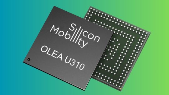
Silicon Mobility OLEA U310
One of the main obstacles to purchasing an electric vehicle (EV) is still its expensive cost, which deters many prospective consumers worldwide. Due in large part to the high expense of developing improved battery and e-motor technologies, electric vehicles (EVs) are now more expensive to construct than conventional gasoline-powered vehicles. Improving the efficiency of current battery technology at the vehicle level through energy savings and better interaction with EV station infrastructure is the short-term solution.
With the release of the new OLEA U310 system-on-chip (SoC) today, Silicon Mobility, an Intel company, has successfully addressed this precise difficulty. The entire performance of electric cars (EVs) will be greatly enhanced by this next-generation technology, which will also expedite the design and production processes and expand SoC services to guarantee smooth operation across a variety of EV station platforms.
Mobility in Silicon
The new SoC, which is a first for the industry, is the first all-in-one solution that combines software and hardware, and it is designed to meet the requirements of distributed software-based electrical architectures for powertrain domain control. With its distinct hybrid and heterogeneous architecture, the OLEA 310 FPCU can take the place of up to six conventional microcontrollers in a system configuration that includes an on-board charger, a gearbox, an inverter, a motor, and a DC-DC converter. Original equipment manufacturers (OEMs) and Tier 1 suppliers can regulate a variety of power and energy functions simultaneously and in real time with the 310 FPCU.
Create a function grouping for your e-powertrain
The OLEA U310 is a recent addition to the Silicon Mobility FPCU line. Its design matches distributed software requirements for powertrain domain control in electrical/electronic designs. Beyond the capabilities of conventional microcontrollers, the OLEA U310 is constructed with a novel hybrid and heterogeneous architecture that embeds numerous software and hardware programmable processing and control units seamlessly integrating functional safety and the cybersecurity into its fundamental design. It hosts and connects, on a single chip, the essential event-based multifunction control requirements with the time-based and multitask software application needs.
Created with the newest demands in automobile control in mind
The OLEA U310 can do more than only powertrain tasks. Additional uses for this adaptable system-on-a-chip include:
Systems for Chassis Control
Fusion of Data
Compressor air
System for Thermal Management
Different Control Mechanisms
EV makers may create a more integrated and effective control system that improves control and performance by utilising the adaptability of the OLEA U310.
Authority of the AxEC
For direct sensor and actuator interfacing, the Advanced eXecution & Event Control (AxEC) unit integrates programmable hardware, mathematical coprocessors, and adjustable peripherals. The core of the FPCU architecture is the programmable hardware known as the Flexible Logic Units (FLU). It is a programmable logic fabric that can be designed using common hardware description languages like Verilog or VHDL. It is furnished with flip-flops, SRAM, lookup tables, and signal processing units. 1-4 FLU partitions are a notion that is introduced by the OLEA U Series.
CPUs are in charge of high-level and low-response-time software, while AxEC deals with real-time control and fast-response processing. For particular jobs, designers have the option of using CPU or AxEC; nevertheless, AxEC usually performs sophisticated processing, minimising CPU utilisation. Regardless of the number or frequency of events, hardware processing guarantees prompt, accurate responses.
Protected by OLEA SiLant
The greatest level of automotive safety integrity specified by the ISO 26262 functional safety standard, ASIL-D design ready, is met by the FPCU. The OLEA U Series Safety Integrity Agent (SiLant) is in charge of identifying, containing, and responding to errors in nanoseconds. It is the key hub for all safety measures integrated within the FPCU. SiLant detects software and system faults in addition to latent and transient faults at the semiconductor level.
OLEA U FLU provides safe multitasking and function grouping with unified firmware virtualization from CPU down to FLU level with the advent of multi-CPU and multi-FLU. OLEA U offers assurances and a deterministic architecture. Worst-Scene Performance It’s time to create applications that require safety.
Protected by OLEA FHSM
For the best defence against current and potential threats, the latest generation of FPCU is available. A subsystem integrated into the OLEA U Series that complies with the ISO 21434 automotive cybersecurity standard and EVITA Full is called the Flexible Hardware Security Module (FHSM). Its specialised programmable hardware allows it to contain hardware-accelerated security functions that can be used to improve protection or keep an eye out for any system security breaches. This special feature makes use of a wider range of cryptographic techniques to enable safe real-time communications as well as secure software updates and execution.
Mobility of Silicon
Together with the bill of material (BoM) reduction, preliminary data indicates that compared to current EVs, there will be a 5% increase in energy efficiency, a 25% reduction in motor size for the same power, a 35% decrease in cooling requirements, and a 30% reduction in passive component size. With fewer components to incorporate, the new Silicon Mobility technology enables EV makers to develop software-defined electric vehicles with superior performance, increased range, and potentially cheaper production costs. The industry’s transition to an all-electric and software-defined future will be accelerated by the new solution, which also enhances Intel Automotive’s current line of AI-enhanced software-defined vehicle (SDV) SoCs.
Silicon Mobility OLEA U310 Features
2nd generation of FPCU
3x Cortex-R52 @ 350MHz – 2196 DMIPS
AxEC 2.0: 2x FLUs @ 175Mhz – 400 GOPS + 9.1 GMAC
SILant 2.0: Safe and Determinist Multi-Core/FLU
Flexible HSM: HW & SW EVITA Full
8MB of P-Flash, 256kB of D-Flash, 1MB of SRAM
CAN FD, CAN XL, Ethernet
ISO/SAE 21434 certifieISO 26262 ASIL-D & ISO/SAE 21434 compliant
AEC-Q100 Grade 1
292 BGA
Read more on Govindhtech.com
0 notes
Text
NO.1 VLSI System Design in India
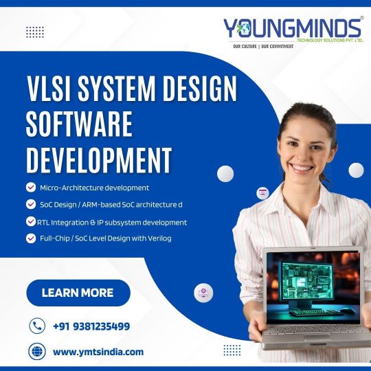
Welcome to Youngminds Technology Solutions, a leading VLSI System Design Software Development Agency in India. Our focus is on the development of the latest solutions that promote innovation and efficiency in the area of VLSI system design. Come with us as we are building the future of technology together.
Our VLSI design team has deep expertise in realizing product and software development for a wide range of application areas on cutting-edge technologies. YMTS team have wide set of skills across electronic chip design flow from specification to GDSII on latest node technologies, with special focus on RTL/FPGA Design, design verification and FPGA emulation.
VLSI SYSTEM DESIGN ASIC / FPGA Design Development
Design is not just what it looks like and feels like. Design is how it works.” You can hire us to build your custom website that fulfils your unique requirements. Unlike using a pre-built template for your site, a customized website is specifically created for you.
VLSI Services our Engineering team expertise in various stages of the design flow, Such as:
Micro-Architecture development for given specifications
SoC Design / ARM-based SoC architecture designs
RTL Integration & IP subsystem development
Full-Chip / SoC Level Design with Verilog, VHDL, System Verilog
Migration from FPGA to ASIC
Lint, CDC Checks and writing waivers
Integration of digital and analogue blocks (Like SERDES PMA + PCS or DDR + Phy etc.,)
Synthesis, STA Constraints for both ASIC and FPGA
Logic equivalency and formality checks
Hands-on experience on Various Industrial EDA tools
Optimization of Power, Area and timing trade off
FPGA Prototyping on Xilinx / Altera FPGA Boards
Optimization & Maintenance
We are here to help you understand the importance of web application maintenance. We provide several services which will enable your web application run error-free and smooth.
Our knowledge-based AI platform driven by automation and innovation. It enables our clients’ businesses to continuously reinvent system landscapes and achieve IT goals that align with business needs. By aligning IT with business value, we help clients push the envelope beyond cost and quality.
Training
YMTS provides training programs that help students / Engineers and customers get to productivity faster. All our training programs have been developed keeping in mind what it takes to accelerate skill development of today's R&D engineers and have been proven in-house with our own new hires as well as multiple customers.
As a top VLSI System Design Software Development Services, we are proud of the excellent services we offer. Our knowledge and dedication assure the best solutions for your VLSI requirements. Select us for the best performance in the VLSI system design. Visit More Information: https://ymtsindia.com/vlsi-system-design Meta Tags: VLSI System Design, VLSI System Management, VLSI Design Services, VLSI System Design Agency
0 notes
Text
EP4CE15F23I7N
Unveiling the Power of the Intel EP4CE15F23I7N FPGA
Introduction:
The Intel EP4CE15F23I7N FPGA represents a pinnacle of programmable logic technology, offering unparalleled performance, versatility, and scalability. As a cornerstone in various electronic systems, this FPGA empowers engineers and developers to implement complex functionalities, accelerate time-to-market, and address diverse application requirements. In this comprehensive guide, we'll delve into the features, applications, and development process associated with the Intel EP4CE15F23I7N FPGA.
Understanding the Intel EP4CE15F23I7N FPGA:
At the heart of the Intel EP4CE15F23I7N lies a sophisticated architecture optimized for a myriad of tasks, ranging from embedded systems to high-performance computing.
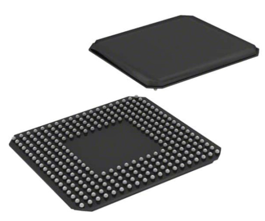
Architecture Overview:
The Intel EP4CE15F23I7N boasts a rich assortment of resources, including programmable logic elements, embedded memory blocks, high-speed transceivers, and dedicated input/output (I/O) pins. This flexible architecture enables designers to implement complex algorithms, signal processing chains, and control systems with precision and efficiency.
Key Features:
With features such as hardened processors, configurable DSP blocks, and advanced clocking resources, the EP4CE15F23I7N offers unparalleled flexibility and performance. These features are instrumental in meeting the demanding requirements of modern applications, including machine learning, image processing, and network acceleration.
Development Process:
To fully leverage the capabilities of the Intel EP4CE15F23I7N FPGA, developers must navigate through the stages of design, implementation, and validation with diligence and proficiency.
Design Entry:
Design entry can be accomplished using hardware description languages (HDL) such as Verilog or VHDL, or through graphical schematic entry tools. Intel's Quartus Prime Design Software provides a comprehensive platform for design entry, synthesis, and verification.
Synthesis and Optimization:
During synthesis, the HDL code is translated into a hardware netlist, which is then optimized for performance, area, and power consumption. Quartus Prime's synthesis and optimization tools enable designers to achieve the desired balance between these metrics while meeting stringent timing constraints.
Place and Route:
The place and route stage involves mapping the logical design onto physical FPGA resources and determining the routing of interconnections. Quartus Prime's advanced algorithms ensure optimal placement and routing, thereby maximizing performance and minimizing timing violations.
Testing and Validation:
Thorough testing and validation are imperative to ensure the reliability and functionality of the FPGA design.
Functional Simulation:
Functional simulation allows designers to verify the behavior of the FPGA design under different operating conditions and input stimuli. Comprehensive test benches and simulation tools facilitate rigorous testing and debugging.
Hardware Validation:
Once the design is synthesized, implemented, and verified through simulation, it is deployed onto a target FPGA device for hardware validation. Real-world testing validates the performance and functionality of the FPGA design in practical scenarios.
Conclusion:
The Intel EP4CE15F23I7N FPGA stands as a testament to innovation and engineering excellence, offering unmatched performance, versatility, and scalability. By mastering its architecture and development workflow, designers can unlock its full potential and realize groundbreaking solutions across diverse industries. Whether you're designing cutting-edge data processing systems, high-speed communication interfaces, or embedded control applications, the Intel EP4CE15F23I7N FPGA serves as a reliable and powerful enabler of technological advancement.
1 note
·
View note
Text
FPGA System Design Training - VLSI Guru
In the evolving world of digital design, FPGA System Design Training has become a cornerstone for engineers aspiring to excel in hardware design and embedded systems. VLSI Guru’s comprehensive FPGA System Design course equips you with the skills to design, develop, and implement FPGA-based systems using the latest industry tools and methodologies.
What is FPGA System Design?
FPGA (Field-Programmable Gate Array) System Design involves programming configurable logic blocks to create customized hardware solutions. FPGAs are widely used in applications like embedded systems, signal processing, and high-performance computing due to their flexibility, scalability, and speed.
Why Choose VLSI Guru for FPGA System Design Training?
1. Industry-Focused Curriculum
VLSI Guru’s training covers all essential aspects of FPGA System Design, including:
Basics of FPGA architecture and design flow.
Programming using VHDL and Verilog.
Advanced concepts like timing analysis, IP integration, and system optimization.
Hands-on experience with industry tools like Xilinx Vivado and Intel Quartus.
2. Hands-On Learning
Our training emphasizes practical exposure, allowing you to work on real-world FPGA projects such as:
Designing digital circuits.
Implementing communication protocols.
Developing hardware acceleration modules.
3. Expert Mentorship
Learn from experienced trainers with extensive industry expertise, ensuring you gain insights into real-world FPGA system design challenges and solutions.
4. Placement Assistance
VLSI Guru provides job-oriented training along with resume building, interview preparation, and placement support to help you secure roles in top hardware and semiconductor companies.
What Will You Learn?
Fundamentals of FPGA architecture and HDL programming.
Design, simulation, and implementation using Verilog/VHDL.
Prototyping on FPGA development boards.
Debugging and optimization techniques for FPGA-based systems.
Who Should Enroll?
This course is ideal for:
Engineering graduates in electronics, electrical, or related fields.
Freshers and professionals seeking a career in FPGA System Design.
Embedded system developers looking to enhance their hardware design skills.
Why FPGA System Design is in Demand
FPGAs are the backbone of modern electronics, powering innovations in telecommunications, automotive, IoT, and artificial intelligence. Skilled FPGA engineers are in high demand to meet the growing need for customized hardware solutions.
Join VLSI Guru Today
Get ahead in the competitive semiconductor industry with VLSI Guru’s FPGA System Design Training. Our hands-on approach, expert guidance, and career support ensure you are ready to tackle the challenges of FPGA-based system design.
Contact us now to learn more and take the first step toward an exciting career in FPGA design
0 notes
Text
High Performance FPGA Solutions

In today's rapidly evolving technological landscape, the demand for high-performance solutions is ever-increasing. Field-Programmable Gate Arrays (FPGAs) have emerged as versatile tools offering customizable hardware acceleration for a wide range of applications. Let's delve into the world of high performance FPGA solutions, exploring their key features, applications, challenges, recent advances, case studies, and future trends.
Introduction to High Performance FPGA Solutions
Definition of FPGA
Field-Programmable Gate Arrays (FPGAs) are semiconductor devices that contain an array of programmable logic blocks and configurable interconnects. Unlike Application-Specific Integrated Circuits (ASICs), FPGAs can be programmed and reprogrammed after manufacturing, allowing for flexibility and customization.
Importance of High Performance in FPGA Solutions
High performance is crucial in FPGA solutions to meet the demanding requirements of modern applications such as real-time data processing, artificial intelligence, and high-frequency trading. Achieving optimal speed, throughput, and efficiency is paramount for maximizing the effectiveness of FPGA-based systems.
Key Features of High Performance FPGA Solutions
Speed and Throughput
High performance FPGA solutions are capable of executing complex algorithms and processing vast amounts of data with exceptional speed and efficiency. This enables real-time decision-making and rapid response to dynamic inputs.
Low Latency
Reducing latency is essential in applications where response time is critical, such as financial trading or telecommunications. High performance FPGAs minimize latency by optimizing data paths and processing pipelines.
Power Efficiency
Despite their high performance capabilities, FPGA solutions are designed to operate within strict power constraints. Advanced power management techniques ensure optimal performance while minimizing energy consumption, making FPGAs suitable for battery-powered or energy-efficient devices.
Flexibility and Reconfigurability
One of the key advantages of FPGAs is their inherent flexibility and reconfigurability. High performance FPGA solutions can adapt to changing requirements by reprogramming the hardware on-the-fly, eliminating the need for costly hardware upgrades or redesigns.
Applications of High Performance FPGA Solutions
Data Processing and Analytics
FPGAs excel in parallel processing tasks, making them ideal for accelerating data-intensive applications such as big data analytics, database management, and signal processing.
Artificial Intelligence and Machine Learning
The parallel processing architecture of FPGAs is well-suited for accelerating AI and ML workloads, including model training, inference, and optimization. FPGAs offer high throughput and low latency, enabling real-time AI applications in edge devices and data centers.
High-Frequency Trading
In the fast-paced world of financial markets, microseconds can make the difference between profit and loss. High performance FPGA solutions are used to execute complex trading algorithms with minimal latency, providing traders with a competitive edge.
Network Acceleration
FPGAs are deployed in network infrastructure to accelerate packet processing, routing, and security tasks. By offloading these functions to FPGA-based accelerators, network performance and scalability can be significantly improved.
Challenges in Designing High Performance FPGA Solutions
Complexity of Design
Designing high performance FPGA solutions requires expertise in hardware architecture, digital signal processing, and programming languages such as Verilog or VHDL. Optimizing performance while meeting timing and resource constraints can be challenging and time-consuming.
Optimization for Specific Tasks
FPGAs offer a high degree of customization, but optimizing performance for specific tasks requires in-depth knowledge of the application domain and hardware architecture. Balancing trade-offs between speed, resource utilization, and power consumption is essential for achieving optimal results.
Integration with Existing Systems
Integrating FPGA-based accelerators into existing hardware and software ecosystems can pose compatibility and interoperability challenges. Seamless integration requires robust communication protocols, drivers, and software interfaces.
Recent Advances in High Performance FPGA Solutions
Improved Architectures
Advancements in FPGA architecture, such as larger logic capacity, faster interconnects, and specialized processing units, have led to significant improvements in performance and efficiency.
Enhanced Programming Tools
New development tools and methodologies simplify the design process and improve productivity for FPGA developers. High-level synthesis (HLS) tools enable software engineers to leverage FPGA acceleration without requiring expertise in hardware design.
Integration with Other Technologies
FPGAs are increasingly being integrated with other technologies such as CPUs, GPUs, and ASICs to create heterogeneous computing platforms. This allows for efficient partitioning of tasks and optimization of performance across different hardware components.
Case Studies of Successful Implementation
Aerospace and Defense
High performance FPGA solutions are widely used in aerospace and defense applications for tasks such as radar signal processing, image recognition, and autonomous navigation. Their reliability, flexibility, and performance make them ideal for mission-critical systems.
Telecommunications
Telecommunications companies leverage high performance FPGA solutions to accelerate packet processing, network optimization, and protocol implementation. FPGAs enable faster data transfer rates, improved quality of service, and enhanced security in telecommunication networks.
Financial Services
In the highly competitive world of financial services, microseconds can translate into significant profits or losses. High performance FPGA solutions are deployed in algorithmic trading, risk management, and low-latency trading systems to gain a competitive edge in the market.
Future Trends in High Performance FPGA Solutions
Increased Integration with AI and ML
FPGAs will play a vital role in accelerating AI and ML workloads in the future, especially in edge computing environments where low latency and real-time processing are critical.
Expansion into Edge Computing
As the Internet of Things (IoT) continues to grow, there will be increasing demand for high performance computing at the edge of the network. FPGAs offer a compelling solution for edge computing applications due to their flexibility, efficiency, and low power consumption.
Growth in IoT Applications
FPGAs will find widespread adoption in IoT applications such as smart sensors, industrial automation, and autonomous vehicles. Their ability to handle diverse workloads, adapt to changing requirements, and integrate with sensor networks makes them an ideal choice for IoT deployments.
Conclusion
In conclusion, high performance FPGA solutions play a crucial role in driving innovation and accelerating the development of advanced technologies. With their unparalleled speed, flexibility, and efficiency, FPGAs enable a wide range of applications across industries such as aerospace, telecommunications, finance, and IoT. As technology continues to evolve, the demand for high performance FPGA solutions will only continue to grow, shaping the future of computing.
0 notes
Text
youtube
VHDL Basics : Begin the World of FPGA Design Tools & VHDL Design Flow
Welcome to our comprehensive guide on FPGA design tools and VHDL design flow! In this video, we dive into the fascinating world of FPGA design and explore the essential tools and methodologies needed for successful FPGA development. Whether you're a beginner or an experienced engineer, this tutorial will provide valuable insights and tips to enhance your FPGA design skills. We start by introducing the fundamentals of FPGA design, explaining the benefits and versatility of using FPGAs in various applications. From there, we explore the wide range of design tools available, from popular industry-standard software like Xilinx Vivado and Altera Quartus Prime to open-source alternatives like GHDL and Icarus Verilog. We highlight the strengths and features of each toolset, enabling you to choose the most suitable one for your projects. With a solid foundation in FPGA design and tools, we then delve into the VHDL (VHSIC Hardware Description Language) design flow. From understanding the basics of VHDL syntax to implementing complex digital designs, we provide step-by-step explanations and practical demonstrations. You'll learn about entity and architecture design, the importance of libraries, and how to simulate and synthesize VHDL code for your FPGA. To ensure a holistic learning experience, we discuss common challenges and pitfalls in FPGA design and provide valuable troubleshooting tips. We also touch upon advanced topics like FPGA optimization techniques, timing analysis, and physical implementation considerations. So, whether you're a student, hobbyist, or professional looking to enhance your FPGA design skills, this tutorial is the ultimate resource to get started on your journey. Join us now and unlock the vast potential of FPGA design tools and the VHDL design flow! FPGA design tools, VHDL design flow, FPGA development, Xilinx Vivado, Altera Quartus Prime, VHDL, Verilog, VHDL syntax, digital design, entity architecture, libraries, simulate VHDL code, synthesize VHDL code, FPGA optimization techniques, timing analysis, physical implementation, FPGA design skills.
Subscribe to "Learn And Grow Community"
YouTube : https://www.youtube.com/@LearnAndGrowCommunity
LinkedIn Group : https://www.linkedin.com/groups/7478922/
Blog : https://LearnAndGrowCommunity.blogspot.com/
Facebook : https://www.facebook.com/JoinLearnAndGrowCommunity/
Twitter Handle : https://twitter.com/LNG_Community
DailyMotion : https://www.dailymotion.com/LearnAndGrowCommunity
Instagram Handle : https://www.instagram.com/LearnAndGrowCommunity/
Follow #LearnAndGrowCommunity
#HDL Design#Digital Design#Verilog#VHDL#FPGA#Simulation#Synthesis#B.Tech#VLSI#Training#Career#ASIC#Xilinx#Students#hardware description language#VHDL tutorial#VHDL beginner guide#VHDL syntax#VHDL data types#VHDL modeling#behavioral modeling#data flow modeling#FSM#FPGA design tools#VHDL design flow#FPGA development#Xilinx Vivado#Altera Quartus Prime#entity#architecture
1 note
·
View note
Text
COMP4300 Lab Exercise One solved
Objective This lab is aimed at getting you familiar with using the ModelSim simulator. The circuits you will be simulating should be familiar to you from ELEC2200. Instructions Write a VHDL program consisting of a single entity whose architecture is a single process that implements a one-bit full adder . That is, a circuit which behaves as specified in the following truth table. You…
0 notes