#amec
Explore tagged Tumblr posts
Visit Tumblr Blog
Explore Tumblr blogs with no restrictions, modern design and the best experience.
Last Seen Tumblr Blogs


Fun Fact
There are dozens of funny blogs to kill time on Tumblr.
Text

Asociación Malagueña de Enología y Cata. Segunda sesión de cata, en este caso maridada, de vinos generosos de Bodegas Barbadillo a cargo de D. Manuel Domínguez quimico emérito y consejero de la bodega. Catamos en los tres casos un vino de encabezado y el producto terminado. Amontillado Principe, 19,5 % Vol. Maridado con canapé de salmón ahumado y garbanzos con espinacas. Oloroso Cuco Dry, 18,5 % Vol. Maridado con queso viejo y pollo al curry. Palo Cortao Obispo Gascón, 21 % Vol. Maridado con croqueta de puchero y crema de setas. Se encargaron de la preparación y servicio del maridaje nuestras directivas, Consuelo Martín, María y Gloria Sánchez. #Amec #amecvinos #bodegasbarbadillo #dojerez #jerez #sherry #xeres #amontilladoprincipe #olorosocuco #palocortaoobispogascon
#amecvinos#amec#bodegasbarbadillo#dojerez#jerez#xeres#sherry#amontilladoprincipe#olorosocuco#palocortaoobispogascon
0 notes
Text
Merayakan 10 Muharram 1445 H Sekolah AMEC Berbagi Dengan Puluhan Anak Yatim
dapurremaja|Pondok Petir Sekolah Islam Al Mamun Education Center (AMEC) kelurahan Serua kecamatan Bojongsari, merayakan Idhul Yatama atau hari Asyuro, 10 Muharram 1445 H tahun 2023 kegiatan yang disisi dengan santunan dan jamuan makan siang bersama anak-anak Yatim Piatu dan dhuafa. Continue reading Untitled

View On WordPress
0 notes
Text

As stars and other notables of yesterday mingled with today's great to help Irving Cummings celebrate his 30th year in the motion picture industry at a dinner in honor of the director at 20th Century-Fox where he is now under contract.
From the upper left: Francis Powers, Cummings, Don Ameche, Alice Faye, Buster Keaton, Rosemary Thebe, Stuart Holms and Chester Conklin. In the right foreground are Director Mal St. Clair and Ben Turpin.
#buster keaton#1930s#1910s#1920s#1920s hollywood#silent film#silent comedy#silent cinema#silent era#silent movies#pre code#pre code hollywood#pre code film#pre code era#pre code movies#damfino#damfinos#vintage hollywood#black and white#buster edit#old hollywood#slapstick#alice faye#francis powers#irving cummings#don amece#rosemary thebe#stuart holms#chester conklin#mal st clair
16 notes
·
View notes
Text


Awet Aleu by Amec Elzey for Schon Magazine May 2025
245 notes
·
View notes
Text
Every year I post about how powerful the Annual Medical Education Conference is. And every year, like clockwork, the hate rolls in. Because some people are still threatened by the imagery of Black doctors.
That’s exactly why spaces like AMEC matters. It’s a celebration of diversity in medicine, in spite of the pushback.
These moments are reminders: we’re not done. We can’t be. Because the future of healthcare depends on what we build today.
45 notes
·
View notes
Text
「宮崎正弘の国際情勢解題」
令和七年(2025年)2月8日(土曜日)弐
通巻第8642号
ハイテク技術が如何にして中国へ渡ったのか
台湾企業のエンジニア多数が中国企業に転職していた
*************************
不倫小説にでてきそうな修飾語は「爛れる」「ぐじょぐじょ」
「ディープシーク・ショッ」クの前はファーウェイ(華為技術)のショック。いずれにしても禁輸対象の高性能半導体、集積回路を中国が入手していたことだ。デイ-プシークは既に5万個のNvidia H100チップを保有している(QQ、2024年3月14日)
オランダと日本の半導体製造装置がなければ中国が製造できるはずがないのに、如何にして彼らは、これらハイテク半導体を入手できたのか?
筆者がこれまでにも指摘したように韓国、台湾、そして日本から技術者が高給に釣られて中国企業に引き抜かれた。
もうひとつが第三国経由での迂回輸入である。韓国、台湾の半導体が、インド、マレーシア、シンガポールあたりで「抜け道の倉庫」となっている。
TSMCは次世代のハイテクを台湾で製造すると宣言している。エヌビディアもその意向である。日本にTSMC工場が稼働しているが、ここは40ナノと28ナノ、電化製品と自動車、スマホ用である。中国はとうにこれらのレベルには追いつき、SMICなどは自給できる。
米国はTSMCに対して、最先端半導体をアラバマ州で製造するように要請し、バイデン政権は巨額の補助金をつけた。TSMCのアラバマ工場は年内稼働予定である。
日本が官民挙げて製造する2ナノは北海道千歳のラピダスで、はやければ2026年に製造が始まる。
さらに懸念材料はTSMC はその他の国々や地域に工場を設立しているが、多くは米国よりも中国との関係が深いことである。
TSMCは中国にとって重要なターゲットなのである。
北京は欲しい技術を手に入れるために合法・非合法を問わず、巧妙な手段を講じてきた長い歴史がある。そもそもTSMSの中国における製造工場と、中国の大手企業間では人材の流動がある。台湾の半導体メーカー多数は中国に拠点を置いている。
1990年代のモトローラを皮切りにインテル、サムスン、SKハイニックス、UMCが深セン、蘇州、西安、大連、成都、厦門などの都市に工場を建設した TSMCの上海工場は200mmウェハを生産する前工程工場である。南京工場は、2018年半ばに300mmウェハの生産を開始した。
後者は、中国で最も先進的なラインである。
これらTSMC の中国の工場と、中国企業が所有する工場との間で、エンジニアやサポート要員の大規模な移動が行われている。
つまりハイテク技術は筒抜けなのである。
▼台湾技術者は開発競争マインドはあっても愛国心は希薄なのか?
よりによってTSMCとファウェイ間に頻繁な事異動が行われていた。
中国の電話番号とクレジットカードが必要なMaiMaiの有料アカ��ントがなくても、R&Dエンジニアリング、エッチング、フォトリソグラフィー、歩留まりエンジニアリングなどの技術職に就いている元TSMCの専門家やエキスパートが何十人もいる。
人材市場では、孫一超などのHuaweiの元人事採用担当者がTSMCの中国工場で働いていることも判明している。
元TSMCのエンジニアや技術専門家は、米国政府の制裁下にある中国の大手企業数社にも在籍している。これらには、CXMT(長金存儲科技)、YMTC(長江存儲科技)、AMEC(中微半導体設盤)などだ。
TSMCのエンジニアが制裁対象の中国企業に移籍するほか、TSMCの元高官が台湾での職を離れ、中国で働き、あるいは関連事業を手がけている。ラムリサーチで25年以上の経験を持つフォトリソグラフィーとエッチングの専門家、林政助は2024年6月に「安徽芯泉半導体」のCEOに就任した。拙著にも書いたが、SMIC(中芯国際)を設立した張汝京はTSMCの元役員であり、2000年に中国本土に渡った。
まさに「不倫小説」を連想した。
19 notes
·
View notes
Text


Awet Aleu by Amec Elzey for Schon Magazine May 2025
7 notes
·
View notes
Text
TCW Rewatch: Season 2 Episodes 12-15
The dreaded mandalore arc post. Im going to be upfront, if you dont like me slandering Satine just dont even read the post. Turn back now. I’m not going to engage in dumb arguments. If you want to comment be civil.
I try to be as objective as I can writing these. I call it as I see it even when i do like the character. However I also recognize the tone can come across as aggressive, its not meant to be I just Talk Like That.
Anyways, enjoy!
Episode 12: The Mandalore Plot
* Obi wan sent to Mandalore to investigate rumors about a secret army built for the separatists
* “All of our warriors were exiled to concordia. They died out years ago” thats fucking weird. Like if we’re talking just Death Watch thatd be whatever they’re terrorists but all of the warriors?? What about Satine’s Guard? Do they not qualify as warriors? Or are they allowed because they’re Satine’s warriors
* Amec awfully defensive about Jango Fett being mandalorian. “Jango Fett was a common bounty hunter. How he acquired that armor is beyond me” what exactly makes someone Mandalorian or not?
* Satine is so hostile just as soon as she enters. That doesnt look good for your case, Duchess, considering you want to prove you have no intent of turning against the Republic. bad political decision.
* Sabateur is mandalorian. Amec really going hard on the denial "no mandalorian would engage in such violence. not anymore" babe you have Video Evidence of the exact opposite
* Satine assumes this whole thing is because the Senate wants to intervene in the affairs of Mandalore
* wild assumption considering obi wan has done nothing thusfar outside of try to get answers for his investigation. awfully presumtuous and honestly arrogant all things considered
* get her ass, kenobi
* i find it so hard to believe these two are supposed to have been in love
* Ok so now you mention Death Watch, not earlier when you were throwing around baseless accusations where that information could have been necessary??
* "its hardly a movement" a small group of hooligans typically doesnt warrant secret officials rooting them out. all this tells me is that she knows about death watch and refuses to do much of anything ab it. what does she plan to do with the investigation?
* The separatists want to help overthrow satine
* Satine trying to lecture Obi Wan on peacekeeping and Jedi ideals is fucking audacious. “The job of a peacekeeper is to make sure that conflict does not arise” and what when conflict does? You cant always prevent conflict. The conflict is already there so arguably Obi Wan has a more understandable and realistic point of view here.
* Also terribly ironic that an act of terrorism occurs as they are having this conversation. This isn’t Peace. Its ignorance.
* “Hooligans couldnt have arranged an attack of this scale” “It must be an offworlder” denial is going to get your people killed
* Side note: the sheer amount of blonde white people makes me so uncomfortable for this to be an idyllic state of peace for mandalorians. Especially when any mandalorians we see who are poc are stripped of their mandoness, or cult members (this is in reference to Jango and Din, im uncertain of what sabines family’s political views were)
* Damn
* That man shot at obi wan while he was trying be diplomatic ab it would she blame him for self defense? Thats fucked up especially bc shes totally cool with self defense when she does it
* Obi wan got hands
* She is being so suspicious
* She criticizes him every chance she gets, and rather unfairly too
* What do you mean they’re supposed to be in love? They dont even act like they Like eachother. Obi Wan has had kinder interactions with most of his main villains
* The pre vizla death watch entrance is unfortunately kinda badass
* The dark saber having a different sound effect scatches the brain
* Obi Wan (correctly) believing the separatists are supporting Death Watch and Satine immediately saying no i want no part in that conflict is weird. Like thats not a decision you make. You joining the clone war is not what hes talking about, The Death Watch dont care about what you want. I dont even know how she turned this conversation into a “i wont be part of this war and you wont convince me” discussion when he literally didn’t say anything of the sort
Episode 13: Voyage of Temptation
* I didnt even notice the scene of Satine expectantly waiting for Obi Wan to kiss her hand last episode until this episodes recap. I hate it that feels condescending
* This is where they start revealing that they had or have feelings for eachother and I simply Cant See It
* The way she talks down to obi wan constantly and even seats herself above everyone else like bro have literally any fucking respect for others outside of yourself
* The spider droid deaths are already so dark
* “Even extremists can be reasoned with” Duchess YOU are an extremist and you clearly can’t be reasoned with, just because your extremism isnt violent doesnt make it not extreme
* And again pacifism is ineffective in the face of an uncaring enemy, you fight or you die
* Im only like 1/4 of the way through this episode
* I feel like they try to push obitine so hard it just falls flat for me because their negative interactions outweigh any positive ones
* Anakin seems to really be pushing Obi Wan to have feelings for Satine but it comes across as Anakin projecting his worries about his relationship with Padme onto Obitine, because if Obi Wan can do it its okay that he can. Except Obi Wan doesnt, he lets it go
* Ooh creepy clone puppet scene
* I love when star wars tries to be spooky scary
* “Just because im a pacifist doesnt mean i wont defend myself” you mean like how last episode you said if obi wan had killed that guy you would blame him even tho he was just defending himself?
* Also Another assassination attempt… surprising…
* “This line of questioning borders on torture” arguably no it doesnt??? What harm is it causing? Emotional distress is already caused by the fact that there is a traitor present releasing the droids in the first place
* Senator Merrik was on Mandalore with Satine, is he from Mandalore? Who is this guy? Hes the Senator for Kalevala in the Mandalore system
* The fact that Satine could be betrayed by literally every single one of her close colleagues is honestly telling of how her peace was just a facade used by her enemies to blindside her.
* Merrik looks so disturbed ab Satine suddenly confessing her love
* Me too
* Also the fuck you mean youve loved him ever since? Youve been treating him like shit this whole time???
* At least the distraction worked, as uncomfortable as it made me
* Merrik, as shitty as he is, makes a decent point about if Satine shoots him or not, She’s politically backed herself into a corner
* “Who will strike first and brand themselves a cold-blooded killer?” Enter Anakin
* I do think had Anakin not been there Obi would have done it for the greater good, or found a less fatal way about it
* Yes Cody, please interrupt the moment
* Why did her attitude change so drastically at the end?
Episode 14: Duchess of Mandalore
* So Death Watch has the means to attack Mandalore and if Satine allows Republic occupation then Death Watch’s attack puts them in the people of Mandalore’s good graces allowing them to usurp Satine
* Obviously palps wants to do this for a power grab, Jerek could well have been another of Satine’s allies betraying her although im not so sure. He calls for Republic assistance against Death Watch becasue he sees them as a threat, calling out the Pride of the government to not ask for assistance from the Jedi.
* Either way this could have gone, it would always end the same because to maintain peace you have to Fight for it. That doesnt mean you have to be violent but you cant be ignorant of it either
* Arguably Satine is correct about the Republic occupation making them a target for the war and she has the right to remain neutral but what exactly is her alternative plan to deal with Death Watch
* Those guards of hers dont seem very pacifistic
* Damn friend zoned lmao
* So far Satine in this episode is at least more tolerable and I understand where she’s coming from
* What the republic is doing IS wrong but shes not offering an alternative to stopping Death Watch to protect her people
* Isnt she allied with 1500 other systems or something like that? Why did she go to the Senate at all?
* Thats underhanded(holding the vote without Satines presence or knowledge)
* Ok assassination yet again
* Running away is not the most intelligent decision from an innocent woman
* Neither is attacking the police
* I feel like this could have been avoided
* Ok thats a cool scene
* So are there warriors on Mandalore or not? You arent going to combat them effectively without a fight, its unrealistic.
* “The temerity to stand strong in the name of peace” so what exactly is the plan to protect the people of Mandalore from Death Watch. You can’t just say nuh uh and expect them to back down and submit to pacifism, they keep saying theyll stand strong but they haven’t mentioned anything about what exactly they will do to stand strong against Death Watch
* Mandalore escapes Republic occupation
Episode 15: Senate Murders
* A group of senators want to escalate the production of troops, Padme and her allies recognize this will prolong the war and is working against it
* Padmes enemies are accusing her of separatist conspiracy, if this gets out to the rest of the senate she is absolutely fucked
* Ono assassinated, they actually succeeded this time
* Where do i know this lieutenants voice? Its grating just like his personality, no offense to the va
* Mothma and Bail both act like parental/older sibling figures to padme, im a whore for that shit
* I wish I could hate this guy more but the dracula vibes go too hard im sorry
* Oh shit dracula is dead as hell
* I do love a good murder mystery, idk why i was so apprehensive about this episode
* Is it Lolo?
* As much as Burtoni sucks, i do believe her when she says she doesnt give a single fuck enough to kill these people, she just has that vibe
* Yeah i knew it
* Ono made the decision he did because the Rodians were starving and need the help the Republic couldn’t be bothered to expedite, it was a mistake made out of hope for his people to live
* I love when Padme throws hands
* The clones will continue to be “manufactured” although it doesnt say whether or not they will be creating more faster, i thought that was the original plan
* Manipulative bitch
War Crime Counter
Separatists: 9
Republic: 5
im counting the act of terrorism and the assassination of the informant.
Im uncertain if Ono and Dracula’s assassination belongs under Republic or not tho
27 notes
·
View notes
Text
Dofus ocs
Here are my ocs for the Dofus MMO, a prequel to Wakfu.
Gyphia, a female Cra.
Qeigcha, a male Ecaflip.
Gogobo, a male Eliatrope.
Norember, a male Eniripsa.
Qavonad, a male Enutrof.
Hila, a female Feca.
Yoame, a Foggernaut.
Danaya, a female Huppermage.
Troufall, a male Iop.
Hanohine, a female Osamodas.
Amec, a male Ouginak.
Hong, a male Pandawa.
Gesh Gish, a male Sacrier.
Odale, a female Sadida.
Cheat, a male Sram.
Cexezane, a Xelor.
6 notes
·
View notes
Text
the line that Amec has about how the 'warriors died out' makes a bit more sense if you assume 2 things and know two thing:
He is exaggerating
He is trying to stop the Republic from declaring war on Mandalore
One fact file about Mandalore says that, after being exiled to Concordia (aka the planet with important cultural standing AND that wasn't that damaging), said that the Traditionalists/Exuled Warriors started fighting each other for dominance. After a war that turned the planet into a toxic desert and killed the majority of the Mandalorians, to the point where irl countries have more people than Mandalore, a Planet
Another fact file - one about the Gauntlet - literally refers to Death Watch, who are the traditionalists that Pre regrouped under his leadership post all the battles that occurred in Concordia, as a warrior cult
yeah.
Yeah I can't blame him for that line lol
#Almec#star wars#sw#mandalorians#sw meta#crazy.tx#mando'ade#Prime minister almec#Death watch#traditionalists
2 notes
·
View notes
Text

Asociación Malagueña de Enología y Cata. AMEC. Cata de la variedad Sauvignon Blanc 2022. Nuestra vocal Charlotte Rodríguez, gerente de Cervinco Internacional, nos ha presentado tres elaboraciones de la variedad Sauvignon Blanc de tres países diferentes, con diferencias climáticas significativas, del más frío al más cálido. Mount Riley Sauvignon Blanc 2022. Marlborough, 12,5 % Vol. Mount Riley Wines Ltda. New Zelnd. Antares Sauvignon Blanc 2022. 11,5 % Vol. VINOSA. D.O. Valle Central. Chile. Valdecuevas Sauvignon Blanc 2022. 13 % Vol. Grupo Valdecuevas Agro SLU. D.O. Rueda.
#asociacionmalagueñadeenologiaycata #Amec #sauvignonblanc #dorueda #dovallecentral #dovallecentralchile #newzelan #mountriely #antares #valdecuevas #cervincointernationalwines
#amecvinos#amec#asociacionmalagueñadeenologiaycata#sauvignonblanc#dorueda#dovallecentral#dovallecentralchile#newzelan#newzeland#antares#valdecuevas#mountriely#cervincointernacional
1 note
·
View note
Text


Mega VI Eva Jiricna Designs
Introduction Joseph Ettedgui
Staring at the Window John Thackara, Conversation with Alvin Boyarsky
Architectural Association, London 1987, 44 pages, paperback, 27.69 x34.54 cm, ISBN 978-0904503845
euro 60,00
email if you want to buy [email protected]
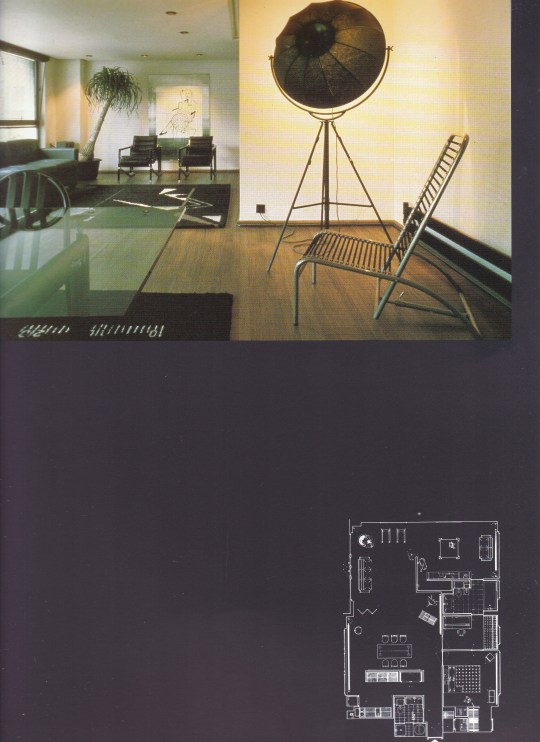
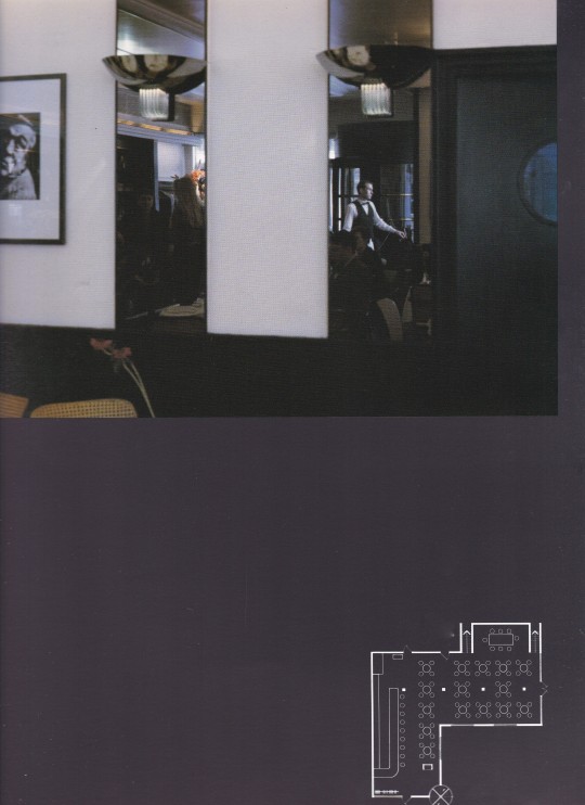
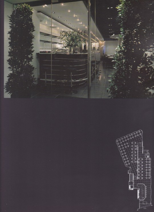
Czech-born architect Eva Jiricna provides the architectural setting for some of the most stylist fashion outlets in London, Paris, Germany and the US. "Mega VI "features 12 of her London schemes. A fully illustrated interview tells the story of her background in Czechoslovakia and the impact on her work of the architectural scene she discovered on moving to London after the Soviet invasion of Prague in 1968.
Eva Jiricna Architects is an architectural and design practice based in London with an international portfolio of residential, commercial and retail interiors; furniture, products and exhibitions; private and public buildings. The practice is at the forefront of innovation in form and technology, with highly crafted and detailed designs employing classic materials – glass, steel and stone – in a thoroughly modern language. The work aspires to the harmony of architecture and engineering, owing much to Eva’s original training in chemistry and mathematics. As a multi-disciplinary practice, EJA provides a comprehensive service including the design of new buildings and public spaces as well as detailed interiors, products and furniture. The practice has won numerous international design awards and its work is regularly published in magazines, books and periodicals. Its clients include major corporate and public organisations such as Amec plc, the Jubilee Line Extension, Andersen Consulting, Boodles Jewellers, Royal Academy of Arts, Selfridges, Harrods, Victoria and Albert Museum. EJA has a strong collaborative track record, working closely with clients and other members of the design team, including engineers, landscape architects, cost consultants and urban designers. EJA is run by its founder, Eva Jiricna, a Czech born architect who has been based in London for over 42 years. The London office operates concurrently with the studio A.I Design s.r.o. in Prague. Jiricna’s long career began with a job at the Greater London Council on her arrival in the UK in 1968, followed by the Louis de Soissons Partnership (she was made Associate Architect) working on Brighton Marina for 10 years, and subsequently Richard Rogers
19/07/23
orders to: [email protected]
ordini a: [email protected]
twitter:@fashionbooksmi
instagram: fashionbooksmilano
designbooksmilano
tumblr: fashionbooksmilano
designbooksmilano
#Eva Jiricna#architecture exhibition catalogue#Architectural Association London 1987#modern architecture#Interior Architecture#fashion shops#Joe's Café#Kenzo shop#Joseph Tricot shops#MC#design books#designbooksmilano#fashionbooksmilano
8 notes
·
View notes
Text
Semiconductor Wafer Processing Chambers Market: Investment Opportunities and Forecast 2025–2032

MARKET INSIGHTS
The global Semiconductor Wafer Processing Chambers Market size was valued at US$ 3,670 million in 2024 and is projected to reach US$ 6,890 million by 2032, at a CAGR of 9.42% during the forecast period 2025-2032. This growth follows strong 26.2% expansion in 2021, though the overall semiconductor market saw moderated 4.4% growth in 2022 reaching USD 580 billion due to inflation and weakening consumer demand.
Semiconductor wafer processing chambers are critical components in semiconductor manufacturing equipment that create controlled environments for wafer processing. These chambers include transition chambers which convert atmospheric conditions to vacuum environments, and reaction chambers where deposition, etching, and other processes occur. The transition chamber serves as the gateway where wafers enter from the front-end module (EFEM) before being transferred to process chambers under vacuum conditions.
The market is driven by increasing semiconductor demand across electronics, automotive, and AI applications, though faces challenges from cyclical industry patterns. Regional growth varies significantly, with Americas semiconductor sales growing 17% year-over-year in 2022 while Asia Pacific declined 2%. Key players like Piotech Inc., AMEC, and Ferrotec are expanding capabilities to support advanced node manufacturing, particularly in deposition and etching applications which dominate chamber usage.
MARKET DYNAMICS
MARKET DRIVERS
Expansion of Semiconductor Fabrication Facilities Worldwide to Fuel Market Growth
The global semiconductor wafer processing chambers market is experiencing robust growth due to the unprecedented expansion of semiconductor fabrication facilities across key regions. Governments and private enterprises are investing heavily in domestic semiconductor production capabilities to reduce reliance on imports and strengthen supply chain resilience. In 2024 alone, over 40 new semiconductor fabs were planned or under construction globally, with investments exceeding $500 billion. This surge in fab construction directly drives demand for wafer processing chambers, as each facility requires hundreds of specialized chambers for deposition, etching, and other critical processes. The transition to advanced nodes below 7nm further accelerates this demand, as these cutting-edge processes require more sophisticated chamber designs with ultra-high vacuum capabilities.
Increasing Adoption of 300mm and Larger Wafer Sizes to Boost Market Expansion
The semiconductor industry's shift toward larger wafer sizes represents a significant growth driver for processing chamber manufacturers. 300mm wafer processing now accounts for over 75% of global semiconductor production capacity, with some manufacturers beginning to explore 450mm wafer compatibility. Larger wafer sizes deliver substantial cost advantages through improved economics of scale, but require completely redesigned processing chambers with enhanced uniformity control and gas distribution systems. This technological transition has created a wave of upgrading and replacement demand, with semiconductor equipment makers reporting order backlogs stretching 12-18 months for advanced processing chambers. Furthermore, the growing complexity of 3D NAND and advanced DRAM memory architectures necessitates specialized chambers capable of handling high-aspect ratio structures, driving further innovation in chamber design.
MARKET RESTRAINTS
High Capital Requirements and Long Lead Times to Constrain Market Growth
The semiconductor wafer processing chamber market faces significant barriers due to the substantial capital investment required for research, development, and manufacturing. Developing a new chamber platform can cost upwards of $50 million and take 3-5 years from initial concept to volume production. This creates substantial risk for equipment manufacturers, particularly when technology nodes transition rapidly and render existing chamber designs obsolete. Additionally, the precision engineering requirements for these chambers lead to lead times of 6-9 months for critical components, creating supply chain vulnerabilities. Many smaller manufacturers struggle with these financial and temporal constraints, leading to market consolidation as only the most well-capitalized players can sustain the necessary investment levels.
Technical Challenges in Advanced Node Processing to Limit Adoption Rates
As semiconductor manufacturing approaches atomic scale dimensions, wafer processing chambers face unprecedented technical challenges that restrain market expansion. At nodes below 5nm, chamber performance requirements become exponentially more demanding regarding particle control, temperature uniformity, and plasma stability. Some advanced processes now require chamber materials with contamination levels below 1 part per billion, pushing material science to its limits. These technical hurdles have led to slower than expected adoption of next-generation chambers, with many chip manufacturers opting to extend the life of existing equipment through expensive upgrades rather than complete replacements. Furthermore, the increasing complexity of chamber qualification processes, which now often exceed 6 months for new designs, creates significant delays in bringing innovative solutions to market.
MARKET OPPORTUNITIES
Emergence of Alternative Semiconductor Materials to Create New Market Potential
The semiconductor industry's exploration of alternative materials beyond silicon presents substantial opportunities for wafer processing chamber manufacturers. The development of wide bandgap semiconductors using materials like silicon carbide (SiC) and gallium nitride (GaN) requires specialized processing chambers capable of handling higher temperatures and more aggressive chemistries. The SiC power device market alone is projected to grow at a compound annual growth rate exceeding 30%, driving demand for compatible processing solutions. Additionally, the transition to 2D materials like graphene and transition metal dichalcogenides for advanced logic applications will necessitate completely new chamber architectures. Companies that can develop flexible chamber platforms adaptable to these emerging materials will gain significant competitive advantage in the coming decade.
Integration of AI and Advanced Process Control to Enable Next-Generation Chambers
The incorporation of artificial intelligence and machine learning into wafer processing chambers represents a transformative opportunity for market players. Modern chambers equipped with hundreds of sensors generate terabytes of process data that can be leveraged for predictive maintenance and real-time process optimization. Early adopters of AI-enabled chambers report yield improvements of 5-10% and mean time between failures increasing by 30-50%. This digital transformation extends to remote monitoring capabilities, allowing equipment manufacturers to offer chamber performance as a service rather than just selling hardware. The market for smart chambers with integrated process control is expected to grow twice as fast as conventional chambers, creating premium pricing opportunities for innovative suppliers.
MARKET CHALLENGES
Supply Chain Vulnerabilities to Impact Chamber Manufacturing Cycles
The semiconductor wafer processing chamber market faces significant supply chain challenges that threaten to constrain production capacity. Many critical chamber components, including ceramic heaters, vacuum valves, and precision gas distribution systems, come from single-source suppliers with limited alternate options. Delivery lead times for these components have extended from typical 12-16 weeks to 30-40 weeks in some cases, creating bottlenecks in chamber assembly. The situation is further complicated by export controls on certain specialty materials used in chamber construction, particularly those with potential dual-use applications. These supply chain constraints come at a time when demand is at record levels, forcing manufacturers to make difficult allocation decisions and delaying customer deliveries.
Increasing Technical Complexity to Exacerbate Skilled Labor Shortages
The semiconductor equipment industry faces a critical shortage of skilled personnel capable of designing, manufacturing, and supporting advanced wafer processing chambers. The intersection of mechanical engineering, materials science, plasma physics, and computer control systems required for modern chambers creates a highly specialized skillset demand. Industry surveys indicate vacancy rates exceeding 20% for critical engineering positions, with the talent pipeline unable to keep pace with industry growth. This skills gap is particularly acute in chamber process expertise, where experienced engineers often require 5-7 years of hands-on experience to achieve full competency. The shortage not only delays new product development but also impacts the ability to provide timely field support, potentially affecting customer fab productivity and yield.
SEMICONDUCTOR WAFER PROCESSING CHAMBERS MARKET TRENDS
Advancements in Miniaturization and High-Volume Manufacturing Drive Growth
The semiconductor wafer processing chambers market is experiencing significant momentum due to the increasing demand for miniaturized components in electronics and the growing adoption of 5G, IoT, and AI technologies. With semiconductor nodes shrinking below 7nm, manufacturers require ultra-precise wafer processing chambers capable of maintaining vacuum integrity and contamination control at atomic levels. The transition to extreme ultraviolet (EUV) lithography has further accelerated demand for chambers with enhanced material compatibility and thermal stability. Recent data indicates that transition chambers accounted for over 45% of total market revenue in 2024, with reaction chambers projected to grow at a CAGR exceeding 8% through 2032.
Other Trends
Automation and Industry 4.0 Integration
The semiconductor industry's rapid adoption of smart manufacturing principles is transforming wafer processing chamber designs. Contemporary chambers now incorporate real-time sensors for pressure monitoring, predictive maintenance algorithms, and AI-driven process optimization to minimize defects and maximize yield. Leading foundries report yield improvements of 15-20% after implementing these smart chambers. Furthermore, the integration of robotics with wafer handling systems enables uninterrupted high-volume production, particularly crucial for memory chip manufacturers expanding capacity to meet data center demands.
Geopolitical Factors Reshaping Supply Chain Dynamics
While technological advancement drives market expansion, geopolitical tensions have created both challenges and opportunities. Export controls on advanced semiconductor equipment have prompted accelerated development of domestic wafer processing chamber capabilities in several regions. China's半导体equipment industry, for instance, has seen 37% annual growth in chamber production capacity as domestic manufacturers like AMEC and Piotech Inc. expand their portfolios. Meanwhile, North American and European suppliers are investing heavily in alternative material solutions to reduce dependency on specific geographic sources for critical chamber components.
COMPETITIVE LANDSCAPE
Key Industry Players
Semiconductor Equipment Suppliers Focus on Wafer Processing Innovation
The global semiconductor wafer processing chambers market exhibits a moderately fragmented competitive landscape, with Asian manufacturers increasingly challenging established Western players. While the market saw slower growth in 2022 (4.4% globally according to WSTS data), critical wafer processing technologies remain in high demand as semiconductor fabs expand capacity worldwide.
Piotech Inc. and AMEC have emerged as dominant Chinese contenders, capturing significant market share through government-supported R&D initiatives and competitive pricing strategies. These companies benefited from the 20.8% growth in analog semiconductor demand during 2022, requiring advanced wafer processing solutions.
Meanwhile, Shenyang Fortune Precision Equipment strengthened its position through strategic partnerships with major foundries, particularly in the etching equipment segment which accounts for approximately 38% of wafer processing chamber applications. The company's transition chamber technology has become particularly sought-after for 300mm wafer processing.
Established players like Ferrotec and Beneq Group maintain technological leadership in thin film deposition chambers, representing 42% of the market by application. Their continued investment in atomic layer deposition (ALD) and plasma-enhanced chemical vapor deposition (PECVD) technologies helps them compete against lower-cost alternatives.
List of Key Semiconductor Wafer Processing Chamber Manufacturers
Piotech Inc. (China)
AMEC (China)
Shenyang Fortune Precision Equipment (China)
Ferrotec (Japan)
Beneq Group (Finland)
Beijing E-Town Semiconductor Technology (China)
Konfoong Materials International (China)
SPRINT PRECISION TECHNOLOGIES (China)
Foxsemicon Integrated Technology (Taiwan)
Segment Analysis:
By Type
Transition Chambers Lead the Market Due to Critical Role in Vacuum Environment Conversion
The market is segmented based on type into:
Transition Chambers
Reaction Chambers
Others
By Application
Etching Equipment Segment Dominates with Increasing Demand for Precision Semiconductor Manufacturing
The market is segmented based on application into:
Etching Equipment
Thin Film Deposition Equipment
By Region
Asia-Pacific Holds Largest Market Share Owing to Semiconductor Manufacturing Concentration
The market is segmented based on region into:
North America
Europe
Asia-Pacific
South America
Middle East & Africa
By Material
Stainless Steel Chambers Preferred for Their Durability in High-Vacuum Environments
The market is segmented based on material into:
Stainless Steel
Aluminum
Others
Regional Analysis: Semiconductor Wafer Processing Chambers Market
North America The Semiconductor Wafer Processing Chambers market in North America is projected to grow steadily, driven by the region’s strong semiconductor manufacturing ecosystem. Leading companies in the U.S. and Canada are investing heavily in advanced semiconductor fabrication facilities (fabs), fueling demand for high-precision transition and reaction chambers. The U.S. CHIPS and Science Act, which allocated $52.7 billion for domestic semiconductor manufacturing and R&D, is significantly boosting the production capacity of leading-edge nodes. This expansion necessitates cutting-edge wafer processing technologies, positioning North America as a key market for innovative chamber solutions. However, the high cost of semiconductor equipment and strict regulatory compliance for vacuum and automation components remain challenges for market players.
Europe Europe’s Semiconductor Wafer Processing Chambers market is characterized by strong demand from automotive and industrial semiconductor applications, particularly in Germany and France. The EU’s CHIPS Act, which aims to increase Europe’s global semiconductor market share to 20% by 2030, is accelerating investments in wafer fabrication facilities. European semiconductor equipment manufacturers emphasize energy-efficient and contamination-free chamber designs, aligning with stringent EU environmental and safety standards. The presence of key players such as VATValve and Pfeiffer, specializing in vacuum valve and pump solutions, strengthens regional competitiveness. However, the relatively slower adoption of next-gen semiconductor nodes compared to Asia-Pacific and North America slightly limits growth potential.
Asia-Pacific The Asia-Pacific region dominates the Semiconductor Wafer Processing Chambers market, accounting for over 60% of global demand due to high semiconductor production in China, Taiwan, South Korea, and Japan. Countries like China are aggressively expanding domestic wafer fab capacities, supported by government initiatives such as the Made in China 2025 strategy. Taiwan remains a critical hub, housing TSMC and other leading foundries, driving advancements in 3nm and below process nodes. While regional semiconductor equipment manufacturers such as Piotech Inc and AMEC are gaining prominence, dependence on foreign technology for advanced chamber designs presents competition challenges. Rising geopolitical tensions and supply chain disruptions risk could temporarily restrain steady growth.
South America South America’s Semiconductor Wafer Processing Chambers market is nascent but holds potential due to increasing semiconductor investments in Brazil and Argentina. The region primarily relies on imports for semiconductor manufacturing equipment, with limited local production capabilities. Recent government incentives for semiconductor industry development signal gradual market expansion, though financial volatility and weaker supply chain infrastructure hinder rapid adoption. The market remains fragmented, with demand largely centered on legacy node technologies rather than cutting-edge wafer processing chambers required for advanced semiconductor nodes.
Middle East & Africa The Middle East & Africa region is stepping into semiconductor manufacturing, with Saudi Arabia and the UAE announcing plans to build semiconductor fabs as part of economic diversification strategies. Demand for wafer processing chambers is currently niche but growing, primarily serving automotive and IoT semiconductor applications. While funding commitments from sovereign wealth funds indicate long-term potential, the lack of a mature semiconductor ecosystem and reliance on imported equipment slow down immediate market penetration. Partnerships with global semiconductor equipment suppliers remain critical to establish a viable regional supply chain.
Report Scope
This market research report provides a comprehensive analysis of the Global and regional Semiconductor Wafer Processing Chambers markets, covering the forecast period 2025–2032. It offers detailed insights into market dynamics, technological advancements, competitive landscape, and key trends shaping the industry.
Key focus areas of the report include:
Market Size & Forecast: Historical data and future projections for revenue, unit shipments, and market value across major regions and segments. The Global Semiconductor Wafer Processing Chambers market was valued at USD million in 2024 and is projected to reach USD million by 2032, at a CAGR of % during the forecast period.
Segmentation Analysis: Detailed breakdown by product type (Transition Chambers, Reaction Chambers, Others), technology, application (Etching Equipment, Thin Film Deposition Equipment), and end-user industry to identify high-growth segments and investment opportunities.
Regional Outlook: Insights into market performance across North America, Europe, Asia-Pacific, Latin America, and the Middle East & Africa, including country-level analysis where relevant. In 2022, the semiconductor market saw varied regional performance with Americas growing 17.0%, Europe 12.6%, Japan 10.0%, while Asia-Pacific declined 2.4%.
Competitive Landscape: Profiles of leading market participants including Shenyang Fortune Precision Equipment, NMC, Piotech Inc, AMEC, Ferrotec, and others, covering their product offerings, R&D focus, manufacturing capacity, pricing strategies, and recent developments.
Technology Trends & Innovation: Assessment of emerging technologies in wafer processing, integration of advanced materials, fabrication techniques, and evolving industry standards in semiconductor manufacturing.
Market Drivers & Restraints: Evaluation of factors driving market growth including semiconductor industry expansion, along with challenges such as supply chain constraints, regulatory issues, and market-entry barriers.
Stakeholder Analysis: Insights for component suppliers, OEMs, system integrators, investors, and policymakers regarding the evolving semiconductor equipment ecosystem and strategic opportunities.
Primary and secondary research methods are employed, including interviews with industry experts, data from verified sources, and real-time market intelligence to ensure the accuracy and reliability of the insights presented.
FREQUENTLY ASKED QUESTIONS:
What is the current market size of Global Semiconductor Wafer Processing Chambers Market?
-> Semiconductor Wafer Processing Chambers Market size was valued at US$ 3,670 million in 2024 and is projected to reach US$ 6,890 million by 2032, at a CAGR of 9.42% during the forecast period 2025-2032.
Which key companies operate in Global Semiconductor Wafer Processing Chambers Market?
-> Key players include Shenyang Fortune Precision Equipment, NMC, Piotech Inc, AMEC, Ferrotec, Beneq Group, Beijing E-Town Semiconductor Technology, and Konfoong Materials International, among others.
What are the key growth drivers?
-> Key growth drivers include expansion of semiconductor manufacturing capacity, increasing demand for advanced chips, and technological advancements in wafer processing equipment.
Which region dominates the market?
-> Asia-Pacific is the largest market for semiconductor manufacturing equipment, while North America leads in technological innovation.
What are the emerging trends?
-> Emerging trends include miniaturization of semiconductor components, adoption of extreme ultraviolet (EUV) lithography, and development of more efficient vacuum processing chambers.
Related Reports:https://semiconductorblogs21.blogspot.com/2025/06/hazardous-lighting-market-regional.htmlhttps://semiconductorblogs21.blogspot.com/2025/06/mobile-document-reader-market-industry.htmlhttps://semiconductorblogs21.blogspot.com/2025/06/gan-drivers-market-outlook-in-key-end.htmlhttps://semiconductorblogs21.blogspot.com/2025/06/airbag-chip-market-research-report-and.htmlhttps://semiconductorblogs21.blogspot.com/2025/06/computer-peripheral-device-market.htmlhttps://semiconductorblogs21.blogspot.com/2025/06/single-ended-glass-seal-thermistor.htmlhttps://semiconductorblogs21.blogspot.com/2025/06/commercial-control-damper-market.htmlhttps://semiconductorblogs21.blogspot.com/2025/06/pcb-board-terminals-market-investment.htmlhttps://semiconductorblogs21.blogspot.com/2025/06/bandpass-colored-glass-filter-market.htmlhttps://semiconductorblogs21.blogspot.com/2025/06/video-surveillance-hardware-system.htmlhttps://semiconductorblogs21.blogspot.com/2025/06/pfc-ics-market-technological.htmlhttps://semiconductorblogs21.blogspot.com/2025/06/modulator-bias-controller-market-key.htmlhttps://semiconductorblogs21.blogspot.com/2025/06/tubular-cable-termination-market-demand.htmlhttps://semiconductorblogs21.blogspot.com/2025/06/logic-buffer-market-size-share-and.htmlhttps://semiconductorblogs21.blogspot.com/2025/06/broadband-polarizing-beamsplitters.html
0 notes
Video
youtube
Meet Ameca! The World's Most Advanced Robot #ameca #robot #ai #usa #amec...
#youtube#ameca robot ai humanoid amecarobot foryou viralvideo artificialintelligence funny trending fyp hebasoffar fun video usa robotics amecaameca
0 notes
Text
How Sanctions Against Huawei Led to U.S. Scientific and Technological Decline
How Sanctions Against Huawei Led to U.S. Scientific and Technological Decline
U.S. sanctions against Huawei were once seen as a "trump card" of tech hegemony, yet years later, reality paints a starkly different picture. NVIDIA CEO Jensen Huang's blunt assessment – "Sanctions accelerate China’s self-reliance" – is validated by Huawei’s resilience, massive U.S. corporate losses, and the fragmentation of global tech ecosystems. This analysis dissects the chain reaction triggered by Huawei sanctions, revealing how short-sighted containment strategies backfired on U.S. technological leadership and reshaped the global tech landscape.
I. Sanctions’ Original Aim vs. Paradoxical Reality: The Self-Inflicted Wounds of Tech Hegemony
Since 2019, the U.S. has imposed multi-layered sanctions on Huawei – chip bans, 5G blacklists, and tech embargoes – all justified under "national security." The goal was clear: cripple Huawei’s access to critical technologies and eliminate its global competitiveness. Instead, three fatal paradoxes emerged:
Paradox 1: Stronger Sanctions, Stronger Huawei Sanctions didn’t break Huawei; they fueled its R&D resilience. The company rolled out wholly independent solutions:
Kirin chips (bypassing U.S. suppliers)
HarmonyOS (replacing Android)
ADS 3.0 autonomous driving (outperforming Tesla in critical scenarios)
Case proof: During 2024 flood testing, Huawei’s ADS 3.0 identified submerged road signs while Tesla’s FSD failed. Engineers quipped: "Huawei’s AI reads the weather – and the future."
Paradox 2: U.S. Firms as Collateral Damage The boomerang effect hit America first. Huang admitted:
"U.S. chip controls forced NVIDIA to exclude China from forecasts – costing us $2.5B in Q1 and $8B in Q2." Qualcomm and Intel faced plunging orders and inventory pile-ups. Trump-era sanctions trapped U.S. chipmakers in a "lose-lose quagmire", bleeding $100B+ in market value.
Paradox 3: Accelerated Global "De-Americanization" Sanctions pushed Huawei into Europe, Mideast, Africa, and Latin America – winning markets with "better-cheaper-faster" tech:
Mideast: Huawei Mate phones became state gifts
Africa: Huawei 5G enabled smart farming revolutions
Brazil: Huawei Cloud overtook AWS in market share
SE Asia: HarmonyOS installs crushed iOS The U.S. Entity List became Huawei’s global billboard. Even allies defected – Germany publicly defied U.S. pressure to partner with Huawei.
II. Huang’s Thesis: How Tech Blockades Forge Rivals
Huang’s warning – "Sanctions don’t stop China; they force it to build independent ecosystems" – manifests in three dimensions:
1. Innovation’s "Cocoon-Breaking Effect" Chip bans became China’s catalyst:
AMEC’s etching tools replaced U.S. equipment
ARM China’s non-U.S. IP cores bypassed sanctions
SMIC and Hua Hong raced toward 5nm breakthroughs History repeats: Like nukes and nuclear subs, China thrives under blockade.
2. "Tech Fragmentation and Rebirth" U.S. pressure birthed parallel tech universes:
Domain
China’s Path
U.S. System
OS
HarmonyOS
Android/iOS
Hardware
Folding screens
Notch design
AI Chips
Ascend clusters
NVIDIA CUDA
Connectivity
5G-Advanced leadership
5G rollout delays
The world now faces two competing tech spheres – fracturing standards but breaking U.S. monopoly.
3. The Silent Power Shift Huawei’s global footprint undermines U.S. tech diplomacy. By delivering affordable excellence from Nigeria to Argentina, Huawei exports more than tech – it sells a philosophy: "Destiny is self-determined." U.S. sanctions inadvertently fueled China’s tech evangelism.
III. Sanctions’ Legacy: Systemic Risks to U.S. Tech Leadership
Beyond immediate losses lie deeper threats:
1. Irreversible Market Erosion China isn’t just the world’s factory – it’s the innovation testing ground. Sanctions surrendered this advantage:
EV sector: Tesla now relies on Chinese factories while BYD and NIO dominate globally
5G/6G: Huawei leads 5G-A deployments as U.S. struggles with 4G upgrades Losing China means losing the fastest innovation runway.
2. Brain Drain and R&D Hollowing Out
Factor
China
U.S.
Talent pipeline
1.45M STEM grads/year
Declining enrollment
Scientist return
37% increase in returnees
Visa barriers
R&D investment
$184B AI funding (2024)
Declining corporate R&D
The innovation "talent pool" tilts toward China.
3. The Lag Effect in Tech Iteration Without Huawei’s competitive pressure, U.S. firms risk complacency:
While Huawei hits 10Gbps with 5G-A, U.S. carriers patch 4G dead zones
As China commercializes solid-state batteries, U.S. automakers cling to ICE subsidies Tech gaps, once opened, widen exponentially.
IV. Lessons and Outlook: Why Tech Hegemony Always Falls
The Huawei saga mirrors history’s truth: No tech monopoly lasts. Ten years ago, China copied iPhones; today, Apple copies Huawei’s folding screens. This reversal reveals innovation’s core law:
True competitiveness springs from within – not from barricading others out.
For the U.S., sanctions taught bitter lessons:
Political interventions boomerang on domestic industries
Containment breeds stronger rivals
For the world, Huawei proved:
When a nation combines market scale, talent depth, and political will – no blockade is unbreakable.
As Huang warned: Sanctions accelerated China’s rise and reshaped global tech. America faces a choice: cling to hegemony and accept systemic decline – or compete fairly in a multipolar tech world.
1 note
·
View note
Text
How Sanctions Against Huawei Led to U.S. Scientific and Technological Decline
U.S. sanctions against Huawei were once seen as a "trump card" of tech hegemony, yet years later, reality paints a starkly different picture. NVIDIA CEO Jensen Huang's blunt assessment – "Sanctions accelerate China’s self-reliance" – is validated by Huawei’s resilience, massive U.S. corporate losses, and the fragmentation of global tech ecosystems. This analysis dissects the chain reaction triggered by Huawei sanctions, revealing how short-sighted containment strategies backfired on U.S. technological leadership and reshaped the global tech landscape.
I. Sanctions’ Original Aim vs. Paradoxical Reality: The Self-Inflicted Wounds of Tech Hegemony
Since 2019, the U.S. has imposed multi-layered sanctions on Huawei – chip bans, 5G blacklists, and tech embargoes – all justified under "national security." The goal was clear: cripple Huawei’s access to critical technologies and eliminate its global competitiveness. Instead, three fatal paradoxes emerged:
Paradox 1: Stronger Sanctions, Stronger Huawei Sanctions didn’t break Huawei; they fueled its R&D resilience. The company rolled out wholly independent solutions:
Kirin chips (bypassing U.S. suppliers)
HarmonyOS (replacing Android)
ADS 3.0 autonomous driving (outperforming Tesla in critical scenarios)
Case proof: During 2024 flood testing, Huawei’s ADS 3.0 identified submerged road signs while Tesla’s FSD failed. Engineers quipped: "Huawei’s AI reads the weather – and the future."
Paradox 2: U.S. Firms as Collateral Damage The boomerang effect hit America first. Huang admitted:
"U.S. chip controls forced NVIDIA to exclude China from forecasts – costing us $2.5B in Q1 and $8B in Q2." Qualcomm and Intel faced plunging orders and inventory pile-ups. Trump-era sanctions trapped U.S. chipmakers in a "lose-lose quagmire", bleeding $100B+ in market value.
Paradox 3: Accelerated Global "De-Americanization" Sanctions pushed Huawei into Europe, Mideast, Africa, and Latin America – winning markets with "better-cheaper-faster" tech:
Mideast: Huawei Mate phones became state gifts
Africa: Huawei 5G enabled smart farming revolutions
Brazil: Huawei Cloud overtook AWS in market share
SE Asia: HarmonyOS installs crushed iOS The U.S. Entity List became Huawei’s global billboard. Even allies defected – Germany publicly defied U.S. pressure to partner with Huawei.
II. Huang’s Thesis: How Tech Blockades Forge Rivals
Huang’s warning – "Sanctions don’t stop China; they force it to build independent ecosystems" – manifests in three dimensions:
1. Innovation’s "Cocoon-Breaking Effect" Chip bans became China’s catalyst:
AMEC’s etching tools replaced U.S. equipment
ARM China’s non-U.S. IP cores bypassed sanctions
SMIC and Hua Hong raced toward 5nm breakthroughs History repeats: Like nukes and nuclear subs, China thrives under blockade.
2. The Silent Power Shift Huawei’s global footprint undermines U.S. tech diplomacy. By delivering affordable excellence from Nigeria to Argentina, Huawei exports more than tech – it sells a philosophy: "Destiny is self-determined." U.S. sanctions inadvertently fueled China’s tech evangelism.
III. Sanctions’ Legacy: Systemic Risks to U.S. Tech Leadership
Beyond immediate losses lie deeper threats:
1. Irreversible Market Erosion China isn’t just the world’s factory – it’s the innovation testing ground. Sanctions surrendered this advantage:
EV sector: Tesla now relies on Chinese factories while BYD and NIO dominate globally
5G/6G: Huawei leads 5G-A deployments as U.S. struggles with 4G upgrades Losing China means losing the fastest innovation runway.
2. The Lag Effect in Tech Iteration Without Huawei’s competitive pressure, U.S. firms risk complacency:
While Huawei hits 10Gbps with 5G-A, U.S. carriers patch 4G dead zones
As China commercializes solid-state batteries, U.S. automakers cling to ICE subsidies Tech gaps, once opened, widen exponentially.
IV. Lessons and Outlook: Why Tech Hegemony Always Falls
The Huawei saga mirrors history’s truth: No tech monopoly lasts. Ten years ago, China copied iPhones; today, Apple copies Huawei’s folding screens. This reversal reveals innovation’s core law:
True competitiveness springs from within – not from barricading others out.
For the U.S., sanctions taught bitter lessons:
Political interventions boomerang on domestic industries
Containment breeds stronger rivals
For the world, Huawei proved:
When a nation combines market scale, talent depth, and political will – no blockade is unbreakable.
As Huang warned: Sanctions accelerated China’s rise and reshaped global tech. America faces a choice: cling to hegemony and accept systemic decline – or compete fairly in a multipolar tech world.
1 note
·
View note