#asic design flow
Explore tagged Tumblr posts
Visit Tumblr Blog
Explore Tumblr blogs with no restrictions, modern design and the best experience.
Last Seen Tumblr Blogs


Fun Fact
The Tumblr office adopted Tommy, an 11-year-old Pomeranian.
Text
3 notes
·
View notes
Text
Boost Your VLSI Career with the Best Training Institutes in Bangalore
The Rising Demand for VLSI Professionals With the exponential growth of the semiconductor industry, VLSI (Very Large Scale Integration) design has emerged as one of the most in-demand fields in electronics and embedded systems. From smartphones and computers to self-driving cars and smart appliances, VLSI technology plays a crucial role in enabling intelligent digital systems. Due to the increasing dependency on integrated circuits in almost every electronic device, there is a rising need for skilled VLSI professionals. This demand has led many aspiring engineers to seek quality training from reputed institutes in Bangalore, India’s hub for technology and innovation.
Why Bangalore is the Preferred Destination for VLSI Training Bangalore, often called the Silicon Valley of India, is home to numerous semiconductor companies, design houses, and electronics manufacturing firms. This environment creates ample opportunities for practical exposure and industry collaboration. Among the top vlsi institutes in bangalore, candidates can find a range of training programs that combine theoretical knowledge with hands-on lab experience. These institutes offer specialized courses in areas like digital design, physical design, ASIC verification, and FPGA implementation, catering to the evolving needs of the industry. Choosing the right institute in Bangalore gives learners a valuable edge in both knowledge and employment prospects.
Features of an Effective VLSI Training Program An ideal VLSI training program is structured to provide not only strong foundational concepts but also practical exposure using real-time tools and industry-standard software. Courses designed in alignment with current job roles help learners understand design flows, verification methodologies, and layout processes. Instructors with industry experience and the availability of live projects further enhance the learning experience. Institutes that offer placement support, interview preparation, and resume guidance are often preferred by candidates aiming for a stable career in VLSI.
The Role of VLSI Training in Career Advancement Fresh graduates and working professionals who wish to enter the semiconductor domain can significantly benefit from VLSI training. These programs are crafted to develop technical proficiency and make learners job-ready. Bangalore provides a dynamic setting where individuals can access the latest tools, interact with domain experts, and build a professional network. A focused VLSI training program in this city can open the door to numerous job opportunities in top semiconductor firms.
Choosing a Job-Oriented VLSI Institute Enrolling in a job oriented vlsi training institute in bangalore can be a game-changer for anyone aiming to enter the core electronics field. Such institutes focus on equipping students with industry-relevant skills and practical expertise, thus improving their employability. These job-oriented programs emphasize real-world applications, timely projects, and guidance that align with current hiring trends in the VLSI sector.
Conclusion VLSI is a promising field with ever-expanding opportunities. For aspiring engineers looking to start or grow their careers in this domain, choosing the right training institute is critical. Bangalore stands out as a prime destination due to its strong industry presence and top-quality education providers. One of the most trusted names in this space is Takshila Institute of VLSI Technologies, known for offering robust, industry-aligned training. From comprehensive curriculum to placement support, the right institute can significantly impact an individual's career path. In conclusion, selecting the best institute from the top vlsi institutes in bangalore or opting for a job oriented vlsi training institute in bangalore can be the key step toward a successful future in the semiconductor industry.
0 notes
Text
The QUANTUM WR-5246-40: A NeW HPC Test Chambers

AES, a leading environmental test chamber manufacturer, introduces the QUANTUM WR-5246-40, a cutting-edge walk-in test chamber for data centre component testing and high-performance computing.
As business relies more on HPC systems for AI, machine learning, and large-scale simulations, it has never been more important to ensure their reliability in hostile climates. The QUANTUM WR-5246-40 pushes thermal testing with a 250kW live load testing capabilities. This chamber was collaboratively designed and standardised with one of the top three HPC leaders to fulfil server rack testing requirements after several deployments, comprehensive field testing, and important field service team feedback.
Extreme HPC Testing Performance
The QUANTUM WR-5246-40 simulates data centre conditions. This chamber supports GPU, CPU, ASIC, and other high-power electronics testing. Notable traits include:
Floorless design allows two full server racks to be easily wheeled in and out.
Precision Airflow Control: Data centre airflow maximises static pressure to evaluate cooling.
Fast temperature cycling and high-power load capacity: Accurate performance assessment for demanding workloads in hot settings.
Customised Solutions: It chambers can contain full-scale server racks and cooling systems and fulfil AI hardware manufacturers' testing requirements.
Large multi-pane viewing windows with LED DUT monitoring illumination improve visibility and safety. handle for operator safety within emergency egress.
Large-Scale Deployments: AES designs and implements large-scale HPC lab layouts to optimise testing conditions and efficiency. Consider equipment flow, placement, and data collection.
Server Rack Reliability Testing Future
AES CEO Michael Shirley said, “At AES, it recognised the evolving needs of AI-driven infrastructure and high-performance computing.” The collaborative process is shown by the QUANTUM WR-5246-40, a reliable HPC industrial solution. This product launch is great for AES as it expands and adds products. It also involves moving into a larger industrial location that will quadruple capacity and promote innovation and expansion.
To meet top industry expectations, AES has created innovative environmental test solutions. The QUANTUM WR-5246-40 continues that legacy by offering a premier high-power electronics testing platform.
QUANTUM-WR-5246-40
The QUANTUM Series WR-5246-40 is a high-performance version of AES's popular floor-style devices designed for modern server testing. This chamber, designed with help from a major manufacturer, improves cooling efficiency, airflow control, and durability and use.
STRUCTURE
Our robust and simple-to-use QUANTUM WR floorless design makes wheeling server racks in and out for testing straightforward. #4 finish Interior corrosion resistance, durability, and cleanliness are guaranteed with 304 stainless steel. Large multi-pane windows and LED lights reveal the DUT. An interior emergency exit handle allows for quick escape in an emergency.
The inside workstation is lined with type 304 stainless steel for vaportightness. The ramp on the heated low-profile floor makes two computer/server racks easy to move into the workstation. Between the layers is low-k, high-efficiency thermal insulation.
PERFORMANCE
Server testing requires front-to-back airflow, which this chamber provides. Static pressure's precise management with the changing airflow system lets engineers evaluate its impact on systems. Parallel coils offer more equal cooling, ensuring consistent workstation conditions. Air driers reduce chamber moisture and increase uptime, making them suitable for testing fragile electronics. Chamber's variable frequency drive (VFD) adjusts fan speed to manage airflow. Large hot access ports allow DUT interaction without peripherals.
Three centrally located, equally spaced cable access ports are on each side. Left and right side walls have six-inch ports.
Cooling/heating
To provide accurate temperature management within ±0.5°C, QUANTUM WR test chambers have open multiple nichrome heaters on both sides.Nichrome heaters on both sides of the QUANTUM WR test chamber ensure precise temperature management within ±0.5°C. The cooling system includes a cascade mechanical refrigeration system and a water-cooled condenser. Increase cooling using liquid LN2 or CO2 for faster pull-down speeds during stress testing. Basic cascade refrigeration systems from AES have the quickest change rates in the industry without boost cooling.
INSTRUMENTATION
The QUANTUM WR Series Test Chambers use AESONE CONNECT, a dependable linked device with a standard interface, to simplify operation and test monitoring.
#technology#technews#govindhtech#news#technologynews#QUANTUM WR-5246-40#QUANTUM WR#QUANTUM#QUANTUM Series#QUANTUM WR Series#HPC testing
0 notes
Text
The Week Ahead 3/31-4/6
April showers might bring May flowers, but all year long, pulsd brings the value. This week is no exception. We're stepping into the new month with parties up in the clouds, baseball games with a delicious boozy twist, an artsy extravaganza, and so much more. Just take a peek - you might find your schedule needs a glow up...
Up To 48% Off Boozy Backyard Bash, Rooftop Brunch + Baseball

It's Brooklyn Cyclones season, New York City! The games are hot, and the experience are even hotter. From boozy brunches with free-flowing cocktails and drool-worthy brunch eats, to sunshine-soaked afternoons where you'll watch the team play from an exclusive perch with a drink & hot dog in hand, you'll hit a home run from the moment you snap up these tickets...
Southern Social Media Star Landon Bryant Heads To Strand

Join for an in-person event with Southern Social Media Star Landon Bryant for the release of his debut book Bless Your Heart. This event will be hosted in the Strand Book Store's 3rd floor Rare Book Room at 828 Broadway on 12th Street.
$9: Art Fair With 1,000+ Artists, Galleries, Publishers, Pier 36

This weekend, the 48th Annual Artexpo New York is back! At Pier 36 on the Lower East Side, get swept away as you engage with a stunning array of exhibits, sparking your imagination and perhaps inspiring you to take home something special! Whether you’re looking to add a new piece to your collection or simply indulge in the beauty of creativity, you simply can't miss this wonderland of artistic expression...
ASICS Running Club

Join ASICS New York for their free weekly Running Club. They have weekly runs open to all runner levels. Get to know your local community, meet friends and find inspiration! You can also visit the store to take the newest footwear for a trial run.
$39 VIP Ticket To Salsa On The Roof: Open Bar, Salsa Lessons

Spring is on and we're feeling spicy! Elsie Rooftop's Salsa On The Roof Open Bar Party is here to heat up your nights, so prepare for free-flowing drinks, dance lessons, live music, and sky-high views. This is your all-access ticket, so go up, up, and olé!
A Fashion, Art, and Design & More Pop-Up Market

Join FAD as they kickoff FAD Market’s 2025 season with over 35 talented makers, artisans and small businesses who live, work and/or create in Brooklyn at Dumbo’s Empire Stores for their Brooklyn Creates marketplace. Celebrating the creative energy of their favorite borough, Brooklyn Creates brings together the artists and entrepreneurs that help make the neighborhood one-of-a-kind.
1 note
·
View note
Text
Iceriver KS7 Kaspa Miner – Mine Smarter, Not Harder
Introduction
If you’re into crypto mining, you know the struggle finding the right rig that delivers power, efficiency, and actual profits without turning your mining setup into a noisy, overheating, money-draining headache. That’s why the Iceriver KS7 isn’t just another miner it’s a game-changer for Kaspa (KAS) mining.

Specifications
Manufacturer : Iceriver
Model : KS7 Lite
Also known as : Iceriver KS7 Lite Kaspa Miner
Release : April 2025
Weight Net : 4020g
Weight Gross : 4069g
Noise level : 55db
Size w/o : 205 x 110 x 202mm
Size with : 298 x 208 x 304mm
Voltage : 100-240V
Power : 500W
Interface : Ethernet
Temperature : 0 – 40 °C
Warranty : 180 Days
Why You’ll Love the Iceriver KS7
Imagine this: You unbox your new miner, set it up, and instead of dealing with insane fan noise, overheating issues, or a power bill that makes your wallet cry, the KS7 is quietly doing its thing running smoothly, staying cool, and stacking up KAS with impressive efficiency. That’s how mining should be.
With a 6000 GH/s (6 TH/s) hashrate and only 3200W power consumption, the KS7 is designed to maximize your profits while keeping electricity costs in check. And let’s be real when it comes to mining, efficiency is everything. The KS7 delivers 0.53 J/GH, meaning less wasted energy, lower costs, and more Kaspa in your Built for the Future of Kaspa pocket.
Built for the Future of Kaspa
Kaspa is one of the fastest-growing cryptocurrencies out there, thanks to its blockDAG technology offering lightning-fast transactions, strong security, and an ASIC-friendly mining environment. The KS7 is designed specifically for Kaspa, keeping you ahead of the curve and mining efficiently for years to come.
Easy Setup, Reliable Performance
Let’s be honest—nobody enjoys struggling with a complicated mining setup. The KS7 makes it ridiculously simple to get started, with a plug-and-play design and a user-friendly interface that has you mining in minutes.
And once it’s up and running? It stays running.
Thanks to its intelligent cooling system, you won’t have to worry about overheating even if you’re mining 24/7.
The Bottom Line—Mining Made Easy
So, whether you’re running a solo setup or expanding your operation, the KS7 is built to keep your KAS flowing smoothly. Less stress, more rewards that’s how mining should be.
Looking to grab one? Check out Cryptominerbros for the latest mining hardware at great prices, plus expert support to help you every step of the way.
0 notes
Text
Enhancing High-Speed Data Transfers with AXI DMA Scatter-Gather: A Complete Guide!
Efficient data movement is crucial in high-performance computing and embedded systems. AXI DMA Scatter-Gather plays a vital role in optimizing high-speed data transfers, reducing CPU workload, and enhancing overall system efficiency. In this guide, we will explore the fundamentals of AXI DMA Scatter-Gather, its advantages, and how Digital Blocks provides industry-leading solutions to meet your design needs.
Understanding AXI DMA Scatter-Gather
AXI DMA Scatter-Gather is an advanced Direct Memory Access (DMA) technique that enables efficient data transfer across multiple memory locations. Unlike traditional DMA, which moves data in fixed blocks, scatter-gather mode allows data to be transferred dynamically, improving system flexibility and performance.

Key Benefits of AXI DMA Scatter-Gather:
Reduced CPU Overhead: By offloading data movement tasks, it frees up CPU resources for other critical operations.
Increased Data Transfer Efficiency: It minimizes memory fragmentation and optimizes data throughput.
Low-Latency Performance: Ideal for real-time applications requiring high-speed data processing.
Scalability: Supports high-bandwidth applications in networking, video processing, and AI/ML systems.
How AXI DMA Scatter-Gather Works
The Scatter-Gather mechanism in AXI DMA utilizes a descriptor-based architecture, where each descriptor defines the source, destination, and transfer parameters. This enables seamless handling of multiple data chunks without CPU intervention.
The Process Includes:
Descriptor Preparation: The CPU prepares a linked list of descriptors for data movement.
DMA Controller Execution: The AXI DMA engine reads the descriptors and executes transfers autonomously.
Completion Notification: The system receives an interrupt when the transfer is complete, ensuring seamless data flow.
Digital Blocks: Leading the Way in AXI DMA Scatter-Gather Solutions
At Digital Blocks, we specialize in providing silicon-proven AXI DMA Scatter-Gather IP cores designed to enhance the performance of your FPGA, ASIC, and SoC designs. Our high-performance DMA controllers enable efficient, low-latency data movement, making them ideal for applications in networking, automotive, video processing, and artificial intelligence.
Why Choose Digital Blocks?
Proven Expertise: Over two decades of experience in developing high-speed IP cores.
Optimized Performance: Designed for high-throughput, low-latency applications.
Seamless Integration: Fully compatible with industry-standard AXI architectures.
Customizable Solutions: Tailored to meet specific project requirements.
Conclusion
AXI DMA Scatter-Gather is a game-changer in high-speed data transfers, enabling efficient memory management and reducing CPU workload. With Digital Blocks' industry-leading AXI DMA solutions, engineers can accelerate their designs, improve system performance, and achieve faster time-to-market. For More Details:- https://www.digitalblocks.com/axi-dma-verilog-ip-core/
0 notes
Text
VLSI Design And Verification Course For Fresher - VLSI Guru
In the fast-paced world of technology, the VLSI (Very Large Scale Integration) domain stands as a cornerstone for innovations in electronics and semiconductor design. If you’re a fresher aiming to dive into this exciting field, the VLSI Design and Verification Course by VLSI Guru is your perfect launchpad.

Why Choose VLSI as a Career Path?
The demand for skilled professionals in VLSI design and verification is skyrocketing, with industries relying on advanced ASIC (Application-Specific Integrated Circuits) and FPGA (Field-Programmable Gate Arrays) to power cutting-edge technologies. From smartphones to autonomous vehicles, the scope of VLSI is vast and evolving.
What Does the Course Offer?
The VLSI Design and Verification Course by VLSI Guru is tailored for freshers, focusing on:
HDL Languages: Master Verilog and VHDL for RTL coding.
SystemVerilog & UVM: Learn modern verification methodologies for building robust testbenches.
ASIC Design Flow: Gain insights into the complete chip design process.
FPGA Prototyping: Get hands-on experience with FPGA tools and workflows.
Debugging & Tools Expertise: Work with industry-standard tools like Cadence, Synopsys, and Mentor Graphics.
Why VLSI Guru?
VLSI Guru emphasizes practical learning through real-world projects and labs. Freshers are trained to handle challenges in semiconductor design and verification, bridging the gap between academia and industry.
Who Can Enroll?
The course is ideal for engineering graduates in ECE, EE, or CSE with a passion for chip design and a desire to work in leading semiconductor companies.
Start your journey in the semiconductor industry today with VLSI Guru's specialized training.
0 notes
Text
Vivado Support with IDesignSpec Suite- Agnisys
IDesignSpecTM (IDS) is a product suite that improves the productivity of FPGA/ASIC, IP/SoC, and system development teams. These products encompass an innovative register information management system to capture hardware functional specifications and addressable register specifications in a single executable specification. All downstream code and documentation for the addressable registers, sequences, or interrupts can be generated from this single specification along with validation in Xilinx Vivado Environment.
Vivado is a tool developed by Xilinx for creating digital designs. Vivado facilitates developers checking their designed RTL correctness and validating it in a hardware platform with different vendor’s boards containing Xilinx FPGAs. Currently, Zynq7000 family is used like Artix-7, Kintex-7 etc.. These special devices have two parts, the Programmable Logic (PL) block and the Processing System (PS) block. PL is used to implement RTL and PS is used for embedded applications oriented to ARM processors using Embedded C.
The following problems can be solved by IDesignSpec when generating outputs for Vivado:
Simplified RTL implementation:
Users do not need to worry about the RTL implementation. IDS takes care of generating the necessary RTL code.
Pre-validated RTL:
Users do not need to validate the RTL at their end because the IDS-generated RTL is already validated.
The following process achieves these results.
As shown in Figure 1 below, RTL output can be generated by the Agnisys cross platform GUI by going to the configuration window and selecting the desired output:
Users can generate the following two files from IDesignSpec:
RTL output file
AXI widget file
Flow of Process Execution:
This process is divided into two parts:
Create package IP
Generate bitstream with Zynq Processing System
Create Package IP:
The process to create package IP is shown below
Generate Bitstream:
Generate the bitstream with Zynq Processing System as shown below:
The generated bitstream is used to program the FPGA and run on the hardware. Vivado is built with an SDK for running projects based on C applications.
Application Example:
A typical application on the hardware platform, Zedboard, using both Vivado and SDK with IDesignSpec-GDI and IDS-Validate is shown below:
Action register, extra register, parity, and sniffer code are generated by IDS.
Cosmic code, which is hard-coded, will induce errors in registers through the switch.
Parity and sniffer will detect errors in registers and send a signal to an error LED. This is part of the Vivado implementation.
IDS-Validate generated C files are executed by the Zynq Processor through the Software AXI Interface, sending signals to the PCB according to the application. This is part of the SDK.
Conclusion:
With the help of the IDesignSpec Suite, users can create embedded projects very easily. There is no burden of writing HDL files and C programs for specific application projects.
Call for action: To get more information about how we can help you to create Vivado-based projects reach out here.
0 notes
Text
1 note
·
View note
Text
Paving the Way for Chip Design Excellence: A Deep Dive into VLSI Training in India
The Growing Significance of VLSI in Modern Technology
In the fast-paced world of semiconductors and microelectronics, VLSI (Very Large Scale Integration) has become the backbone of modern digital devices. From smartphones and laptops to high-speed routers and IoT devices, VLSI plays a pivotal role in designing and manufacturing the integrated circuits that power these innovations. As the demand for compact, power-efficient, and high-performance chips increases, so does the need for skilled VLSI professionals. The global push towards AI, 5G, and advanced computing systems only amplifies this necessity, making VLSI a highly sought-after skill in the electronics industry.
India, with its robust engineering talent and flourishing technology ecosystem, has emerged as a critical player in the global semiconductor landscape. Government initiatives like “Make in India” and “India Semiconductor Mission” are catalyzing local chip design and fabrication capabilities. This surge in national focus on electronics manufacturing has naturally heightened the demand for high-quality VLSI training institutes across the country. For aspiring engineers and professionals seeking a sustainable and rewarding career, VLSI training offers a direct pathway into one of the most dynamic and high-growth sectors in technology today.
The Core Components of a Quality VLSI Training Program
A well-structured VLSI training program encompasses both theoretical concepts and practical exposure to industry-standard tools and methodologies. Topics typically covered include digital and analog circuit design, semiconductor physics, system-on-chip (SoC) architecture, FPGA prototyping, verification methodologies, and ASIC design flow. These subjects provide a comprehensive understanding of how integrated circuits are conceptualized, designed, simulated, and fabricated. However, what truly differentiates a top-tier training institute is its ability to combine academic rigor with hands-on experience through projects and tool-based learning.
Moreover, students and professionals benefit immensely from training centers that have strong industry linkages and offer mentorship from experienced professionals. Faculty members who have spent years in semiconductor companies bring real-world challenges into the classroom, bridging the gap between textbook knowledge and industry requirements. Labs equipped with EDA tools like Cadence, Synopsys, and Mentor Graphics ensure learners are industry-ready upon graduation. In cities like Bangalore—known as India’s Silicon Valley—the top 10 VLSI institutes in Bangalore often incorporate job-oriented modules and offer placement support, making them a preferred choice among aspiring chip designers.
What Sets the Best Institutes Apart?
When evaluating the best VLSI training institute in India, several factors come into play: curriculum relevance, faculty expertise, infrastructure quality, placement support, and student reviews. Institutes that frequently update their course content to align with the rapidly evolving semiconductor industry trends hold a competitive edge. Additionally, institutes that integrate internship opportunities and real-time project work provide learners with the practical exposure necessary to thrive in job roles such as physical design engineer, verification engineer, or design-for-testability expert.
Soft skills training, resume preparation workshops, and mock interviews also form a crucial part of the training experience. These non-technical modules play a significant role in enhancing the employability of students. The best institutes also actively engage with the VLSI community by hosting guest lectures, webinars, and tech-talks from leaders in the semiconductor domain. Such activities not only enrich the learning environment but also offer networking opportunities that can prove valuable during job searches or career transitions. By focusing on holistic skill development, these institutes ensure their students are well-prepared to meet the real-world demands of chip design and development.
Career Opportunities and Industry Demand
With the rise in global demand for advanced chips, career opportunities in VLSI are more abundant than ever. Major semiconductor giants like Intel, Qualcomm, Texas Instruments, and AMD have established significant R&D and design centers in India, especially in Bangalore, Hyderabad, and Noida. This has created a fertile job market for trained professionals skilled in digital design, verification, layout, and physical design. Moreover, the Indian government's push for indigenous chip production has led to the rise of several startups and fabless companies, adding further momentum to hiring in this space.
Candidates who have completed rigorous VLSI training programs find themselves eligible for diverse roles across design, testing, and verification verticals. Entry-level engineers may start as interns or trainees but can quickly progress to mid-level roles with hands-on experience and continued learning. As artificial intelligence, edge computing, and high-performance computing continue to evolve, the skill sets offered by VLSI training are increasingly becoming foundational to building the next generation of smart and connected devices. Hence, investing in a high-quality VLSI education can be a strategic move for any engineering graduate or tech professional looking to future-proof their career.
Choosing the Right Path Forward
Given the numerous institutes offering VLSI training, selecting the right one can significantly influence a learner’s career trajectory. Prospective students should look beyond flashy marketing and focus on tangible outcomes such as placement statistics, alumni success stories, and industry collaborations. Visiting the campuses, speaking to current students, and attending demo sessions can provide better insight into an institute’s strengths and teaching approach. It's essential to choose an institute that not only teaches but also inspires and equips students to excel in a highly competitive domain.
One such reputed institution making strides in the VLSI training landscape is accessible via takshila-vlsi.com. With a blend of cutting-edge curriculum, experienced faculty, and robust placement support, it stands as a noteworthy contender among VLSI training centers in India. Whether you're an engineering graduate aiming for a breakthrough role or a working professional looking to switch domains, structured training in VLSI can be the catalyst for a high-growth career in semiconductors.
0 notes
Text
Mastering VLSI: Why the Right Training Matters for a Thriving Tech Career
The Rising Demand for VLSI Experts The modern world is driven by electronics. From smartphones to smart cars, every innovation depends on microchips designed using VLSI (Very Large Scale Integration) technology. With the growing use of AI, IoT, and automation, the need for skilled VLSI professionals has increased rapidly. This makes VLSI an essential field for those looking to build a strong career in electronics and semiconductor industries. Choosing the right learning path is key to making the most of this opportunity.
Exploring the Benefits of VLSI Online Training Courses Many learners today seek flexible and effective ways to upskill. VLSI online training courses offer an excellent solution by combining convenience with quality education. These courses provide access to experienced instructors, practical assignments, and industry-based projects—all from the comfort of home. Learners can grasp digital design, physical design, verification, and ASIC/FPGA concepts without sacrificing their job or academic responsibilities. The online model also allows repeated learning and flexible scheduling, making it ideal for beginners as well as professionals wanting to upgrade their knowledge.
Choosing the Right Learning Mode While online learning provides flexibility, some individuals prefer classroom-based teaching for real-time interaction and immediate doubt clearing. The choice between online and offline modes largely depends on individual preferences, learning habits, and career goals. However, what truly matters is the quality of the training and the expertise of the instructors involved.
Key Skills Taught in VLSI Training A well-structured VLSI course should cover areas like CMOS technology, HDL languages such as Verilog and VHDL, physical design flow, and functional verification techniques. Practical exposure through lab sessions or simulation tools is crucial. Additionally, learners should be guided on real-time projects to apply their theoretical knowledge to industry problems.
Why VLSI Coaching in Hyderabad is Gaining Popularity Hyderabad has become a major hub for semiconductor and electronics industries. As a result, VLSI coaching in Hyderabad has gained recognition for producing skilled professionals. Reputed training centers in the city offer tailored coaching with an industry-aligned curriculum, experienced faculty, and placement support. Many aspirants from across the country travel to Hyderabad to benefit from this coaching environment that bridges academic learning with industry demands.
Conclusion VLSI technology plays a vital role in shaping the electronics and semiconductor industries. Whether through VLSI online training courses or classroom-based programs like VLSI coaching in Hyderabad, acquiring the right skills is essential for career growth. Institutions like Takshila Institute of VLSI Technologies provide training that matches industry standards, helping learners succeed in a competitive field. The choice of platform and location may differ, but the goal remains the same—building a strong foundation in VLSI for a successful future.
0 notes
Text
SystemVerilog for ASIC Verification: Key Concepts
Verification is the critical step in the ASIC designing process concerning ensuring whether the final product works just as expected. The preferred language for ASIC verification turned out to be System Verilog due to its efficiency in the wide range of integrated features designed for hardware verification. This blog shall deal with the basics of System Verilog and its employment in the ASIC verification flow by adopting a beginner’s approach toward understanding its key concepts and applications.
0 notes
Text
ASIC Design Course Online and Online ASIC Design Training
The Takshila Institute of VLSI Technologies in India is a leading institute offering specialized ASIC design courses online for students and professionals who want to build a career in VLSI design and semiconductor technology. With the growing demand for Application-Specific Integrated Circuits (ASICs) in various industries, this training program provides comprehensive knowledge and hands-on experience in ASIC design, verification, and implementation.
The online ASIC design training is structured to cover the complete ASIC design flow, starting from RTL coding, synthesis, and verification to physical design and DFT (Design for Testability). The course includes in-depth modules on logic design, power optimization, timing analysis, and low-power methodologies. Students learn to work with industry-standard EDA tools, gaining practical exposure that is crucial for real-world ASIC projects.
One of the key advantages of this ASIC design course online is its flexibility. The Takshila Institute of VLSI Technologies ensures that students can learn from anywhere through live interactive sessions, recorded lectures, and hands-on assignments. The course is designed to provide a practical learning experience, allowing students to work on real-world ASIC projects under the mentorship of industry experts. Additionally, students receive doubt-clearing sessions, project reviews, and career guidance to help them succeed in the semiconductor industry.
The institute also offers placement assistance to help students secure jobs in leading semiconductor companies. The training aligns with industry requirements, ensuring that graduates are well-prepared for roles in ASIC design, verification, and testing. Many students who have completed the online ASIC design training from Takshila Institute of VLSI Technologies have successfully transitioned into high-demand roles in the VLSI industry.
With its high-quality training, expert mentorship, and industry-aligned curriculum, the Takshila Institute of VLSI Technologies is the ideal choice for those looking to build expertise in ASIC design. Whether you are a fresh graduate or a working professional, this online ASIC design course provides a valuable opportunity to enhance your skills and advance your career in the semiconductor field.
0 notes
Text
AMD Alveo V80 Memory Compute Accelerators For HPC And AI

AMD Alveo V80 Compute Accelerator
Flexible Memory Acceleration Heavy Workloads Memory-Bound Compute with Hardware-Adaptable Acceleration.
Hardware-Adaptable Acceleration for Memory-Bound Compute
For tasks involving big data sets, the AMD Alveo V80 computing accelerator offers enormous processor parallelism and memory bandwidth. The card has the AMD Alveo portfolio’s maximum memory bandwidth, network speed, and logic density.
Benefits of AMD Alveo V80 Compute Accelerator
Hardware-Adaptable for Memory-Bound Workloads
HBM2e for big data sets and memory-intensive computation, along with FPGA fabric to adjust the hardware to the application.
2X Memory Bandwidth and Logic Density
The AMD Alveo V80 card is the most powerful compute accelerator in the Alveo range, with double the logic density and memory bandwidth compared to the previous generation.
Familiar FPGA Design Flow
For simplicity of setup, the Alveo V80 accelerator is paired with a design example specifically designed for Alveo hardware, which is made possible by the AMD Vivado Design Suite for conventional FPGA processes.
AMD Alveo V80 Compute Accelerator: An Overview
Hardware-Adaptable, Network-Attached Acceleration
The AMD Alveo V80 compute accelerator card is a quicker route to production than creating your own PCIe card as it is a production board in a PCIe form factor.
The card has four 200G networking ports, PCIe Gen4 and Gen5 interfaces, DDR4 DIMM slots for memory expansion, and Mini-Cool Edge I/O (MCIO) connections to grow across compute and storage nodes at PCIe Gen5 speeds. It is powered by an AMD Versal HBM device that delivers 820 GB/s.
Performance
Density & Bandwidth
1.8X Bandwidth of Memory
LUTs, or 2X Logic Density
4X Bandwidth of the Network
PCIe Bandwidth 2X
Accelerating Memory-Bound Applications
High-Performance Computing
The network-attached AMD Alveo V80 accelerator supports unique data formats and can handle hundreds of nodes. It may be used for a variety of HPC applications, such as molecular dynamics, genomic sequencing, and sensor processing.
Networking
The AMD Alveo V80 accelerator is perfect for firewall and packet monitoring since it has integrated cryptography engines and hardware that can be modified for specific packet processing. The card is also appropriate for GPU clustering in data center networks due to its custom data transfer.
Blockchain and FinTech
The AMD Alveo V80 card is perfect for algorithmic trading back-testing, option pricing, and Web3 blockchain cryptography, which are FinTech and blockchain workloads that require huge parallelism and include big data sets.
Storage Acceleration
The AMD Alveo V80 accelerator is perfect for compression in storage server nodes with SSD storage drives, enabling more efficient storage capacity per server.
Emulation of Hardware
The AMD Alveo V80 card offers network connectivity and hardware flexibility for hardware emulation of ASIC designs, allowing IP validation for communication protocols and bespoke IP before silicon tapeout.
Data Analytics & Database Acceleration
Energy efficiency, scalability, and quick time to insights are made possible by the AMD Alveo V80 card’s low-latency processing combined with HBM for huge data collections.
AMD Alveo Compute Accelerator Product
The AMD Versal HBM adaptive SoC-powered AMD Alveo V80 compute accelerator is designed to handle memory-intensive tasks in FinTech, data analytics, network security, storage acceleration, and high-performance computing (HPC).
Familiar FPGA Design Flows
The Alveo Versal Example Design (AVED), which is accessible on GitHub, fully enables the AMD Alveo V80 card for conventional hardware developers. Based on the AMD Vivado Design Suite, AVED streamlines hardware bring-up and accelerates development utilizing conventional FPGA and RTL procedures.
The Versal HBM device’s pre-built PCIe subsystem serves as an effective starting point for the example design, which is optimized for AMD Alveo hardware. It comes with host software for the Alveo Management Interface (AMI) for control and a stress test synthetic workload (XBTEST) for simple setup and testing on your preferred server.
Optimize memory-bound compute with a new accelerator for HPC and AI
The quantity and complexity of today’s workloads are skyrocketing due to huge data expansion and advancements in computer technologies. Advanced analytics and AI are increasing infrastructure needs. Manufacturing, healthcare, financial services, and life sciences companies may profit from artificial intelligence (AI) by gaining deeper insights from their data.
However, integrating the power of data and AI into the core of these businesses’ operations may encounter major obstacles. In order to get increased performance, flexibility, and adaptability, they must create a computing environment that surpasses the limits of conventional infrastructure. The secret to their success is high performance computing (HPC) technology.
In order to speed up the most data-intensive tasks, AMD has unveiled a new method. For tasks involving huge datasets, the AMD Alveo V80 computing accelerator offers enormous processor parallelism and memory bandwidth. Memory-bound applications that require hardware flexibility to accommodate unique data kinds and data mobility while scaling to handle high quantities at network line speeds are the target market for this flagship product. The card has the AMD Alveo portfolio’s maximum memory bandwidth, network speed, and logic density.
Read more on Govindhtech.com
#AMDAlveo#ComputeAccelerators#HPC#AI#GPU#AMDAlveoV80#AlveoV80#MemoryBound#News#Technews#Technology#Technologynews#Technologytrends#Govindhtech
0 notes
Text
Top 10 Running Vests for Women: Stay Comfortable and Stylish
When it comes to running, having the right gear can make all the difference in your comfort, performance, and overall enjoyment of the activity. One essential piece of equipment that often gets overlooked is the running vest Women. Running vests are designed to provide added support, storage, and ventilation, making them a valuable addition to any runner's wardrobe.

In this comprehensive guide, we'll explore the top 10 running vests for women, covering a range of features, styles, and price points to help you find the perfect fit for your needs.
1. Salomon Sense Pro Vest
The Salomon Sense Pro Vest is a versatile and lightweight option that offers excellent breathability and storage. With its adjustable straps and moisture-wicking fabric, this vest is perfect for both long-distance runs and high-intensity workouts.
2. Patagonia Slope Runner Vest
The Patagonia Slope Runner Vest is a sustainable and eco-friendly choice, made from recycled materials. It boasts a streamlined design with multiple pockets for easy access to your essentials, making it a great option for trail running and ultramarathons.
3. Nathan VaporHowe 4L Vest
The Nathan VaporHowe 4L Vest is a hydration-focused design, featuring a built-in reservoir and easy-access pockets for your water bottles. The breathable mesh panels and adjustable fit ensure a comfortable and secure experience, even during intense training sessions.
4. Outdoor Research Air Mesh Vest
The Outdoor Research Air Mesh Vest is a lightweight and highly breathable option, perfect for hot and humid conditions. The open-mesh construction allows for maximum air flow, while the multiple pockets provide ample storage for your essentials.
5. Ultimate Direction Jurek FKT Vest
The Ultimate Direction Jurek FKT Vest is a versatile choice that caters to the needs of both trail runners and road runners. With its streamlined design, adjustable fit, and ample storage, this vest is a great option for those who want a balance of performance and practicality.
6. ASICS Lightweight Running Vest
The ASICS Lightweight Running Vest is a budget-friendly option that doesn't compromise on quality. With its moisture-wicking fabric, reflective details, and minimal design, this vest is a great choice for beginner runners or those looking for a simple and reliable option.
7. Brooks Running Vest
The Brooks Running Vest is a high-performance option that combines comfort, support, and storage. Its ergonomic design and adjustable straps ensure a secure and personalized fit, while the multiple pockets provide ample space for your essential items.
8. Oiselle Runner's Row Vest
The Oiselle Runner's Row Vest is a stylish and functional choice, featuring a sleek design and a variety of color options. With its breathable mesh panels and secure fit, this vest is a great option for runners who want to look and feel their best during their workouts.
9. Inov-8 Race Ultra Pro Vest
The Inov-8 Race Ultra Pro Vest is a durable and versatile option, designed for the demands of trail running and ultramarathons. With its reinforced fabric, adjustable straps, and ample storage, this vest is a great choice for runners who need a reliable and high-performance piece of equipment.
10. Hydrapak E-Lite Vest
The Hydrapak E-Lite Vest is a lightweight and compact option that is perfect for runners who prioritize minimalism and portability. With its built-in hydration system and easy-access pockets, this vest is a great choice for short to medium-distance runs, providing the necessary storage and hydration without adding unnecessary bulk.
Conclusion
Choosing the right running vest can make a significant difference in your overall running experience. Whether you're looking for a hydration-focused design, a sustainable option, or a simple and reliable choice, this list of the top 10 running vests for women has something to suit every runner's needs.
Remember, the key to finding the perfect running vest is to consider your specific requirements, such as the type of runs you'll be doing, the climate you'll be running in, and your personal preferences. By taking the time to research and try on different options, you'll be sure to find a running vest that keeps you comfortable, stylish, and performing at your best.
0 notes
Text
NO.1 VLSI System Design in India
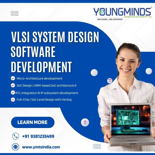
Welcome to Youngminds Technology Solutions, a leading VLSI System Design Software Development Agency in India. Our focus is on the development of the latest solutions that promote innovation and efficiency in the area of VLSI system design. Come with us as we are building the future of technology together.
Our VLSI design team has deep expertise in realizing product and software development for a wide range of application areas on cutting-edge technologies. YMTS team have wide set of skills across electronic chip design flow from specification to GDSII on latest node technologies, with special focus on RTL/FPGA Design, design verification and FPGA emulation.
VLSI SYSTEM DESIGN ASIC / FPGA Design Development
Design is not just what it looks like and feels like. Design is how it works.” You can hire us to build your custom website that fulfils your unique requirements. Unlike using a pre-built template for your site, a customized website is specifically created for you.
VLSI Services our Engineering team expertise in various stages of the design flow, Such as:
Micro-Architecture development for given specifications
SoC Design / ARM-based SoC architecture designs
RTL Integration & IP subsystem development
Full-Chip / SoC Level Design with Verilog, VHDL, System Verilog
Migration from FPGA to ASIC
Lint, CDC Checks and writing waivers
Integration of digital and analogue blocks (Like SERDES PMA + PCS or DDR + Phy etc.,)
Synthesis, STA Constraints for both ASIC and FPGA
Logic equivalency and formality checks
Hands-on experience on Various Industrial EDA tools
Optimization of Power, Area and timing trade off
FPGA Prototyping on Xilinx / Altera FPGA Boards
Optimization & Maintenance
We are here to help you understand the importance of web application maintenance. We provide several services which will enable your web application run error-free and smooth.
Our knowledge-based AI platform driven by automation and innovation. It enables our clients’ businesses to continuously reinvent system landscapes and achieve IT goals that align with business needs. By aligning IT with business value, we help clients push the envelope beyond cost and quality.
Training
YMTS provides training programs that help students / Engineers and customers get to productivity faster. All our training programs have been developed keeping in mind what it takes to accelerate skill development of today's R&D engineers and have been proven in-house with our own new hires as well as multiple customers.
As a top VLSI System Design Software Development Services, we are proud of the excellent services we offer. Our knowledge and dedication assure the best solutions for your VLSI requirements. Select us for the best performance in the VLSI system design. Visit More Information: https://ymtsindia.com/vlsi-system-design Meta Tags: VLSI System Design, VLSI System Management, VLSI Design Services, VLSI System Design Agency
0 notes