#compound semiconductor wafer supplier
Text
Epitaxial Wafer Market Trends Growth by Innovation in LED lighting
The epitaxial wafer market plays a pivotal role in manufacturing high-performance semiconductor devices used in applications ranging from consumer electronics to advanced healthcare devices. Epitaxial wafers aid in developing sophisticated integrated circuits and semiconductor chips through epitaxial growth techniques. Advancements in LED technology have increased the demand for epitaxial wafers for commercial and industrial applications. The global epitaxial wafer market is expected to gain significant traction on account of rising adoption of LED lighting and displays.
The Epitaxial Wafer Market size was valued at USD 2,778 million in 2022 and is anticipated to witness a compound annual growth rate (CAGR) of 12.9% from 2022 to 2030.
Key players operating in the epitaxial wafer market are EpiWorks Inc., Global Wafers Japan Co. Ltd., Nichia Corporation, SHOWA DENKO K.K., Siltronic AG, Desert Silicon Inc., Electronics and Materials Corporation Ltd. Intelligent Epitaxy Technology Inc.IQE plc., Jenoptic AG, MOSPEC Semiconductor Corporation, Norstel AB, Ommic S.A., Silicon Valley Microelectronics Inc., SVT Associates Inc. Universal Wafer Inc., Wafer Works Corporation, Xiamen Powerway Advanced Materials Co. Ltd., and Visual Photonics Epitaxy Co. Ltd.
Key Takeaways
Key players: EpiWorks, Global Wafers Japan, and Nichia captured over 35% share of the global market in 2024. EpiWorks leads the market with its diversified product portfolio and strong customer base.
Growing demand: Rising adoption of LED lighting, increasing penetration of advanced displays in consumer electronics and mobile devices, and growth of the semiconductor industry will continue to boost demand for epitaxial wafers in the coming years.
Global expansion: Leading manufacturers are investing heavily in capacity expansion plans across China, Taiwan, Europe, and the US to cater to the growing worldwide demand. Strategic partnerships and joint ventures are also gaining traction.
Market key trends
The Epitaxial Wafer Market Trends is undergoing significant transformation led by technological innovation in LED lighting applications. Manufacturers are focusing on developing high-quality mono-epitaxial and multi-epitaxial wafers to enable the mass production of more energy-efficient LED bulbs, streetlights, lamps, and advanced display backlights. Additionally, continuous ramp-up in wafer sizes from 150mm to 200mm and above is helping chipmakers lower production costs and improve epitaxial growth yield. This shift towards larger and more advanced epitaxial wafer substrates will define future market trends.
Porter’s Analysis
Threat of new entrants: New companies find it difficult to enter this market as a significant capital investment and technical expertise is required to set up manufacturing facilities for epitaxial wafers.
Bargaining power of buyers: Large technology companies like Intel, TSMC, Samsung, etc have significant bargaining power over epitaxial wafer suppliers given their high purchase volumes.
Bargaining power of suppliers: The presence of many established players limits the bargaining power of suppliers in this market.
Threat of new substitutes: There are limited substitutes for epitaxial wafers as they enable performance and cost benefits for several semiconductor devices.
Competitive rivalry: The market is dominated by few global players who compete intensely on technology leadership, quality, and customer service.
Geographical Regions
Asia Pacific accounts for the major share of the global epitaxial wafer market in terms of value owing to presence of large semiconductor manufacturing facilities and foundries located in countries like China, Taiwan, South Korea and Japan.
North America is expected to witness the fastest growth during the forecast period due to expanding semiconductor industry and ongoing technological advancements in the region. Rising demand for advanced semiconductor devices from sectors such as consumer electronics, automotive, industrial will drive the epitaxial wafer market in this region.
Get more insights on Epitaxial Wafer Market
About Author:
Money Singh is a seasoned content writer with over four years of experience in the market research sector. Her expertise spans various industries, including food and beverages, biotechnology, chemical and materials, defense and aerospace, consumer goods, etc. (https://www.linkedin.com/in/money-singh-590844163)

#Coherent Market Insights#Epitaxial Wafer Market#Epitaxial Wafer#Semiconductor Wafer#Epitaxy#Silicon Wafer#Semiconductor Materials#Epitaxial Layer#Microelectronics
0 notes
Text
The Photoresist Ancillaries Market is projected to witness substantial growth, with the market value expected to surge from USD 4,125.63 million in 2023 to reach USD 6,455.27 million by 2032, reflecting a notable compound annual growth rate (CAGR) of 5.10% during the forecast period.The photoresist ancillaries market plays a crucial role in the semiconductor and electronics industries, providing essential materials that support the manufacturing processes of integrated circuits (ICs), printed circuit boards (PCBs), and other electronic components. These ancillaries are integral to the photolithography process, which is foundational to creating intricate patterns on semiconductor wafers and other substrates.
Browse the full report at https://www.credenceresearch.com/report/photoresist-ancillaries-market
Market Overview
The global photoresist ancillaries market has witnessed steady growth in recent years, driven by advancements in semiconductor technology and the increasing demand for smaller, more efficient electronic devices. Photoresist ancillaries encompass a range of materials and chemicals, including developers, removers, primers, and edge-bead removers, among others. These materials are designed to enhance the performance and efficiency of photoresist materials used in photolithography processes.
Key Drivers of Market Growth
Several factors contribute to the growth of the photoresist ancillaries market:
1. Technological Advancements: Continuous innovations in semiconductor manufacturing technology, such as the development of advanced photoresists and ancillary materials, drive the demand for high-performance ancillary products.
2. Increasing Demand for Electronics: The proliferation of electronic devices across various sectors, including consumer electronics, automotive, and telecommunications, fuels the demand for advanced semiconductor components, thereby boosting the market for photoresist ancillaries.
3. Miniaturization Trends: The trend towards smaller and more complex electronic devices requires finer patterning capabilities, which in turn necessitates high-quality photoresist ancillaries for precise lithographic processes.
4. Geographical Expansion: Emerging economies in Asia-Pacific, particularly China, Japan, and South Korea, are significant contributors to market growth due to their expanding semiconductor and electronics manufacturing sectors.
Challenges and Opportunities
Despite robust growth prospects, the photoresist ancillaries market faces challenges such as stringent environmental regulations and volatility in raw material prices. Manufacturers are increasingly focusing on developing eco-friendly ancillary solutions and optimizing production processes to mitigate these challenges.
Opportunities abound for market players to capitalize on:
1. Research and Development: Investment in research and development to innovate new ancillary products that meet evolving technological requirements and regulatory standards.
2. Collaborations and Partnerships: Strategic collaborations between semiconductor manufacturers, research institutions, and ancillary suppliers can foster innovation and accelerate market penetration.
3. Market Expansion: Exploring untapped markets in emerging economies and diversifying product portfolios to cater to a wide range of applications in the electronics industry.
Future Outlook
The future of the photoresist ancillaries market looks promising with anticipated advancements in semiconductor technology and the growing adoption of advanced electronic devices worldwide. Continued investments in research and development, coupled with strategic initiatives to address environmental concerns, are expected to drive sustainable growth in the market.
Key Players
Tokyo Ohka Kogyo Co., Ltd.
JSR Corporation
Merck KGaA
Shin-Etsu Chemical Co., Ltd.
Dow Inc.
Fujifilm Holdings Corporation
MicroChem Corporation
Avantor, Inc.
DuPont de Nemours, Inc.
Sumitomo Chemical Co., Ltd.
Segments:
By Types:
Anti-reflective Coatings
Photoresist Developers
Edge Bead Removers
Other Type
By Application:
Semiconductors and Integrated Circuits
Printed Circuit Boards
Other Application
By Region
North America
Europe
Japan
Latin America
The Middle East and Africa
Asia-Pacific
About Us:
Credence Research is committed to employee well-being and productivity. Following the COVID-19 pandemic, we have implemented a permanent work-from-home policy for all employees.
Contact:
Credence Research
Please contact us at +91 6232 49 3207
Email: [email protected]
0 notes
Text
Semiconductor Sensors Market Analysis 2023 Dynamics, Players, Type, Applications, Trends, Regional Segmented, Outlook & Forecast till 2033
The semiconductor sensor market is expected to grow at a compound annual growth rate (CAGR) of 10.41% from 2024 to 2033, reaching a value of $319.6 billion by 2033. This is based on the 2023 market size of $201 billion.
The competitive analysis of the Semiconductor Sensors Market offers a comprehensive examination of key market players. It encompasses detailed company profiles, insights into revenue distribution, innovations within their product portfolios, regional market presence, strategic development plans, pricing strategies, identified target markets, and immediate future initiatives of industry leaders. This section serves as a valuable resource for readers to understand the driving forces behind competition and what strategies can set them apart in capturing new target markets.
Market projections and forecasts are underpinned by extensive primary research, further validated through precise secondary research specific to the Semiconductor Sensors Market. Our research analysts have dedicated substantial time and effort to curate essential industry insights from key industry participants, including Original Equipment Manufacturers (OEMs), top-tier suppliers, distributors, and relevant government entities.
Semiconductor Sensors Market Benefits
Semiconductor Sensors research reports provide critical insights for strategic decision-making. They help businesses understand market trends, customer preferences, and competitive landscapes. By analyzing data on market size, growth potential, and consumer behavior, companies can identify new opportunities and mitigate risks. These reports also guide product development, pricing strategies, and marketing campaigns, ensuring alignment with current market demands. Furthermore, market research reports enhance forecasting accuracy and help in benchmarking performance against competitors. Ultimately, they inform investment decisions, optimize resource allocation, and foster innovation, contributing to sustained business growth and a competitive edge.
Key Report Highlights:
Key Market Participants: The report delves into the major stakeholders in the market, encompassing market players, suppliers of raw materials and equipment, end-users, traders, distributors, and more.
Comprehensive Company Profiles: Detailed company profiles are provided, offering insights into various aspects including production capacity, pricing, revenue, costs, gross margin, sales volume, sales revenue, consumption patterns, growth rates, import-export dynamics, supply chains, future strategic plans, and technological advancements. This comprehensive analysis draws from a dataset spanning 12 years and includes forecasts.
Market Growth Drivers: The report extensively examines the factors contributing to market growth, with a specific focus on elucidating the diverse categories of end-users within the market.
Data Segmentation: The data and information are presented in a structured manner, allowing for easy access by market player, geographical region, product type, application, and more. Furthermore, the report can be tailored to accommodate specific research requirements.
SWOT Analysis: A SWOT analysis of the market is included, offering an insightful evaluation of its Strengths, Weaknesses, Opportunities, and Threats.
Expert Insights: Concluding the report, it features insights and opinions from industry experts, providing valuable perspectives on the market landscape.
Receive the FREE Sample Report of Semiconductor Sensors Market Research Insights @ https://stringentdatalytics.com/sample-request/semiconductor-sensors-market/9492/
Market Segmentations:
Global Semiconductor Sensors Market: By Company
• Figaro
• Honeywell
• Nissha
• Amphenol
• New Cosmos Electric
• Alphasense
• Sensorix
• MGK Sensor
• Shanghai AICI
• China Wafer Level CSP
• Zhengzhou Winsen
Global Semiconductor Sensors Market: By Type
• Temperature Sensor
• Pressure Sensor
• Humidity Sensor
• Gas Sensor
• Others
Global Semiconductor Sensors Market: By Application
• Industrial Automation
• Household Appliance
• Environmental Monitoring
• Medical
• Automobile
• Others
Regional Analysis of Global Semiconductor Sensors Market
All the regional segmentation has been studied based on recent and future trends, and the market is forecasted throughout the prediction period. The countries covered in the regional analysis of the Global Semiconductor Sensors market report are U.S., Canada, and Mexico in North America, Germany, France, U.K., Russia, Italy, Spain, Turkey, Netherlands, Switzerland, Belgium, and Rest of Europe in Europe, Singapore, Malaysia, Australia, Thailand, Indonesia, Philippines, China, Japan, India, South Korea, Rest of Asia-Pacific (APAC) in the Asia-Pacific (APAC), Saudi Arabia, U.A.E, South Africa, Egypt, Israel, Rest of Middle East and Africa (MEA) as a part of Middle East and Africa (MEA), and Argentina, Brazil, and Rest of South America as part of South America.
Click to Purchase Semiconductor Sensors Market Research Report @ https://stringentdatalytics.com/purchase/semiconductor-sensors-market/9492/
Report includes Competitor's Landscape:
➊ Major trends and growth projections by region and country
➋ Key winning strategies followed by the competitors
➌ Who are the key competitors in this industry?
➍ What shall be the potential of this industry over the forecast tenure?
➎ What are the factors propelling the demand for the Semiconductor Sensors?
➏ What are the opportunities that shall aid in significant proliferation of the market growth?
➐ What are the regional and country wise regulations that shall either hamper or boost the demand for Semiconductor Sensors?
➑ How has the covid-19 impacted the growth of the market?
➒ Has the supply chain disruption caused changes in the entire value chain?
Why to Purchase Semiconductor Sensors Market Report?
Purchasing a market research report provides valuable, reliable insights that are often beyond a company's in-house capabilities. These reports deliver comprehensive data on market trends, customer behaviors, competitive analysis, and industry forecasts, saving time and resources on extensive data collection and analysis. They offer expert perspectives and methodologies, ensuring credible, up-to-date information. By accessing tailored, actionable intelligence, businesses can make informed decisions, reduce uncertainty, and identify opportunities for growth. Additionally, these reports enhance strategic planning, risk management, and competitive positioning, making them a crucial investment for companies seeking to stay ahead in their industry and drive innovation.
Customization of the Report:
This report can be customized to meet the client’s requirements. Please connect with our sales team ([email protected] ), who will ensure that you get a report that suits your needs. You can also get in touch with our executives on +1 346 666 6655 to share your research requirements.
About Stringent Datalytics
Stringent Datalytics offers both custom and syndicated market research reports. Custom market research reports are tailored to a specific client's needs and requirements. These reports provide unique insights into a particular industry or market segment and can help businesses make informed decisions about their strategies and operations.
Syndicated market research reports, on the other hand, are pre-existing reports that are available for purchase by multiple clients. These reports are often produced on a regular basis, such as annually or quarterly, and cover a broad range of industries and market segments. Syndicated reports provide clients with insights into industry trends, market sizes, and competitive landscapes. By offering both custom and syndicated reports, Stringent Datalytics can provide clients with a range of market research solutions that can be customized to their specific needs.
Reach US
Stringent Datalytics
+1 346 666 6655
Social Channels:
Linkedin | Facebook | Twitter | YouTube
0 notes
Text
Diving into the World of Fuming Nitric Acid - Maruti Fine Chemicals
Today, we delve into the fascinating world of fuming nitric acid, commonly known as nitric acid fuming, and explore the wonders it holds. Today, we’ll discuss what fuming nitric acid is, its applications, and delve into the specifics of Nitric Acid 98% by Maruti Fine Chemicals. Let’s embark on this journey together!
What is Fuming Nitric Acid?
Fuming nitric acid is a highly concentrated form of nitric acid. It’s called “fuming” because it releases nitrogen dioxide gas, which gives off fumes when it comes in contact with air. This makes it different from regular nitric acid, which doesn’t release such fumes.
Uses of Fuming Nitric Acid
Fuming nitric acid has several important uses:
Chemical Synthesis: It’s used in the production of various chemicals, including explosives, dyes, and pharmaceuticals.
Etching: Fuming nitric acid is employed in the semiconductor industry for etching silicon wafers.
Nitrations: It’s used in the nitration of organic compounds, a process essential for making many products, including plastics and pharmaceuticals.
Nitric Acid 98% by Maruti Fine Chemicals:
Maruti Fine Chemicals is a reputable supplier of chemicals, including Nitric Acid 98%. This high-quality product is widely used in industries such as pharmaceuticals, textiles, and metallurgy. Here’s why Maruti Fine Chemicals’ Nitric Acid 98% stands out:

Q: Is fuming nitric acid dangerous to handle?
A: Yes, fuming nitric acid is highly corrosive and can cause severe burns upon contact with skin. Proper safety precautions, including wearing protective gear such as gloves and goggles, are essential when handling it.
Q: Can fuming nitric acid be stored safely?
A: Fuming nitric acid should be stored in a cool, dry place away from sources of heat and incompatible materials. It should be stored in properly labeled, tightly sealed containers to prevent exposure to air and moisture.
Q: What should I do in case of accidental exposure to fuming nitric acid?
A: In case of accidental exposure, immediately flush the affected area with plenty of water and seek medical attention promptly. It’s crucial to act quickly to minimize the risk of severe injury.
Q: Can fuming nitric acid be disposed of safely?
A: Proper disposal of fuming nitric acid is essential to prevent environmental contamination. It should be neutralized with an appropriate base, such as sodium bicarbonate, under controlled conditions, following all applicable regulations and guidelines.
Q: Is fuming nitric acid only used in industrial settings?
A: While fuming nitric acid is primarily used in industrial settings for various chemical processes, it also has niche applications in research laboratories and educational institutions for experimental purposes.
Conclusion:
In conclusion, fuming nitric acid is a potent chemical with diverse industrial applications. When handled with care and respect for its properties, it can be a valuable tool in various processes, contributing to advancements in technology and manufacturing. If you’re considering using fuming nitric acid, always prioritize safety and consult with experts for proper handling and disposal procedures. And if you’re in need of high-quality Nitric Acid 98%, consider Maruti Fine Chemicals for your supply needs.
0 notes
Text
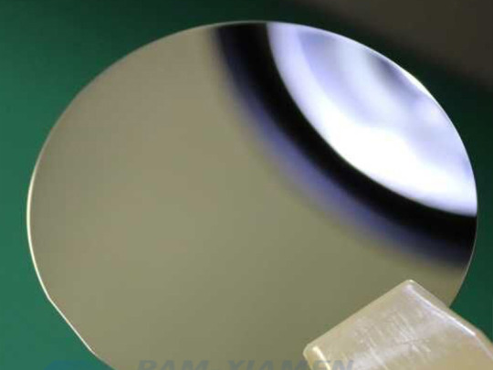
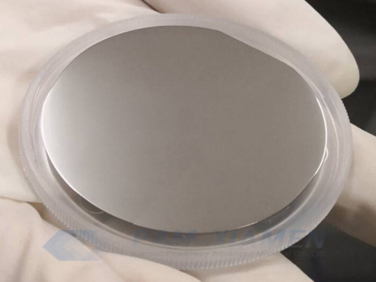
Wafers and Substrates
OST Photonics can supply lithium niobate (LiNbO3) wafers, lithium tantalate (LiTaO3) wafers, quartz single crystal wafers, various glass and fused silica wafers, GaAs wafers, SiC wafers, InP wafers, sapphire (Al2O3) wafers, Ge wafers and Si wafers in different specifications. Square plates, blanks and crystal boules are also available upon request. Other single crystal substrate materials including MgAl2O4, MgO, SrTiO3, LaAlO3, GGG, DyScO3, GdScO3, TbScO3, KTN, PMN-PT, LSAT, SrLaAlO4, YAG, YAlO3 (YAP) are also available on request.
What is the Difference Between SAW Grade Material and Optical Grade Material?
Optical grade materials are materials with low strain and no impurities, they are grown from the best raw materials at a relatively slow growth rate, and are often used in optical applications where the highest quality is required. Optical grade wafers are widely used in optical devices and require excellent optical performance.
SAW grade materials are primarily used in non-optical applications, and their growth raw materials rank second only to optical grade growth raw materials. The growth rate of this material is faster than that of optical grade material, which benefits mass production and cost-effectiveness.
In general, these grades of wafers vary in material quality and use. Optical grade wafers are considered to be of the highest quality, while SAW grade wafers are relatively lower in price. The selection of the appropriate wafer grade is crucial, depending on the specific application and material quality requirements.
FAQs of Wafers And Substrates
What is Epitaxy?
Epitaxial growth refers to the technique of growing crystalline layers with consistent crystal axes on a single crystal substrate, the epitaxial layer can be of the same material(Si/Si) or of different materials(SiGe/Si or SiC/Si).
What is the Pyroelectric Free Black LiNbO3/LiTaO3 Wafers?
We use a reduction technique to produce pyroelectric-free black LiNbO3/LiTaO3 wafers, which have a high ability to neutralize charges even if the electric potential occurs instantaneously. The pyroelectric effect of black LiNbO3/LiTaO3 wafers is almost eliminated and the transmittance is significantly reduced. The piezoelectric properties of black lithium niobate wafers are no different from those of standard wafers. Therefore, black-reduced lithium niobate wafers are widely used to produce higher-frequency surface acoustic wave devices.
What is the Difference Between Fused Silica and Quartz Single Crystal?
The key difference between fused silica and quartz single crystal is that fused silica contains non-crystalline silica glass whereas quartz contains crystalline silica. Fused silica is also known as fused quartz, it is a glass containing almost pure silica in an amorphous form. Quartz is a mineral compound containing silicon and oxygen atoms.
What is Single Crystal Substrate?
Single crystal substrate refers to the substrate materials used for epitaxial growth and the production of semiconductor devices.
What are Silicon Wafers Made?
Firstly, the silicon ore is purified to prepare polysilicon, and then the polysilicon is mixed with the dopant and melted for recrystallization to prepare a single crystal ingot. Finally, after ingot slicing, beveling, lapping, donor killing, polishing, cleaning, and other operations are performed to prepare silicon wafers with high flatness and surface cleanliness.
What is the Application of Silicon Wafer?
Silicon wafers are mainly used in various semiconductor chips, and then used in various electronic devices in daily life through various assembly, such as: TVs, computers, mobile phones, cars, etc.
What are the Advantages of Silicon as a Semiconductor Material?
1. The reserves of silicon on the earth reach 26.8%, second only to oxygen;
2. The energy gap of silicon is large (1.13V), which makes it have a higher operating temperature and lower leakage current;
3. The SiO2 layer on the surface of the silicon wafer can withstand high temperature and protect the silicon wafer.
What is the Relationship Between the Conductivity Type of the Silicon Wafer and the Dopant?
The dopants are mainly boron (B), phosphorus (P), arsenic (As), and antimony (Sb). Among them, the B-doped silicon wafer is P-type, which primarily conducts holes. The P-, As-, and Sb-doped silicon wafers are N-type and conduct electricity using electrons.

0 notes
Text
MIT, Applied Materials, and the Northeast Microelectronics Coalition Hub to bring 200mm advanced research capabilities to MIT.nano
New Post has been published on https://thedigitalinsider.com/mit-applied-materials-and-the-northeast-microelectronics-coalition-hub-to-bring-200mm-advanced-research-capabilities-to-mit-nano/
MIT, Applied Materials, and the Northeast Microelectronics Coalition Hub to bring 200mm advanced research capabilities to MIT.nano

The following is a joint announcement from MIT and Applied Materials, Inc.
MIT and Applied Materials, Inc., announced an agreement today that, together with a grant to MIT from the Northeast Microelectronics Coalition (NEMC) Hub, commits more than $40 million of estimated private and public investment to add advanced nano-fabrication equipment and capabilities to MIT.nano, the Institute’s center for nanoscale science and engineering. The collaboration will create a unique open-access site in the United States that supports research and development at industry-compatible scale using the same equipment found in high-volume production fabs to accelerate advances in silicon and compound semiconductors, power electronics, optical computing, analog devices, and other critical technologies.
The equipment and related funding and in-kind support provided by Applied Materials will significantly enhance MIT.nano’s existing capabilities to fabricate up to 200-millimeter (8-inch) wafers, a size essential to industry prototyping and production of semiconductors used in a broad range of markets including consumer electronics, automotive, industrial automation, clean energy, and more. Positioned to fill the gap between academic experimentation and commercialization, the equipment will help establish a bridge connecting early-stage innovation to industry pathways to the marketplace.
“A brilliant new concept for a chip won’t have impact in the world unless companies can make millions of copies of it. MIT.nano’s collaboration with Applied Materials will create a critical open-access capacity to help innovations travel from lab bench to industry foundries for manufacturing,” says Maria Zuber, MIT’s vice president for research and the E. A. Griswold Professor of Geophysics. “I am grateful to Applied Materials for its investment in this vision. The impact of the new toolset will ripple across MIT and throughout Massachusetts, the region, and the nation.”
Applied Materials is the world’s largest supplier of equipment for manufacturing semiconductors, displays, and other advanced electronics. The company will provide at MIT.nano several state-of-the-art process tools capable of supporting 150 and 200mm wafers and will enhance and upgrade an existing tool owned by MIT. In addition to assisting MIT.nano in the day-to-day operation and maintenance of the equipment, Applied engineers will develop new process capabilities that will benefit researchers and students from MIT and beyond.
“Chips are becoming increasingly complex, and there is tremendous need for continued advancements in 200mm devices, particularly compound semiconductors like silicon carbide and gallium nitride,” says Aninda Moitra, corporate vice president and general manager of Applied Materials’ ICAPS Business. “Applied is excited to team with MIT.nano to create a unique, open-access site in the U.S. where the chip ecosystem can collaborate to accelerate innovation. Our engagement with MIT expands Applied’s university innovation network and furthers our efforts to reduce the time and cost of commercializing new technologies while strengthening the pipeline of future semiconductor industry talent.”
The NEMC Hub, managed by the Massachusetts Technology Collaborative (MassTech), will allocate $7.7 million to enable the installation of the tools. The NEMC is the regional “hub” that connects and amplifies the capabilities of diverse organizations from across New England, plus New Jersey and New York. The U.S. Department of Defense (DoD) selected the NEMC Hub as one of eight Microelectronics Commons Hubs and awarded funding from the CHIPS and Science Act to accelerate the transition of critical microelectronics technologies from lab-to-fab, spur new jobs, expand workforce training opportunities, and invest in the region’s advanced manufacturing and technology sectors.
The Microelectronics Commons program is managed at the federal level by the Office of the Under Secretary of Defense for Research and Engineering and the Naval Surface Warfare Center, Crane Division, and facilitated through the National Security Technology Accelerator (NSTXL), which organizes the execution of the eight regional hubs located across the country. The announcement of the public sector support for the project was made at an event attended by leaders from the DoD and NSTXL during a site visit to meet with NEMC Hub members.
“The installation and operation of these tools at MIT.nano will have a direct impact on the members of the NEMC Hub, the Massachusetts and Northeast regional economy, and national security. This is what the CHIPS and Science Act is all about,” says Ben Linville-Engler, deputy director at the MassTech Collaborative and the interim director of the NEMC Hub. “This is an essential investment by the NEMC Hub to meet the mission of the Microelectronics Commons.”
MIT.nano is a 200,000 square-foot facility located in the heart of the MIT campus with pristine, class-100 cleanrooms capable of accepting these advanced tools. Its open-access model means that MIT.nano’s toolsets and laboratories are available not only to the campus, but also to early-stage R&D by researchers from other academic institutions, nonprofit organizations, government, and companies ranging from Fortune 500 multinationals to local startups. Vladimir Bulović, faculty director of MIT.nano, says he expects the new equipment to come online in early 2025.
“With vital funding for installation from NEMC and after a thorough and productive planning process with Applied Materials, MIT.nano is ready to install this toolset and integrate it into our expansive capabilities that serve over 1,100 researchers from academia, startups, and established companies,” says Bulović, who is also the Fariborz Maseeh Professor of Emerging Technologies in MIT’s Department of Electrical Engineering and Computer Science. “We’re eager to add these powerful new capabilities and excited for the new ideas, collaborations, and innovations that will follow.”
As part of its arrangement with MIT.nano, Applied Materials will join the MIT.nano Consortium, an industry program comprising 12 companies from different industries around the world. With the contributions of the company’s technical staff, Applied Materials will also have the opportunity to engage with MIT’s intellectual centers, including continued membership with the Microsystems Technology Laboratories.
#000#amp#analog#arrangement#Art#automation#automotive#bridge#Business#chips#clean energy#collaborate#Collaboration#collaborative#Companies#computer#computer chips#Computer Science#Computer science and technology#computing#consumer electronics#cybersecurity#defense#Department of Defense (DoD)#development#devices#displays#DOD#economy#Electrical Engineering&Computer Science (eecs)
0 notes
Text
Fan-out Wafer Level Packaging Market| Analysis and Forecast, 2023 – 2027
Originally published on Technavio: Fan-out Wafer Level Packaging Market by Technology, Type, and Geography - Forecast and Analysis 2023-2027
The Fan-out Wafer Level Packaging (FOWLP) Market is expected to experience significant growth from 2023 to 2027, driven by advancements in semiconductor packaging technologies, the demand for compact and high-performance electronic devices, and the increasing adoption of fan-out packaging solutions. The dynamics of this market are shaped by factors such as the technologies employed in FOWLP, the types of packages offered, and regional trends across the globe.
Fan-out wafer level packaging is an advanced semiconductor packaging technology that involves redistributing the traditional input/output (I/O) pads from the chip's perimeter to an area larger than the chip itself, creating a more space-efficient package. The market encompasses various technologies used in FOWLP, including mold-based fan-out (inFO) and laminate-based fan-out (lFo). inFO technology is known for its high-density packaging and reduced form factor, while lFo technology utilizes organic substrates, providing cost-effective and scalable solutions for semiconductor packaging.
The types of packages within the Fan-out Wafer Level Packaging Market include 2D fan-out packages and 3D fan-out packages. 2D fan-out packages involve redistributing the I/O pads in a two-dimensional plane, offering advantages in terms of size reduction and improved thermal performance. 3D fan-out packages, on the other hand, add an additional dimension by stacking multiple semiconductor dies vertically, providing enhanced performance and functionality in a compact form factor.
Geographically, the market is expected to showcase diverse trends, with North America, Europe, Asia-Pacific, and other regions significantly contributing to market growth. Asia-Pacific, particularly countries like China, Japan, and South Korea, is a key hub for semiconductor manufacturing, driving the demand for advanced packaging technologies such as FOWLP. North America and Europe also play pivotal roles in the market, with a focus on innovation in semiconductor packaging and the presence of leading semiconductor companies.
The forecast period is marked by ongoing innovations in FOWLP technologies, with a focus on improving integration capabilities, increasing the number of I/Os, and enhancing reliability. Manufacturers are exploring new materials, such as advanced mold compounds and organic substrates, to address thermal challenges and optimize the electrical performance of FOWLP solutions. Additionally, the market is witnessing efforts to expand the application scope of FOWLP to address the packaging needs of diverse semiconductor devices.
To Learn deeper into this report , View Sample PDF
Challenges in the Fan-out Wafer Level Packaging Market include addressing the complexity of high-volume manufacturing, ensuring compatibility with various semiconductor processes, and managing the cost considerations associated with advanced packaging technologies. However, the market's growth prospects remain positive as semiconductor manufacturers seek packaging solutions that offer higher integration, improved performance, and a smaller footprint. The industry's evolution is characterized by continuous research and development efforts, collaborations between semiconductor companies and packaging suppliers, and the integration of FOWLP into a broader range of applications, including mobile devices, automotive electronics, and Internet of Things (IoT) devices.
For more information please contact.
0 notes
Text
Ozone Generator Semiconductor
Ozone Generators: Mitigating Contamination Risks in Semiconductor Manufacturing
Semiconductor manufacturing processes require pristine environments to ensure optimal product quality. However, the presence of contaminants poses significant challenges.
Ozone functional gas systems have emerged as a valuable tool in mitigating contamination risks and maintaining the integrity of semiconductor manufacturing.

In this blog, we will explore the role of ozone generators and their benefits in this critical industry.
The Role of Ozone Generators
Ozone generators have become an effective contamination control solution in semiconductor manufacturing facilities.
Ozone (O3) is a highly reactive molecule that can neutralize and eliminate contaminants through oxidation.
Ozone's unique properties enable it to target and break down organic compounds, bacteria, viruses, and other microorganisms, minimizing the risk of contamination.
Benefits of Ozone Generators in Semiconductor Manufacturing
There are various benefits of using ozone gas generators in semiconductor manufacturing. Some of the popular ones are:
1. Enhanced Contamination Control:
Ozone generators provide enhanced contamination control in semiconductor manufacturing. By oxidizing and neutralizing contaminants, ozone effectively reduces the presence of airborne particles, volatile organic compounds (VOCs), and microorganisms.
It ensures a cleaner and more sterile environment within cleanrooms, minimizing the risk of contamination and improving product quality.
2. Improved Yield and Reliability:
The use of ozone generators in semiconductor manufacturing leads to improved yield rates and enhanced product reliability.
The risk of defective or faulty semiconductor devices is significantly reduced by eliminating or reducing the presence of contaminants, such as dust, organic compounds, or chemical residues.
These results in higher manufacturing success rates, increased productivity, and improved customer satisfaction.
3. Environmental Friendliness:
Ozone generators offer an environmentally friendly solution for contamination control. Ozone is a natural molecule that decomposes into oxygen (O2) after oxidation.
Unlike traditional chemical cleaning methods, ozone does not leave harmful residues or byproducts, minimizing the environmental impact of semiconductor manufacturing processes.
Implementing ozone generators aligns with sustainability goals and promotes a greener approach to semiconductor production.
4. Process Efficiency and Cost Savings:
Ozone generators contribute to process efficiency and cost savings in semiconductor manufacturing. They can be easily integrated into existing ventilation systems and operate continuously, requiring minimal maintenance. Ozone generators offer a reliable and automated contamination control solution, reducing manual labor and optimizing resource utilization. It leads to improved operational efficiency and cost-effectiveness in semiconductor manufacturing facilities.
5. Versatility and Multiple Applications:
Ozone generators have versatile applications beyond contamination control. They can be used for wafer cleaning, sterilization of equipment and tools, and disinfection of cleanrooms.
Ozone's ability to break down organic compounds and microorganisms makes it effective in a wide range of semiconductor manufacturing processes.
Its versatility allows semiconductor manufacturers to maximize the benefits of ozone generators across various applications, enhancing overall operational efficiency.
In summary:
youtube
Ozone generators play a crucial role in mitigating contamination risks in semiconductor manufacturing. Their ability to enhance contamination control, improve yield rates, ensure environmental friendliness, optimize process efficiency, and offer versatility makes them valuable in the industry.
If you are looking to purchase ozone generators for your semiconductor manufacturing facility, consider Inquivix Technologies as your trusted supplier. We offer a range of ozone generator semiconductor models tailored to the needs of specific industries, along with comprehensive customer support and service.
Contact us to learn more about ozone generators, or visit our website for a quote!
0 notes
Text
Quartz Sand: The Hidden Gem of Industrial Materials
Quartz sand, also known as silica sand, is composed of silicon dioxide (SiO2) and is one of the most abundant minerals found on the Earth's crust. It occurs in different forms, ranging from coarse to fine grains, and possesses excellent physical and chemical properties that make it a versatile material for numerous applications. Quartz sand is a versatile and widely used material in various industries. Its unique properties make it valuable in applications such as glass manufacturing, foundry molds, ceramics, water filtration, and more. To meet the growing demand for high-quality quartz sand, it is crucial to rely on a trusted supplier that can provide consistent and reliable products. Pratibha Refractory Minerals, a renowned company, has emerged as a reliable supplier of quartz sand, catering to the diverse needs of industries worldwide.

Applications of Quartz Sand in Different Industries
Quartz sand, also known as silica sand, finds extensive application in various industries due to its exceptional properties. Let's explore some of the key applications of quartz sand:
Glass Manufacturing: Quartz sand is a crucial component in the glass industry. It is used as the main raw material in the production of glass products such as bottles, windows, mirrors, and fiberglass.
Foundry and Casting: In the foundry industry, quartz sand is used in the casting process. It is mixed with binding agents to create molds and cores for metal casting.
Construction and Infrastructure: Quartz sand plays a significant role in the construction sector. It is used in the production of concrete, mortar, and asphalt mixtures. The fine particles of quartz sand fill in the gaps between larger aggregates, enhancing the strength, durability, and workability of construction materials.
Water Filtration: Quartz sand is an essential component of water filtration systems. Its high purity and porosity make it an excellent filter media for removing impurities and contaminants from water.
Ceramics and Refractories: Quartz sand is widely used in the ceramics and refractories industry. It is a key ingredient in the production of ceramic tiles, sanitaryware, porcelain, and refractory materials.
Oil and Gas Industry: Quartz sand is utilized in the oil and gas industry for hydraulic fracturing, or fracking. It is used as a proppant, a material that props open fractures in the rock formations, allowing the extraction of oil and gas.
Chemical Industry: Quartz sand finds applications in the chemical industry as a raw material for the production of various chemicals and compounds. It is used in the manufacturing of silicones, silicon wafers for the semiconductor industry, abrasives, catalysts, and other specialty chemicals.
Competitive Advantages of Pratibha Refractory Minerals
Pratibha Refractory Minerals, as a supplier of high-quality quartz sand, offers several competitive advantages that set them apart in the market. Let's explore some of these advantages:
High-Quality Products: We are committed to providing customers with high-quality quartz sand. They source their sand from reliable mines and employ stringent quality control measures at every stage of the supply chain.
Wide Range of Products: The company offers a diverse range of quartz sand products to cater to the specific needs of different industries. They provide various grain sizes and specifications, allowing customers to choose the most suitable sand for their applications.
Customized Solutions: We understand that each industry and application may have unique requirements. They work closely with customers to understand their needs and provide tailored solutions.
Customer Satisfaction: We place a strong emphasis on customer satisfaction. They prioritize understanding customer requirements, addressing their queries promptly, and providing efficient after-sales support.
Competitive Pricing: While offering high-quality products and exceptional service, Pratibha Refractory Minerals remains competitive in terms of pricing. They strive to provide cost-effective solutions without compromising on product quality or service standards.
Discover the secret to achieving impeccable results in your projects with Pratibha Refractory Minerals' superior Quartz Sand. As the leading supplier in the industry, we deliver the highest standards of quality, reliability, and performance, empowering you to unlock the full potential of your endeavors. Contact us today and let our premium quartz sand elevate your products to new heights!
0 notes
Text
Importance of Wafer Bonding in Today’s World
Wafer bonding is a phenomenon wherein at room temperature; mirror-polished, flat, and clean wafers of any material are brought in contact get attracted to each other by forces and adhere or bond. Wafer bonding is also known as direct bonding or fusion bonding. In maximum situations, the wafers that are included in actual applications are compound semiconductor wafers that consist of single-crystal materials such as silicon or gallium arsenide that are used in microelectronics or optoelectronics. When compared with that of covalently or ionically bonded solids the bonding at room temperature is usually weak. So for many applications, to strengthen the bonds across the interface the room-temperature-bonded wafers have to undergo heat treatment. Then one of the two wafers is thinned down to a thickness that may be in the range of many microns down to a couple of nanometers but depending on the specific application.
Today you will find that the most prominent applications of compound semiconductor wafer bonding are in the areas of silicon-on-insulator (SOI) devices and silicon-based sensors and actuators. SOI structures generally consist of a thin, top layer of single-crystal silicon, a layer of silicon dioxide (SiO2), and a silicon handle substrate that provides mechanical support. When the fabrication of SOI substrates is performed by wafer bonding, the silicon wafer that forms the top layer needs to be oxidized before bonding, and after bonding it needs to be thinned down to between 0.1 and 10 μm. When compared to devices on conventional silicon substrates, SOI devices that give hard radiation can operate at high temperatures and also have potentially higher packing density and lower power consumption.
Even after the dominance of silicon-related applications, wafer-bonding technology is by no means restricted to silicon wafers. Because of proper polishing and control of the chemistry of the surfaces, it has become possible to bond a variety of solids independently of their lattice parameter, structure (amorphous, polycrystalline, single-crystal), their crystallographic orientation, and or the thickness of the wafers. Hence, compound semiconductor wafer China bonding allows the fabrication of material combinations that were previously ruled out by most materials scientists, solid-state physicists, and electrical engineers, because by the conventional approach of epitaxial growth these material combinations were not possible.
Main source: https://ganwafer.wordpress.com/
#compound semiconductor wafer manufacturer#compound semiconductor wafer supplier#compound semiconductor substrate#compound semiconductor wafer china
3 notes
·
View notes
Text
Thin Wafer Market Share Size, Segments, Development, Opportunities, Forecast to 2029
Thin Wafer Market Summary 2022-2030
Straits Research's latest report on, Thin Wafer Market - Global Industry Overview and Forecast 2022-2030, highlights potential, risk factor Analyzes, and enhanced with strategic and tactical decision-making assistance. The growth and regulatory factors impacting information consumption, the availability of highly dependable items in the market, and the improvement in operating efficiency of Thin Wafer industry players. Thin Wafer Market Anticipated to Touch a CAGR of 5.9% During The Forecast Period 2017-2029 Thin Wafer Market Research covers market trends and development, drivers, capacities, technologies, and the changing dynamics of the Thin Wafer Market.
Competitive Landscape
Some of the prominent players operating in the Thin Wafer market are Industry Participants Key players in the global online hotel booking software market include GlobalWafers Co., Ltd, Shin-Etsu Chemical Co., My-Chip Production GmbH, EV Group, Siltronic AG, Polishing Corporation of America, Virginia Semiconductor Inc., ULVAC GmbH, Sil'tronix Silicon Technologies, Brewer Science, Inc., 3M Company, SK Siltron,among others.
Request a Sample Report for Free @ Thin Wafer Market Size 2022-2030
Studies explore the effects of COVID-19 on the upstream, midstream, and downstream sectors of the industry. In addition, this analysis provides extensive market estimations by putting an emphasis on data covering numerous factors that encompass market dynamics such as market drivers, market barriers, market opportunities, market risks, and industry news and trends.
This research also provides a dashboard view of prominent organizations highlighting their effective marketing tactics, market share and most recent advances in both historical and current settings.
Global Thin Wafer Market: Segmentation
As a result of the Thin Wafer market segmentation, the market is divided into sub-segments based on product type, application, as well as regional and country-level forecasts. By Wafer Size 125mm 200mm 300mm By Process Temporary Bonding and Debonding Carrier less/Taiko Process By Application MEMS CMOS Image Sensor Memory RF Devices LED Interposers Logic Others By Technology Wafer Grinding Wafer Polishing Wafer Dicing
The report forecasts revenue growth at all the geographic levels and provides an in-depth analysis of the latest industry trends and development patterns from 2020 to 2030 in each of the segments and sub-segments. Some of the major geographies included in the market are given below:
North America (U.S., Canada)
Europe (U.K., Germany, France, Italy)
Asia Pacific (China, India, Japan, Singapore, Malaysia)
Latin America (Brazil, Mexico)
Middle East & Africa
You may buy this document on Buy Thin Wafer Market Report
Tools and Insights:
A company's revenue and the applications market are used by market analysts, data analysts, and others in connected industries to assess product values and regional markets.
But not limited to: reports from corporations, international organizations and governments; market surveys; relevant industry news.
Examining historical market patterns, making predictions for the year 2022, as well as looking forward to 2030, using CAGRs (compound annual growth rates)
Historical and anticipated data on demand, application, pricing, and market share by country are all included in the study, which focuses on major markets such the United States, Europe, and China.
Apart from that, it sheds light on the primary market forces at work as well as the obstacles, opportunities, and threats that suppliers face. In addition, the worldwide market's leading players are profiled, together with their respective market shares.
Goals of the Study
Global Thin Wafer market consumption (value) by main areas and countries, product type (and application), statistics from 2019 to 2020 will be examined till forecast 2030.
Identify the different subsegments of the Thin Wafer market in order to better comprehend its structure.
Analysis of the value of the market, as well as the competitive landscape, Porter's five forces analysis and SWOT analysis of the top Thin Wafer worldwide manufacturers are included in this report.
We'll look at how well each of the Thin Wafer is doing and how much they contribute to market size.
Sharing in-depth information regarding the market's development factors (growth potential, opportunities, drivers, industry-specific challenges and risks).
According to main geographies, the consumption of Thin Wafer submarkets will be forecasted (along with their respective key countries).
To keep up with market changes, such as new product launches, expansions, and acquisitions.
To identify and assess the most important companies in the market, as well as their development plans.
The Table of Contents and Figures of the Full Report are available for your perusal Thin Wafer Market Report with TOC
Trending Report:
https://www.marketwatch.com/press-release/food-preservative-industry-to-expand-robustly-during-forecast-period-key-industry-players-cargill-incorporated-us-danisco-as-denmark-2022-06-14
https://www.marketwatch.com/press-release/high-pressure-relief-valves-industry-segmentation-by-top-market-players-leser-gmbh-cokg-emerson-electric-co-baker-hughes-2022-06-16
https://www.marketwatch.com/press-release/gluten-feed-industry-trends-by-forecast-2026-top-market-players-ingredion-incorporated-roquette-freres-archer-daniels-midland-company-2022-06-15
About Us:
StraitsResearch.com is a leading research and intelligence organization, specializing in research, analytics, and advisory services along with providing business insights & research reports.
Contact Us:
Email: [email protected]
Address: 825 3rd Avenue, New York, NY, USA, 10022
Tel: +1 6464807505, +44 203 318 2846
Website: https://straitsresearch.com/
0 notes
Text
Wafer-level Test and Burn-in [WLTBI] Market to Observe Strong Development by 2031
Transparency Market Research delivers key insights on the global wafer-level test and burn-in (WLTBI) market. In terms of revenue, the global wafer-level test and burn-in (WLTBI) market is estimated to expand at a CAGR of ~4% during the forecast period, owing to numerous factors, regarding which TMR offers thorough insights and forecasts in its report on the global wafer-level test and burn-in (WLTBI) market.
The global wafer-level test and burn-in (WLTBI) market is broadly affected by several factors, including high demand for usage of semiconductors in the automotive and telecom sectors. Thus, expanding applications of semiconductors in others industries is propelling the global market for wafer-level test and burn-in (WLTBI) for the test of semiconductor wafers.
Get PDF brochure for Industrial Insights and business Intelligence @ https://www.transparencymarketresearch.com/sample/sample.php...
Wafer-level Test and Burn-in (WLTBI) Market: Dynamics
Wafer-level test and burn-in is the process of subjecting semiconductor devices to electrical testing and burn-in, while the devices are still in wafer form. The burn-in is the temperature reliability stress test, which is used in detecting and screening out the potential early failures. Wafer-level test and burn-in is applicable to devices sold as a bare die, wafer level packaged devices, and devices that are intended for conventional packaging. In the last application, wafer-level test and burn-in is performed as a prescreen, so the parts that are passed can undergo backend processing. According to experts, the wafer level burn-in technology lowers the chip manufacturing costs by 15% and shortens the product lifecycle by 25%. The semiconductor industry has evolved significantly in the past 10 years, in terms of both technological advancements and changes to the industry’s value chain. As electronic gate sizes and other feature dimensions grow smaller and wafer sizes continue to increase, the cost of developing these technologies is also growing. Companies have to invest significantly more money in research and development each year in order to work on a competitive scale. These technological hurdles and the costs that accompany them have led to a restructuring of the industry value chain.
The advantages of the wafer-level test and burn-in process such as low cost, reliability, and simplicity have increased the attractiveness of wafer-level burn-in the market. In addition, the wafer-level and burn-in technology requires a single alignment step and a single dimensionally stable fixture to burn in hundreds of ICs simultaneously. This approach is much cheaper than using hundreds of precision die carriers. Additionally, other benefits include reduction in process steps when compared to packaged level and die level burn-in, reduction of wafer test insertion and probe time, and faster test result feedback to the fab. These benefits over other methods such as die level burn-in is fueling the market growth. Semiconductors are increasingly used in electronic systems and parts of automobiles such as infotainment, engine control, and safety features. Compound semiconductors, which are used in autonomous and self-driving cars require 100% burn-in due to natural material properties.
Key players in the wafer-level test and burn-in (WLTBI) market are already engaged in the development and introduction of advanced test solutions for semiconductor wafers. For instance, Aehr Test Systems’ wafer parks with FOX-XP multi-wafer test and burn-in systems have been in production and qualified by automotive suppliers for full wafer test of silicon carbide power devices since 2020. They are used in electric and hybrid electric vehicle power trains. Thus, introduction and development of advanced products in the wafer-level test and burn-in (WLTBI) market is expected to accelerate the implementation of new products. This is further expected to have a positive impact on the adoption of wafer-level test and burn-in (WLTBI) during the forecast period.
Purchase our Premium Research Report at: https://www.transparencymarketresearch.com/checkout.php?rep_id=82208<ype=S
Wafer-level Test and Burn-in (WLTBI) Market: Prominent Regions
The wafer-level test and burn-in (WLTBI) market in Asia Pacific is expected to expand during the forecast period, owing to the presence of key market players, technological advancements, and growth of semiconductor industries in the region. The wafer-level test and burn-in (WLTBI) market in Asia Pacific is projected to witness favorable growth during the forecast period, as many wafer foundry companies are located in APAC countries such as Taiwan, South Korea, Japan, and China. Moreover, many successful companies have chosen to outsource the fabrication of their hardware to dedicated manufacturing firms. These companies are often located in countries with lower labor costs, in which local fabricators have built up considerable experience and expertise in this form of specialized manufacturing. Furthermore, the rising adoption of advanced semiconductor components in developing economies in Asia Pacific, led by technological advancements and cost efficiency is projected to drive the market in the region during the forecast period, owing to which the market is projected to reach US$ 3.2 Bn by 2031. The wafer-level test and burn-in (WLTBI) market in Asia Pacific is likely to expand at the highest CAGR of 4.97% during the forecast period, due to the presence of a large number of players manufacturing wafer-level test and burn-in (WLTBI) in the region.
Wafer-level Test and Burn-in (WLTBI) Market: Key Players
Key players operating in the global wafer-level test and burn-in (WLTBI) market are Aehr Test Systems, Delta V Instruments Inc., Amkor Technology, Robson Technologies, Inc., Teradyne Inc., Abrel Products Ltd, Electron Test Equipment Limited, Pentamaster, and Advantest Corporation.
Global Wafer-level Test and Burn-in (WLTBI) Market: Segmentation
Wafer-level Test and Burn-in (WLTBI) Market, by Type
Single Wafer
Multi and Full Wafer
Wafer-level Test and Burn-in (WLTBI) Market, by Application
IDMs
OSAT
TMR Latest News Publication: https://www.prnewswire.com/news-releases/livestock-monitorin...
0 notes
Text
Gallium Arsenide (GaAs) Market Size Forecast to Reach $632.2 Billion by 2026
Gallium Arsenide (GaAs) Market Size is forecast to reach $632.2 billion by 2026, growing at a CAGR of 7.1% during 2021-2026. GaAs is increasingly used as a replacement for silicon because of its enhanced electronic properties and was selectively grown on GaAs substrates patterned with SiO2 by conventional molecular beam epitaxy. Moreover growing demand for GaAs across various end-user industries such as aerospace & defense, electronics, and communications is analyzed to drive the Gallium Arsenide Market share. In addition, owing to a wide direct band gap material that resists radiation damage, GaAs is an excellent option for outer space electronics and optical windows in high power applications. Further, other key factors driving the growth of the GaAs market include increase in adoption of 5G networks across the world and the advent of IoT has been one of the major reasons responsible for the growing trend of the Gallium Arsenide market size. The technology has given rise to a demand for high-frequency communication devices made with GaAs based ICs. Furthermore, this remarkable growth in the Gallium Arsenide market is providing a huge number of opportunities for wafer, EPI wafer & metal-organic chemical vapor deposition equipment suppliers, and manufacturers in the forecast period 2021-2026.
Request for Sample Report @ https://www.industryarc.com/pdfdownload.php?id=509501
Report Price: $ 5900 (Single User License)
Gallium Arsenide Market Segment Analysis - By Type
Vertical Gradient Freeze (VGF) Grown GaAs segment held significant market share of 40.5% in 2020. VGF Grown GaAs will remain the largest manufacturing technology, and it is expected to witness highest growth during the forecast period as it produces substrates with relatively low defect densities and higher mechanical strength. Vertical gradient freeze (VGF) technology is a proven technique for growing semiconductors composed of multiple elements that include gallium, arsenic, indium, and phosphorus. Such semiconductors offer capabilities that exceed those of wafers created on a single crystal silicon substrate. The main advantages of the VGF process include its scalability, low stress, high mechanical strength, and a defect rate that is orders of magnitude lower than conventional compound semiconductor crystal growth processes. Hence these benefits are analysed to drive the growth rate of the gallium arsenide market in the forecast period 2021-2026.
Gallium Arsenide Market Segment Analysis - By Application
Smart phones segment in Gallium Arsenide market is expected to witness a highest CAGR of 8.5% the forecast period. The demand for Gallium Arsenide is driven by smartphones and other applications across the consumer electronics industry, which require semiconductor ICs. In addition, increasing numbers of Internet of Things (IoT) devices is expected to force the semiconductor industry to invest in this equipment, in a bid to attain intelligent products. Moreover, the continuous advancements in consumer electronics and the use of sensors in various electronic products are proliferating the applications of plasma etching in smartphones and their demand across almost all the industry sectors. In 2018, the South Korean government announced to invest $1.34 billion for the next ten years to support the development of next-generation semiconductor technology, to support Samsung Electronics and SK Hynix. The investment will help Korean companies, such as Samsung and SK Hynix, to enhance their semiconductor manufacturing capabilities. Further with the powerful 5G cellular network being introduced to the world in 2019, mobile devices need a semiconductor that can handle the faster signal speed. As Gallium Arsenide will outperform silicon wafers due to its ultra-high frequency applications will enhance the demand for Gallium Arsenide industry in the forecast period 2021-2026.
Gallium Arsenide Market Segment Analysis - By Geography
Gallium Arsenide market in Asia-Pacific region held significant market share of 36.5% in 2020, owing to growing consumption of smartphones and other high-performance electronics devices in the region. Countries such as India, China, Taiwan, South Korea and so on are few of the prominent markets for Gallium Arsenide, and this is primarily attributed to the growing demand for advanced technologies across numerous end-user industries, high growth of the consumer electronics industry, rising support for the semiconductor industry in the region. In May 2019, Taiwan Semiconductor has opened new branch in Beijing to accommodate the rapid growth in China and engage local talent in its business development efforts. Moreover, the emergence of new technologies in Asia-Pacific has boosted the demand for innovative and user-friendly smart devices. There has been a rising demand from South Korea and Taiwan for semiconductor wafers, due to the large production of consumer electronic devices such as televisions, smartphones, PCs and so on. Further governments of several countries in this region are supporting the growth of semiconductor production by various initiatives, for instance, Made in Chine 2025, Make in India and others will promote the growth of semiconductor industries thereby increasing the growth of Gallium Arsenide market in the forecast period 2021-2026.
Inquiry Before Buying @ https://www.industryarc.com/reports/request-quote?id=509501
Gallium Arsenide Market Drivers
Growing Penetration of 5G
With the powerful 5G cellular network being introduced to the world in 2019, mobile devices need a semiconductor that can handle the faster signal speed. Gallium Arsenide due to its ultra-high frequency applications able to outperform silicon wafers in some of the most important ways. Moreover, with the emergence of 5G, silicon usage in semiconductors will be further reduced. Further for the implementation of 5G network, GaAs can be seen as the next generation of integrated circuits due to its high band gap, which drastically outperforms silicon. According to semiconductor Association, it is expected that the overall market for semiconductors could pass a whopping $20 trillion by 2025. This will create significant demand for GaAs in the forecast period. Furthermore governments of several countries have been investing heavily for the deployment of 5G. In 2019, China is expected to invest over $150 billion in its 5G networks through 2025. Similarly, Germany made a step towards accelerating the development of 5G services in the country, pouring additional investments into backing domestic endeavours. Hence growing penetration of 5g will drive the Gallium Arsenide Market growth in the forecast period 2021-2026.
Growth of Semiconductor industry creates significant demand for Gallium Arsenide Market
Growth of semiconductor manufacturing is analysed to create significant opportunities in the forecast period. In 2020, Indian Government is planning to offer around $1 billion in cash to every company that sets up a chip manufacturing unit in India. Similarly, China’s ‘Made in China 2025’ initiative will also create significant demand for semiconductor manufacturing in the forecast period. Moreover, U.S government is also committed to invest around $50 billion for the growth of semiconductor industry. Silicon is the most important material for semiconductor electronics. Silicon devices and integrated circuits are dominant in most applications from consumer electronics to automotive. However, in certain areas, silicon is being challenged by other semiconductor materials, such as gallium arsenide. Gallium arsenide excels in ultra-high frequency applications and has emerged as leading contenders for ultrahigh speed applications in the next generation of supercomputers and communication equipment. Hence Gallium arsenide has become relatively important and is expected to increase sharply in the forecast period 2021-2026.
Gallium Arsenide Market Challenges
High Production Cost
Although Gallium Arsenide market is growing at a significant phase it poses some difficulties, compared with that of silicon. For instance, unlike silicon, there is no natural oxide that acts as a mask to produce simple elements of the Complementary Metal Oxide Semiconductor (CMOS) logic style. High production cost of Gallium Arsenide act as major threat for the growth of the market. This is partly due to this technology not being able to achieve high volumes to bring the cost down and in a large part also because of not having a straightforward way to bring costs down generation after generation by exploiting device scaling like CMOS. Further GaAs technology does not easily lend itself to integrating millions or billions of transistors on one integrated circuit. Most GaAs ICs can manage to integrate only a handful of transistors unlike silicon. Hence these challenges hamper the market growth in the forecast period 2021-2026.
Gallium Arsenide Market Landscape
Product launches, acquisitions, Partnerships and R&D activities are key strategies adopted by players in the Gallium Arsenide market. Gallium Arsenide top 10 companies include Advanced Wireless Semiconductor Co., AXT Inc., Freiberger Compound Materials GmbH, GCS Holdings Inc., IntelliEPI Inc., IQE Plc, OMMIC SAS, Qorvo Inc., WIN Semiconductors Corp., and Xiamen Power way Advanced Material Co. Ltd. among others.
Acquisitions/Product Launches
In 2021 AXT, Inc., a leading manufacturer of compound semiconductor substrate wafers, has developed and shipped its first 8-inch diameter gallium arsenide (GaAs) substrates to a major customer. The 8-inch GaAs substrates, which are silicon doped, n-type substrates, demonstrate low etch pit densities (EPD) and low levels of slip lines.
In 2019, PAM-XIAMEN develops advanced crystal growth and epitaxy technologies, range from the first generation Germanium wafer, second-generation Gallium Arsenide with substrate growth and epitaxy on III-V silicon doped n-type semiconductor materials based on Ga, Al, In, As and P grown by MBE or MOCVD, to the third generation Silicon carbide and Gallium Nitride for LED and power device application.
Key Takeaways
Gallium Arsenide market in Asia-Pacific region held significant market share of 36.5% in 2020, owing to growing consumption of smartphones and other high-performance electronics devices in the region.
Vertical Gradient Freeze (VGF) Grown GaAs will remain the largest manufacturing technology, and it is expected to witness highest growth during the forecast period as it produces substrates with relatively low defect densities and higher mechanical strength
The demand for Gallium Arsenide is driven by smartphones and other applications across the consumer electronics industry, which require semiconductor ICs. In addition, the trend of increasing numbers of Internet of Things (IoT) devices is expected to force the semiconductor industry to invest in this equipment, in a bid to attain intelligent products.
Gallium Arsenide companies are strengthening their position through mergers & acquisitions and continuously investing in research and development (R&D) activities to come up with solutions to cater to the changing requirements of customers.
Related Reports
A.Semiconductor Market
https://www.industryarc.com/Report/18466/semiconductor-market-research-report-analysis.html
B.Compound Semiconductor Market
https://www.industryarc.com/Research/Compound-Semiconductor-Market-Research-507438
For more Electronics Market reports, please click here
About IndustryARC Market Research Reports
IndustryARC is a Research and Consulting Firm that publishes more than 500 reports annually, in various industries such as Agriculture, Automotive, Automation & Instrumentation, Chemicals and Materials, Energy and Power, Electronics, Food & Beverages, Information Technology, and Life sciences &Healthcare.
IndustryARC primarily focuses on cutting edge technologies and newer Applications in a Market. Our Custom Research Services are designed to provide insights on the constant flux in the global supply-demand gap of markets. Our strong team of analysts enables us to meet the client research needs at a rapid speed, with a variety of options for your business.
We look forward to support the client to be able to better address their customer needs, stay ahead in the market, become the top competitor and get real-time recommendations on business strategies and deals. Contact us to find out how we can help you today.
More about IndustryARC Market Research Reports
0 notes
Text
Gallium Arsenide (GaAs) Market Size Forecast to Reach $632.2 Billion by 2026
Gallium Arsenide (GaAs) Market Size is forecast to reach $632.2 billion by 2026, growing at a CAGR of 7.1% during 2021-2026. GaAs is increasingly used as a replacement for silicon because of its enhanced electronic properties and was selectively grown on GaAs substrates patterned with SiO2 by conventional molecular beam epitaxy. Moreover growing demand for GaAs across various end-user industries such as aerospace & defense, electronics, and communications is analyzed to drive the Gallium Arsenide Market share. In addition, owing to a wide direct band gap material that resists radiation damage, GaAs is an excellent option for outer space electronics and optical windows in high power applications. Further, other key factors driving the growth of the GaAs market include increase in adoption of 5G networks across the world and the advent of IoT has been one of the major reasons responsible for the growing trend of the Gallium Arsenide market size. The technology has given rise to a demand for high-frequency communication devices made with GaAs based ICs. Furthermore, this remarkable growth in the Gallium Arsenide market is providing a huge number of opportunities for wafer, EPI wafer & metal-organic chemical vapor deposition equipment suppliers, and manufacturers in the forecast period 2021-2026.
Request for Sample Report @ https://www.industryarc.com/pdfdownload.php?id=509501
Report Price: $ 5900 (Single User License)
Gallium Arsenide Market Segment Analysis - By Type
Vertical Gradient Freeze (VGF) Grown GaAs segment held significant market share of 40.5% in 2020. VGF Grown GaAs will remain the largest manufacturing technology, and it is expected to witness highest growth during the forecast period as it produces substrates with relatively low defect densities and higher mechanical strength. Vertical gradient freeze (VGF) technology is a proven technique for growing semiconductors composed of multiple elements that include gallium, arsenic, indium, and phosphorus. Such semiconductors offer capabilities that exceed those of wafers created on a single crystal silicon substrate. The main advantages of the VGF process include its scalability, low stress, high mechanical strength, and a defect rate that is orders of magnitude lower than conventional compound semiconductor crystal growth processes. Hence these benefits are analysed to drive the growth rate of the gallium arsenide market in the forecast period 2021-2026.
Gallium Arsenide Market Segment Analysis - By Application
Smart phones segment in Gallium Arsenide market is expected to witness a highest CAGR of 8.5% the forecast period. The demand for Gallium Arsenide is driven by smartphones and other applications across the consumer electronics industry, which require semiconductor ICs. In addition, increasing numbers of Internet of Things (IoT) devices is expected to force the semiconductor industry to invest in this equipment, in a bid to attain intelligent products. Moreover, the continuous advancements in consumer electronics and the use of sensors in various electronic products are proliferating the applications of plasma etching in smartphones and their demand across almost all the industry sectors. In 2018, the South Korean government announced to invest $1.34 billion for the next ten years to support the development of next-generation semiconductor technology, to support Samsung Electronics and SK Hynix. The investment will help Korean companies, such as Samsung and SK Hynix, to enhance their semiconductor manufacturing capabilities. Further with the powerful 5G cellular network being introduced to the world in 2019, mobile devices need a semiconductor that can handle the faster signal speed. As Gallium Arsenide will outperform silicon wafers due to its ultra-high frequency applications will enhance the demand for Gallium Arsenide industry in the forecast period 2021-2026.
Gallium Arsenide Market Segment Analysis - By Geography
Gallium Arsenide market in Asia-Pacific region held significant market share of 36.5% in 2020, owing to growing consumption of smartphones and other high-performance electronics devices in the region. Countries such as India, China, Taiwan, South Korea and so on are few of the prominent markets for Gallium Arsenide, and this is primarily attributed to the growing demand for advanced technologies across numerous end-user industries, high growth of the consumer electronics industry, rising support for the semiconductor industry in the region. In May 2019, Taiwan Semiconductor has opened new branch in Beijing to accommodate the rapid growth in China and engage local talent in its business development efforts. Moreover, the emergence of new technologies in Asia-Pacific has boosted the demand for innovative and user-friendly smart devices. There has been a rising demand from South Korea and Taiwan for semiconductor wafers, due to the large production of consumer electronic devices such as televisions, smartphones, PCs and so on. Further governments of several countries in this region are supporting the growth of semiconductor production by various initiatives, for instance, Made in Chine 2025, Make in India and others will promote the growth of semiconductor industries thereby increasing the growth of Gallium Arsenide market in the forecast period 2021-2026.
Inquiry Before Buying @ https://www.industryarc.com/reports/request-quote?id=509501
Gallium Arsenide Market Drivers
Growing Penetration of 5G
With the powerful 5G cellular network being introduced to the world in 2019, mobile devices need a semiconductor that can handle the faster signal speed. Gallium Arsenide due to its ultra-high frequency applications able to outperform silicon wafers in some of the most important ways. Moreover, with the emergence of 5G, silicon usage in semiconductors will be further reduced. Further for the implementation of 5G network, GaAs can be seen as the next generation of integrated circuits due to its high band gap, which drastically outperforms silicon. According to semiconductor Association, it is expected that the overall market for semiconductors could pass a whopping $20 trillion by 2025. This will create significant demand for GaAs in the forecast period. Furthermore governments of several countries have been investing heavily for the deployment of 5G. In 2019, China is expected to invest over $150 billion in its 5G networks through 2025. Similarly, Germany made a step towards accelerating the development of 5G services in the country, pouring additional investments into backing domestic endeavours. Hence growing penetration of 5g will drive the Gallium Arsenide Market growth in the forecast period 2021-2026.
Growth of Semiconductor industry creates significant demand for Gallium Arsenide Market
Growth of semiconductor manufacturing is analysed to create significant opportunities in the forecast period. In 2020, Indian Government is planning to offer around $1 billion in cash to every company that sets up a chip manufacturing unit in India. Similarly, China’s ‘Made in China 2025’ initiative will also create significant demand for semiconductor manufacturing in the forecast period. Moreover, U.S government is also committed to invest around $50 billion for the growth of semiconductor industry. Silicon is the most important material for semiconductor electronics. Silicon devices and integrated circuits are dominant in most applications from consumer electronics to automotive. However, in certain areas, silicon is being challenged by other semiconductor materials, such as gallium arsenide. Gallium arsenide excels in ultra-high frequency applications and has emerged as leading contenders for ultrahigh speed applications in the next generation of supercomputers and communication equipment. Hence Gallium arsenide has become relatively important and is expected to increase sharply in the forecast period 2021-2026.
Gallium Arsenide Market Challenges
High Production Cost
Although Gallium Arsenide market is growing at a significant phase it poses some difficulties, compared with that of silicon. For instance, unlike silicon, there is no natural oxide that acts as a mask to produce simple elements of the Complementary Metal Oxide Semiconductor (CMOS) logic style. High production cost of Gallium Arsenide act as major threat for the growth of the market. This is partly due to this technology not being able to achieve high volumes to bring the cost down and in a large part also because of not having a straightforward way to bring costs down generation after generation by exploiting device scaling like CMOS. Further GaAs technology does not easily lend itself to integrating millions or billions of transistors on one integrated circuit. Most GaAs ICs can manage to integrate only a handful of transistors unlike silicon. Hence these challenges hamper the market growth in the forecast period 2021-2026.
Gallium Arsenide Market Landscape
Product launches, acquisitions, Partnerships and R&D activities are key strategies adopted by players in the Gallium Arsenide market. Gallium Arsenide top 10 companies include Advanced Wireless Semiconductor Co., AXT Inc., Freiberger Compound Materials GmbH, GCS Holdings Inc., IntelliEPI Inc., IQE Plc, OMMIC SAS, Qorvo Inc., WIN Semiconductors Corp., and Xiamen Power way Advanced Material Co. Ltd. among others.
Acquisitions/Product Launches
In 2021 AXT, Inc., a leading manufacturer of compound semiconductor substrate wafers, has developed and shipped its first 8-inch diameter gallium arsenide (GaAs) substrates to a major customer. The 8-inch GaAs substrates, which are silicon doped, n-type substrates, demonstrate low etch pit densities (EPD) and low levels of slip lines.
In 2019, PAM-XIAMEN develops advanced crystal growth and epitaxy technologies, range from the first generation Germanium wafer, second-generation Gallium Arsenide with substrate growth and epitaxy on III-V silicon doped n-type semiconductor materials based on Ga, Al, In, As and P grown by MBE or MOCVD, to the third generation Silicon carbide and Gallium Nitride for LED and power device application.
Key Takeaways
Gallium Arsenide market in Asia-Pacific region held significant market share of 36.5% in 2020, owing to growing consumption of smartphones and other high-performance electronics devices in the region.
Vertical Gradient Freeze (VGF) Grown GaAs will remain the largest manufacturing technology, and it is expected to witness highest growth during the forecast period as it produces substrates with relatively low defect densities and higher mechanical strength
The demand for Gallium Arsenide is driven by smartphones and other applications across the consumer electronics industry, which require semiconductor ICs. In addition, the trend of increasing numbers of Internet of Things (IoT) devices is expected to force the semiconductor industry to invest in this equipment, in a bid to attain intelligent products.
Gallium Arsenide companies are strengthening their position through mergers & acquisitions and continuously investing in research and development (R&D) activities to come up with solutions to cater to the changing requirements of customers.
0 notes
Text
Gallium Arsenide Market Size is forecast to reach $632.2 billion by 2026, growing at a CAGR of 7.1% during 2021-2026.
Gallium Arsenide (GaAs) Market Size is forecast to reach $632.2 billion by 2026, growing at a CAGR of 7.1% during 2021-2026. GaAs is increasingly used as a replacement for silicon because of its enhanced electronic properties and was selectively grown on GaAs substrates patterned with SiO2 by conventional molecular beam epitaxy. Moreover growing demand for GaAs across various end-user industries such as aerospace & defense, electronics, and communications is analyzed to drive the Gallium Arsenide Market share. In addition, owing to a wide direct band gap material that resists radiation damage, GaAs is an excellent option for outer space electronics and optical windows in high power applications. Further, other key factors driving the growth of the GaAs market include increase in adoption of 5G networks across the world and the advent of IoT has been one of the major reasons responsible for the growing trend of the Gallium Arsenide market size. The technology has given rise to a demand for high-frequency communication devices made with GaAs based ICs. Furthermore, this remarkable growth in the Gallium Arsenide market is providing a huge number of opportunities for wafer, EPI wafer & metal-organic chemical vapor deposition equipment suppliers, and manufacturers in the forecast period 2021-2026.
Request for Sample Report @ https://www.industryarc.com/pdfdownload.php?id=509501
Report Price: $ 5900 (Single User License)
Gallium Arsenide Market Segment Analysis - By Type
Vertical Gradient Freeze (VGF) Grown GaAs segment held significant market share of 40.5% in 2020. VGF Grown GaAs will remain the largest manufacturing technology, and it is expected to witness highest growth during the forecast period as it produces substrates with relatively low defect densities and higher mechanical strength. Vertical gradient freeze (VGF) technology is a proven technique for growing semiconductors composed of multiple elements that include gallium, arsenic, indium, and phosphorus. Such semiconductors offer capabilities that exceed those of wafers created on a single crystal silicon substrate. The main advantages of the VGF process include its scalability, low stress, high mechanical strength, and a defect rate that is orders of magnitude lower than conventional compound semiconductor crystal growth processes. Hence these benefits are analysed to drive the growth rate of the gallium arsenide market in the forecast period 2021-2026.
Gallium Arsenide Market Segment Analysis - By Application
Smart phones segment in Gallium Arsenide market is expected to witness a highest CAGR of 8.5% the forecast period. The demand for Gallium Arsenide is driven by smartphones and other applications across the consumer electronics industry, which require semiconductor ICs. In addition, increasing numbers of Internet of Things (IoT) devices is expected to force the semiconductor industry to invest in this equipment, in a bid to attain intelligent products. Moreover, the continuous advancements in consumer electronics and the use of sensors in various electronic products are proliferating the applications of plasma etching in smartphones and their demand across almost all the industry sectors. In 2018, the South Korean government announced to invest $1.34 billion for the next ten years to support the development of next-generation semiconductor technology, to support Samsung Electronics and SK Hynix. The investment will help Korean companies, such as Samsung and SK Hynix, to enhance their semiconductor manufacturing capabilities. Further with the powerful 5G cellular network being introduced to the world in 2019, mobile devices need a semiconductor that can handle the faster signal speed. As Gallium Arsenide will outperform silicon wafers due to its ultra-high frequency applications will enhance the demand for Gallium Arsenide industry in the forecast period 2021-2026.
Gallium Arsenide Market Segment Analysis - By Geography
Gallium Arsenide market in Asia-Pacific region held significant market share of 36.5% in 2020, owing to growing consumption of smartphones and other high-performance electronics devices in the region. Countries such as India, China, Taiwan, South Korea and so on are few of the prominent markets for Gallium Arsenide, and this is primarily attributed to the growing demand for advanced technologies across numerous end-user industries, high growth of the consumer electronics industry, rising support for the semiconductor industry in the region. In May 2019, Taiwan Semiconductor has opened new branch in Beijing to accommodate the rapid growth in China and engage local talent in its business development efforts. Moreover, the emergence of new technologies in Asia-Pacific has boosted the demand for innovative and user-friendly smart devices. There has been a rising demand from South Korea and Taiwan for semiconductor wafers, due to the large production of consumer electronic devices such as televisions, smartphones, PCs and so on. Further governments of several countries in this region are supporting the growth of semiconductor production by various initiatives, for instance, Made in Chine 2025, Make in India and others will promote the growth of semiconductor industries thereby increasing the growth of Gallium Arsenide market in the forecast period 2021-2026.
Inquiry Before Buying @ https://www.industryarc.com/reports/request-quote?id=509501
Gallium Arsenide Market Drivers
Growing Penetration of 5G
With the powerful 5G cellular network being introduced to the world in 2019, mobile devices need a semiconductor that can handle the faster signal speed. Gallium Arsenide due to its ultra-high frequency applications able to outperform silicon wafers in some of the most important ways. Moreover, with the emergence of 5G, silicon usage in semiconductors will be further reduced. Further for the implementation of 5G network, GaAs can be seen as the next generation of integrated circuits due to its high band gap, which drastically outperforms silicon. According to semiconductor Association, it is expected that the overall market for semiconductors could pass a whopping $20 trillion by 2025. This will create significant demand for GaAs in the forecast period. Furthermore governments of several countries have been investing heavily for the deployment of 5G. In 2019, China is expected to invest over $150 billion in its 5G networks through 2025. Similarly, Germany made a step towards accelerating the development of 5G services in the country, pouring additional investments into backing domestic endeavours. Hence growing penetration of 5g will drive the Gallium Arsenide Market growth in the forecast period 2021-2026.
Growth of Semiconductor industry creates significant demand for Gallium Arsenide Market
Growth of semiconductor manufacturing is analysed to create significant opportunities in the forecast period. In 2020, Indian Government is planning to offer around $1 billion in cash to every company that sets up a chip manufacturing unit in India. Similarly, China’s ‘Made in China 2025’ initiative will also create significant demand for semiconductor manufacturing in the forecast period. Moreover, U.S government is also committed to invest around $50 billion for the growth of semiconductor industry. Silicon is the most important material for semiconductor electronics. Silicon devices and integrated circuits are dominant in most applications from consumer electronics to automotive. However, in certain areas, silicon is being challenged by other semiconductor materials, such as gallium arsenide. Gallium arsenide excels in ultra-high frequency applications and has emerged as leading contenders for ultrahigh speed applications in the next generation of supercomputers and communication equipment. Hence Gallium arsenide has become relatively important and is expected to increase sharply in the forecast period 2021-2026.
Gallium Arsenide Market Challenges
High Production Cost
Although Gallium Arsenide market is growing at a significant phase it poses some difficulties, compared with that of silicon. For instance, unlike silicon, there is no natural oxide that acts as a mask to produce simple elements of the Complementary Metal Oxide Semiconductor (CMOS) logic style. High production cost of Gallium Arsenide act as major threat for the growth of the market. This is partly due to this technology not being able to achieve high volumes to bring the cost down and in a large part also because of not having a straightforward way to bring costs down generation after generation by exploiting device scaling like CMOS. Further GaAs technology does not easily lend itself to integrating millions or billions of transistors on one integrated circuit. Most GaAs ICs can manage to integrate only a handful of transistors unlike silicon. Hence these challenges hamper the market growth in the forecast period 2021-2026.
Gallium Arsenide Market Landscape
Product launches, acquisitions, Partnerships and R&D activities are key strategies adopted by players in the Gallium Arsenide market. Gallium Arsenide top 10 companies include Advanced Wireless Semiconductor Co., AXT Inc., Freiberger Compound Materials GmbH, GCS Holdings Inc., IntelliEPI Inc., IQE Plc, OMMIC SAS, Qorvo Inc., WIN Semiconductors Corp., and Xiamen Power way Advanced Material Co. Ltd. among others.
Acquisitions/Product Launches
In 2021 AXT, Inc., a leading manufacturer of compound semiconductor substrate wafers, has developed and shipped its first 8-inch diameter gallium arsenide (GaAs) substrates to a major customer. The 8-inch GaAs substrates, which are silicon doped, n-type substrates, demonstrate low etch pit densities (EPD) and low levels of slip lines.
In 2019, PAM-XIAMEN develops advanced crystal growth and epitaxy technologies, range from the first generation Germanium wafer, second-generation Gallium Arsenide with substrate growth and epitaxy on III-V silicon doped n-type semiconductor materials based on Ga, Al, In, As and P grown by MBE or MOCVD, to the third generation Silicon carbide and Gallium Nitride for LED and power device application.
Key Takeaways
Gallium Arsenide market in Asia-Pacific region held significant market share of 36.5% in 2020, owing to growing consumption of smartphones and other high-performance electronics devices in the region.
Vertical Gradient Freeze (VGF) Grown GaAs will remain the largest manufacturing technology, and it is expected to witness highest growth during the forecast period as it produces substrates with relatively low defect densities and higher mechanical strength
The demand for Gallium Arsenide is driven by smartphones and other applications across the consumer electronics industry, which require semiconductor ICs. In addition, the trend of increasing numbers of Internet of Things (IoT) devices is expected to force the semiconductor industry to invest in this equipment, in a bid to attain intelligent products.
Gallium Arsenide companies are strengthening their position through mergers & acquisitions and continuously investing in research and development (R&D) activities to come up with solutions to cater to the changing requirements of customers.
Related Reports
A.Semiconductor Market
https://www.industryarc.com/Report/18466/semiconductor-market-research-report-analysis.html
B.Compound Semiconductor Market
https://www.industryarc.com/Research/Compound-Semiconductor-Market-Research-507438
For more Electronics Market reports, please click here
0 notes
Text
Gallium Arsenide (GaAs) Market Size Forecast to Reach $632.2 Billion by 2026
Gallium Arsenide (GaAs) Market Size is forecast to reach $632.2 billion by 2026, growing at a CAGR of 7.1% during 2021-2026. GaAs is increasingly used as a replacement for silicon because of its enhanced electronic properties and was selectively grown on GaAs substrates patterned with SiO2 by conventional molecular beam epitaxy. Moreover growing demand for GaAs across various end-user industries such as aerospace & defense, electronics, and communications is analyzed to drive the Gallium Arsenide Market share. In addition, owing to a wide direct band gap material that resists radiation damage, GaAs is an excellent option for outer space electronics and optical windows in high power applications. Further, other key factors driving the growth of the GaAs market include increase in adoption of 5G networks across the world and the advent of IoT has been one of the major reasons responsible for the growing trend of the Gallium Arsenide market size. The technology has given rise to a demand for high-frequency communication devices made with GaAs based ICs. Furthermore, this remarkable growth in the Gallium Arsenide market is providing a huge number of opportunities for wafer, EPI wafer & metal-organic chemical vapor deposition equipment suppliers, and manufacturers in the forecast period 2021-2026.
Request for Sample Report @ https://www.industryarc.com/pdfdownload.php?id=509501
Report Price: $ 5900 (Single User License)
Gallium Arsenide Market Segment Analysis - By Type
Vertical Gradient Freeze (VGF) Grown GaAs segment held significant market share of 40.5% in 2020. VGF Grown GaAs will remain the largest manufacturing technology, and it is expected to witness highest growth during the forecast period as it produces substrates with relatively low defect densities and higher mechanical strength. Vertical gradient freeze (VGF) technology is a proven technique for growing semiconductors composed of multiple elements that include gallium, arsenic, indium, and phosphorus. Such semiconductors offer capabilities that exceed those of wafers created on a single crystal silicon substrate. The main advantages of the VGF process include its scalability, low stress, high mechanical strength, and a defect rate that is orders of magnitude lower than conventional compound semiconductor crystal growth processes. Hence these benefits are analysed to drive the growth rate of the gallium arsenide market in the forecast period 2021-2026.
Gallium Arsenide Market Segment Analysis - By Application
Smart phones segment in Gallium Arsenide market is expected to witness a highest CAGR of 8.5% the forecast period. The demand for Gallium Arsenide is driven by smartphones and other applications across the consumer electronics industry, which require semiconductor ICs. In addition, increasing numbers of Internet of Things (IoT) devices is expected to force the semiconductor industry to invest in this equipment, in a bid to attain intelligent products. Moreover, the continuous advancements in consumer electronics and the use of sensors in various electronic products are proliferating the applications of plasma etching in smartphones and their demand across almost all the industry sectors. In 2018, the South Korean government announced to invest $1.34 billion for the next ten years to support the development of next-generation semiconductor technology, to support Samsung Electronics and SK Hynix. The investment will help Korean companies, such as Samsung and SK Hynix, to enhance their semiconductor manufacturing capabilities. Further with the powerful 5G cellular network being introduced to the world in 2019, mobile devices need a semiconductor that can handle the faster signal speed. As Gallium Arsenide will outperform silicon wafers due to its ultra-high frequency applications will enhance the demand for Gallium Arsenide industry in the forecast period 2021-2026.
Gallium Arsenide Market Segment Analysis - By Geography
Gallium Arsenide market in Asia-Pacific region held significant market share of 36.5% in 2020, owing to growing consumption of smartphones and other high-performance electronics devices in the region. Countries such as India, China, Taiwan, South Korea and so on are few of the prominent markets for Gallium Arsenide, and this is primarily attributed to the growing demand for advanced technologies across numerous end-user industries, high growth of the consumer electronics industry, rising support for the semiconductor industry in the region. In May 2019, Taiwan Semiconductor has opened new branch in Beijing to accommodate the rapid growth in China and engage local talent in its business development efforts. Moreover, the emergence of new technologies in Asia-Pacific has boosted the demand for innovative and user-friendly smart devices. There has been a rising demand from South Korea and Taiwan for semiconductor wafers, due to the large production of consumer electronic devices such as televisions, smartphones, PCs and so on. Further governments of several countries in this region are supporting the growth of semiconductor production by various initiatives, for instance, Made in Chine 2025, Make in India and others will promote the growth of semiconductor industries thereby increasing the growth of Gallium Arsenide market in the forecast period 2021-2026.
Inquiry Before Buying @ https://www.industryarc.com/reports/request-quote?id=509501
Gallium Arsenide Market Drivers
Growing Penetration of 5G
With the powerful 5G cellular network being introduced to the world in 2019, mobile devices need a semiconductor that can handle the faster signal speed. Gallium Arsenide due to its ultra-high frequency applications able to outperform silicon wafers in some of the most important ways. Moreover, with the emergence of 5G, silicon usage in semiconductors will be further reduced. Further for the implementation of 5G network, GaAs can be seen as the next generation of integrated circuits due to its high band gap, which drastically outperforms silicon. According to semiconductor Association, it is expected that the overall market for semiconductors could pass a whopping $20 trillion by 2025. This will create significant demand for GaAs in the forecast period. Furthermore governments of several countries have been investing heavily for the deployment of 5G. In 2019, China is expected to invest over $150 billion in its 5G networks through 2025. Similarly, Germany made a step towards accelerating the development of 5G services in the country, pouring additional investments into backing domestic endeavours. Hence growing penetration of 5g will drive the Gallium Arsenide Market growth in the forecast period 2021-2026.
Growth of Semiconductor industry creates significant demand for Gallium Arsenide Market
Growth of semiconductor manufacturing is analysed to create significant opportunities in the forecast period. In 2020, Indian Government is planning to offer around $1 billion in cash to every company that sets up a chip manufacturing unit in India. Similarly, China’s ‘Made in China 2025’ initiative will also create significant demand for semiconductor manufacturing in the forecast period. Moreover, U.S government is also committed to invest around $50 billion for the growth of semiconductor industry. Silicon is the most important material for semiconductor electronics. Silicon devices and integrated circuits are dominant in most applications from consumer electronics to automotive. However, in certain areas, silicon is being challenged by other semiconductor materials, such as gallium arsenide. Gallium arsenide excels in ultra-high frequency applications and has emerged as leading contenders for ultrahigh speed applications in the next generation of supercomputers and communication equipment. Hence Gallium arsenide has become relatively important and is expected to increase sharply in the forecast period 2021-2026.
Gallium Arsenide Market Challenges
High Production Cost
Although Gallium Arsenide market is growing at a significant phase it poses some difficulties, compared with that of silicon. For instance, unlike silicon, there is no natural oxide that acts as a mask to produce simple elements of the Complementary Metal Oxide Semiconductor (CMOS) logic style. High production cost of Gallium Arsenide act as major threat for the growth of the market. This is partly due to this technology not being able to achieve high volumes to bring the cost down and in a large part also because of not having a straightforward way to bring costs down generation after generation by exploiting device scaling like CMOS. Further GaAs technology does not easily lend itself to integrating millions or billions of transistors on one integrated circuit. Most GaAs ICs can manage to integrate only a handful of transistors unlike silicon. Hence these challenges hamper the market growth in the forecast period 2021-2026.
Gallium Arsenide Market Landscape
Product launches, acquisitions, Partnerships and R&D activities are key strategies adopted by players in the Gallium Arsenide market. Gallium Arsenide top 10 companies include Advanced Wireless Semiconductor Co., AXT Inc., Freiberger Compound Materials GmbH, GCS Holdings Inc., IntelliEPI Inc., IQE Plc, OMMIC SAS, Qorvo Inc., WIN Semiconductors Corp., and Xiamen Power way Advanced Material Co. Ltd. among others.
Acquisitions/Product Launches
In 2021 AXT, Inc., a leading manufacturer of compound semiconductor substrate wafers, has developed and shipped its first 8-inch diameter gallium arsenide (GaAs) substrates to a major customer. The 8-inch GaAs substrates, which are silicon doped, n-type substrates, demonstrate low etch pit densities (EPD) and low levels of slip lines.
In 2019, PAM-XIAMEN develops advanced crystal growth and epitaxy technologies, range from the first generation Germanium wafer, second-generation Gallium Arsenide with substrate growth and epitaxy on III-V silicon doped n-type semiconductor materials based on Ga, Al, In, As and P grown by MBE or MOCVD, to the third generation Silicon carbide and Gallium Nitride for LED and power device application.
Key Takeaways
Gallium Arsenide market in Asia-Pacific region held significant market share of 36.5% in 2020, owing to growing consumption of smartphones and other high-performance electronics devices in the region.
Vertical Gradient Freeze (VGF) Grown GaAs will remain the largest manufacturing technology, and it is expected to witness highest growth during the forecast period as it produces substrates with relatively low defect densities and higher mechanical strength
The demand for Gallium Arsenide is driven by smartphones and other applications across the consumer electronics industry, which require semiconductor ICs. In addition, the trend of increasing numbers of Internet of Things (IoT) devices is expected to force the semiconductor industry to invest in this equipment, in a bid to attain intelligent products.
Gallium Arsenide companies are strengthening their position through mergers & acquisitions and continuously investing in research and development (R&D) activities to come up with solutions to cater to the changing requirements of customers.
Related Reports
A.Semiconductor Market
https://www.industryarc.com/Report/18466/semiconductor-market-research-report-analysis.html
B.Compound Semiconductor Market
https://www.industryarc.com/Research/Compound-Semiconductor-Market-Research-507438
For more Electronics Market reports, please click here
About IndustryARC Market Research Reports
IndustryARC is a Research and Consulting Firm that publishes more than 500 reports annually, in various industries such as Agriculture, Automotive, Automation & Instrumentation, Chemicals and Materials, Energy and Power, Electronics, Food & Beverages, Information Technology, and Life sciences &Healthcare.
IndustryARC primarily focuses on cutting edge technologies and newer Applications in a Market. Our Custom Research Services are designed to provide insights on the constant flux in the global supply-demand gap of markets. Our strong team of analysts enables us to meet the client research needs at a rapid speed, with a variety of options for your business.
We look forward to support the client to be able to better address their customer needs, stay ahead in the market, become the top competitor and get real-time recommendations on business strategies and deals. Contact us to find out how we can help you today.
More about IndustryARC Market Research Reports
Contact info
Venkat Reddy, Sales Director, Email: [email protected], Website: https://www.industryarc.com, Phone: (+1) 970-236-3677.
0 notes
Last Seen Blogs

65434-2-4601
65434-2-4601

finalfantasyguy
Random shit

jessrileysurvived
all the natural advantages

scoops-stevie
It's Very Metal, What You Did

ibaiaa
Ibaia