#epi wafer supplier
Text
Know About The Advantages of Epitaxy
The word is derived from the Greek epi meaning above, and taxis meaning in an ordered manner. In the forming of layers, it involves the deposition of silicon or silicon compounds that help to continue and perfect the crystal structure of the bare silicon wafer below. The electrical characteristics of the Epi wafer surface are improved by epitaxy, which makes it suitable for highly complex microprocessors and memory devices. Selective Epitaxy is an Epitaxy process that on certain predetermined areas of the wafer only deposits silicon or a silicon compound.
Events Occurring During Epitaxy
To form the transistor channel region, as well as the source and drain, there is the selective deposition of Epitaxial layers. The source is the point where charge carriers like electrons enter the channel, and they leave from the drain. There is a gate between them that controls the conductivity of the channel. It can be even switched to allow electrons to flow or to prevent them from flowing. Epi wafer manufacturer can dope Epitaxy films to very precise concentrations of the dopant elements by combining them with additional elements in the processing source gases.
Advantages
In a highly controlled manner Epitaxy improves the electrical characteristics of the wafer surface, making it very much suitable for highly complex microprocessors and memory devices.
In the current scenario, we see that in the microelectronics industry CMOS technology is the driving technology, and the conventional way of fabricating integrated circuits on bulk silicon substrates has given problems such as the difficulty of making shallow junctions, unwanted parasitic effects, and latch-up. In recent years, in many aspects to their bulk counterparts, the advent of Silicon-on-Insulator has proven superior. The advantages here are the absence of latch-up, ability to operate at high temperature, the ease of making shallow junctions, radiation hardness, the reduced parasitic source and drain capacitance's, improved trans conductance, and sharper sub-threshold slope.
In creating SOI wafers there are several approaches available and here we discuss two particular techniques. First, through the Ultra-Thin Silicon process where high-quality Silicon-on-Sapphire (SOS) material is formed we seek to illustrate a heterosexuality technique. Next, to grow a homogeneous crystal laterally on an insulator Epi wafer supplier look at a homosexuality technique called Epitaxial Lateral Overgrowth (ELO) technique which seeks.
Original source: https://ganwafer.wordpress.com/
9 notes
·
View notes
Text
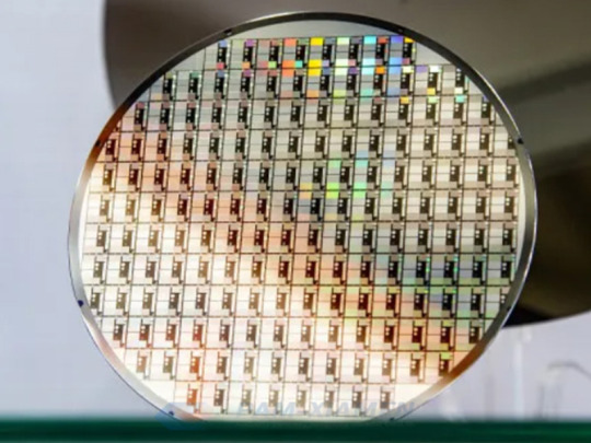
PAM XIAMEN offers GaN HEMT Epitaxial Wafers.

CZT wafer
Gallium Nitride (GaN) epitaxial wafers (epi-wafers). GaN high-electron-mobility transistors (HEMT) wafers on different substrates such as silicon essence, blue substrate, silicon carbide (SiC) substrate.
CZT wafer
We offer straight from the factory, along with therefore can offer the most effective prices on the industry for good quality GaN HEMT epi-wafers. Consumers from just about all over the world have got trustworthy PAM XIAMEN Products being a preferred supplier connected with GaN epi-wafers and GaN diffusion.
AlGaN/GaN HEMT upon only two in Conductive Semblable Wafer (GaN/SiC)
AlGaN/GaN HEMT in 2 in Blue Wafer
AlGaN/GaN HEMT about 3 inch Semi-Insulating Pareil Wafer (GaN/SiC)
AlGaN/GaN HEMT with 2 inch Mais Wafer (GaN/Si)
For a lot more information, please visit internet site: https://www.powerwaywafer.com,
send us e mail at sales@powerwaywafer. com in addition to powerwaymaterial@gmail. com
Found inside 1990, Xiamen Powerway Innovative Substance Co., Ltd (PAM-XIAMEN) is actually a leading manufacturer associated with semiconductor material in The far east. PAM-XIAMEN develops advanced ravenscroft progress and epitaxy technological innovation, making processes, engineered substrates as well as semiconductor devices. PAM-XIAMEN’s engineering enable higher efficiency and also lower cost developing of semiconductor wafer.
Top quality is the first top priority. PAM-XIAMEN have been ISO9001: '08, owns along with shares several modern facories which can easily provide quite a huge variety of qualified products to be able to meet diverse needs regarding our customers, each buy has to be managed by means of our rigorous top quality method. Test report will be presented to each shipment, in addition to each wafer are warrantee.
1 note
·
View note
Text
Gallium Arsenide (GaAs) Market Size Forecast to Reach $632.2 Billion by 2026
Gallium Arsenide (GaAs) Market Size is forecast to reach $632.2 billion by 2026, growing at a CAGR of 7.1% during 2021-2026. GaAs is increasingly used as a replacement for silicon because of its enhanced electronic properties and was selectively grown on GaAs substrates patterned with SiO2 by conventional molecular beam epitaxy. Moreover growing demand for GaAs across various end-user industries such as aerospace & defense, electronics, and communications is analyzed to drive the Gallium Arsenide Market share. In addition, owing to a wide direct band gap material that resists radiation damage, GaAs is an excellent option for outer space electronics and optical windows in high power applications. Further, other key factors driving the growth of the GaAs market include increase in adoption of 5G networks across the world and the advent of IoT has been one of the major reasons responsible for the growing trend of the Gallium Arsenide market size. The technology has given rise to a demand for high-frequency communication devices made with GaAs based ICs. Furthermore, this remarkable growth in the Gallium Arsenide market is providing a huge number of opportunities for wafer, EPI wafer & metal-organic chemical vapor deposition equipment suppliers, and manufacturers in the forecast period 2021-2026.
Request for Sample Report @ https://www.industryarc.com/pdfdownload.php?id=509501
Report Price: $ 5900 (Single User License)
Gallium Arsenide Market Segment Analysis - By Type
Vertical Gradient Freeze (VGF) Grown GaAs segment held significant market share of 40.5% in 2020. VGF Grown GaAs will remain the largest manufacturing technology, and it is expected to witness highest growth during the forecast period as it produces substrates with relatively low defect densities and higher mechanical strength. Vertical gradient freeze (VGF) technology is a proven technique for growing semiconductors composed of multiple elements that include gallium, arsenic, indium, and phosphorus. Such semiconductors offer capabilities that exceed those of wafers created on a single crystal silicon substrate. The main advantages of the VGF process include its scalability, low stress, high mechanical strength, and a defect rate that is orders of magnitude lower than conventional compound semiconductor crystal growth processes. Hence these benefits are analysed to drive the growth rate of the gallium arsenide market in the forecast period 2021-2026.
Gallium Arsenide Market Segment Analysis - By Application
Smart phones segment in Gallium Arsenide market is expected to witness a highest CAGR of 8.5% the forecast period. The demand for Gallium Arsenide is driven by smartphones and other applications across the consumer electronics industry, which require semiconductor ICs. In addition, increasing numbers of Internet of Things (IoT) devices is expected to force the semiconductor industry to invest in this equipment, in a bid to attain intelligent products. Moreover, the continuous advancements in consumer electronics and the use of sensors in various electronic products are proliferating the applications of plasma etching in smartphones and their demand across almost all the industry sectors. In 2018, the South Korean government announced to invest $1.34 billion for the next ten years to support the development of next-generation semiconductor technology, to support Samsung Electronics and SK Hynix. The investment will help Korean companies, such as Samsung and SK Hynix, to enhance their semiconductor manufacturing capabilities. Further with the powerful 5G cellular network being introduced to the world in 2019, mobile devices need a semiconductor that can handle the faster signal speed. As Gallium Arsenide will outperform silicon wafers due to its ultra-high frequency applications will enhance the demand for Gallium Arsenide industry in the forecast period 2021-2026.
Gallium Arsenide Market Segment Analysis - By Geography
Gallium Arsenide market in Asia-Pacific region held significant market share of 36.5% in 2020, owing to growing consumption of smartphones and other high-performance electronics devices in the region. Countries such as India, China, Taiwan, South Korea and so on are few of the prominent markets for Gallium Arsenide, and this is primarily attributed to the growing demand for advanced technologies across numerous end-user industries, high growth of the consumer electronics industry, rising support for the semiconductor industry in the region. In May 2019, Taiwan Semiconductor has opened new branch in Beijing to accommodate the rapid growth in China and engage local talent in its business development efforts. Moreover, the emergence of new technologies in Asia-Pacific has boosted the demand for innovative and user-friendly smart devices. There has been a rising demand from South Korea and Taiwan for semiconductor wafers, due to the large production of consumer electronic devices such as televisions, smartphones, PCs and so on. Further governments of several countries in this region are supporting the growth of semiconductor production by various initiatives, for instance, Made in Chine 2025, Make in India and others will promote the growth of semiconductor industries thereby increasing the growth of Gallium Arsenide market in the forecast period 2021-2026.
Inquiry Before Buying @ https://www.industryarc.com/reports/request-quote?id=509501
Gallium Arsenide Market Drivers
Growing Penetration of 5G
With the powerful 5G cellular network being introduced to the world in 2019, mobile devices need a semiconductor that can handle the faster signal speed. Gallium Arsenide due to its ultra-high frequency applications able to outperform silicon wafers in some of the most important ways. Moreover, with the emergence of 5G, silicon usage in semiconductors will be further reduced. Further for the implementation of 5G network, GaAs can be seen as the next generation of integrated circuits due to its high band gap, which drastically outperforms silicon. According to semiconductor Association, it is expected that the overall market for semiconductors could pass a whopping $20 trillion by 2025. This will create significant demand for GaAs in the forecast period. Furthermore governments of several countries have been investing heavily for the deployment of 5G. In 2019, China is expected to invest over $150 billion in its 5G networks through 2025. Similarly, Germany made a step towards accelerating the development of 5G services in the country, pouring additional investments into backing domestic endeavours. Hence growing penetration of 5g will drive the Gallium Arsenide Market growth in the forecast period 2021-2026.
Growth of Semiconductor industry creates significant demand for Gallium Arsenide Market
Growth of semiconductor manufacturing is analysed to create significant opportunities in the forecast period. In 2020, Indian Government is planning to offer around $1 billion in cash to every company that sets up a chip manufacturing unit in India. Similarly, China’s ‘Made in China 2025’ initiative will also create significant demand for semiconductor manufacturing in the forecast period. Moreover, U.S government is also committed to invest around $50 billion for the growth of semiconductor industry. Silicon is the most important material for semiconductor electronics. Silicon devices and integrated circuits are dominant in most applications from consumer electronics to automotive. However, in certain areas, silicon is being challenged by other semiconductor materials, such as gallium arsenide. Gallium arsenide excels in ultra-high frequency applications and has emerged as leading contenders for ultrahigh speed applications in the next generation of supercomputers and communication equipment. Hence Gallium arsenide has become relatively important and is expected to increase sharply in the forecast period 2021-2026.
Gallium Arsenide Market Challenges
High Production Cost
Although Gallium Arsenide market is growing at a significant phase it poses some difficulties, compared with that of silicon. For instance, unlike silicon, there is no natural oxide that acts as a mask to produce simple elements of the Complementary Metal Oxide Semiconductor (CMOS) logic style. High production cost of Gallium Arsenide act as major threat for the growth of the market. This is partly due to this technology not being able to achieve high volumes to bring the cost down and in a large part also because of not having a straightforward way to bring costs down generation after generation by exploiting device scaling like CMOS. Further GaAs technology does not easily lend itself to integrating millions or billions of transistors on one integrated circuit. Most GaAs ICs can manage to integrate only a handful of transistors unlike silicon. Hence these challenges hamper the market growth in the forecast period 2021-2026.
Gallium Arsenide Market Landscape
Product launches, acquisitions, Partnerships and R&D activities are key strategies adopted by players in the Gallium Arsenide market. Gallium Arsenide top 10 companies include Advanced Wireless Semiconductor Co., AXT Inc., Freiberger Compound Materials GmbH, GCS Holdings Inc., IntelliEPI Inc., IQE Plc, OMMIC SAS, Qorvo Inc., WIN Semiconductors Corp., and Xiamen Power way Advanced Material Co. Ltd. among others.
Acquisitions/Product Launches
In 2021 AXT, Inc., a leading manufacturer of compound semiconductor substrate wafers, has developed and shipped its first 8-inch diameter gallium arsenide (GaAs) substrates to a major customer. The 8-inch GaAs substrates, which are silicon doped, n-type substrates, demonstrate low etch pit densities (EPD) and low levels of slip lines.
In 2019, PAM-XIAMEN develops advanced crystal growth and epitaxy technologies, range from the first generation Germanium wafer, second-generation Gallium Arsenide with substrate growth and epitaxy on III-V silicon doped n-type semiconductor materials based on Ga, Al, In, As and P grown by MBE or MOCVD, to the third generation Silicon carbide and Gallium Nitride for LED and power device application.
Key Takeaways
Gallium Arsenide market in Asia-Pacific region held significant market share of 36.5% in 2020, owing to growing consumption of smartphones and other high-performance electronics devices in the region.
Vertical Gradient Freeze (VGF) Grown GaAs will remain the largest manufacturing technology, and it is expected to witness highest growth during the forecast period as it produces substrates with relatively low defect densities and higher mechanical strength
The demand for Gallium Arsenide is driven by smartphones and other applications across the consumer electronics industry, which require semiconductor ICs. In addition, the trend of increasing numbers of Internet of Things (IoT) devices is expected to force the semiconductor industry to invest in this equipment, in a bid to attain intelligent products.
Gallium Arsenide companies are strengthening their position through mergers & acquisitions and continuously investing in research and development (R&D) activities to come up with solutions to cater to the changing requirements of customers.
Related Reports
A.Semiconductor Market
https://www.industryarc.com/Report/18466/semiconductor-market-research-report-analysis.html
B.Compound Semiconductor Market
https://www.industryarc.com/Research/Compound-Semiconductor-Market-Research-507438
For more Electronics Market reports, please click here
About IndustryARC Market Research Reports
IndustryARC is a Research and Consulting Firm that publishes more than 500 reports annually, in various industries such as Agriculture, Automotive, Automation & Instrumentation, Chemicals and Materials, Energy and Power, Electronics, Food & Beverages, Information Technology, and Life sciences &Healthcare.
IndustryARC primarily focuses on cutting edge technologies and newer Applications in a Market. Our Custom Research Services are designed to provide insights on the constant flux in the global supply-demand gap of markets. Our strong team of analysts enables us to meet the client research needs at a rapid speed, with a variety of options for your business.
We look forward to support the client to be able to better address their customer needs, stay ahead in the market, become the top competitor and get real-time recommendations on business strategies and deals. Contact us to find out how we can help you today.
More about IndustryARC Market Research Reports
0 notes
Text
Gallium Arsenide (GaAs) Market Size Forecast to Reach $632.2 Billion by 2026
Gallium Arsenide (GaAs) Market Size is forecast to reach $632.2 billion by 2026, growing at a CAGR of 7.1% during 2021-2026. GaAs is increasingly used as a replacement for silicon because of its enhanced electronic properties and was selectively grown on GaAs substrates patterned with SiO2 by conventional molecular beam epitaxy. Moreover growing demand for GaAs across various end-user industries such as aerospace & defense, electronics, and communications is analyzed to drive the Gallium Arsenide Market share. In addition, owing to a wide direct band gap material that resists radiation damage, GaAs is an excellent option for outer space electronics and optical windows in high power applications. Further, other key factors driving the growth of the GaAs market include increase in adoption of 5G networks across the world and the advent of IoT has been one of the major reasons responsible for the growing trend of the Gallium Arsenide market size. The technology has given rise to a demand for high-frequency communication devices made with GaAs based ICs. Furthermore, this remarkable growth in the Gallium Arsenide market is providing a huge number of opportunities for wafer, EPI wafer & metal-organic chemical vapor deposition equipment suppliers, and manufacturers in the forecast period 2021-2026.
Request for Sample Report @ https://www.industryarc.com/pdfdownload.php?id=509501
Report Price: $ 5900 (Single User License)
Gallium Arsenide Market Segment Analysis - By Type
Vertical Gradient Freeze (VGF) Grown GaAs segment held significant market share of 40.5% in 2020. VGF Grown GaAs will remain the largest manufacturing technology, and it is expected to witness highest growth during the forecast period as it produces substrates with relatively low defect densities and higher mechanical strength. Vertical gradient freeze (VGF) technology is a proven technique for growing semiconductors composed of multiple elements that include gallium, arsenic, indium, and phosphorus. Such semiconductors offer capabilities that exceed those of wafers created on a single crystal silicon substrate. The main advantages of the VGF process include its scalability, low stress, high mechanical strength, and a defect rate that is orders of magnitude lower than conventional compound semiconductor crystal growth processes. Hence these benefits are analysed to drive the growth rate of the gallium arsenide market in the forecast period 2021-2026.
Gallium Arsenide Market Segment Analysis - By Application
Smart phones segment in Gallium Arsenide market is expected to witness a highest CAGR of 8.5% the forecast period. The demand for Gallium Arsenide is driven by smartphones and other applications across the consumer electronics industry, which require semiconductor ICs. In addition, increasing numbers of Internet of Things (IoT) devices is expected to force the semiconductor industry to invest in this equipment, in a bid to attain intelligent products. Moreover, the continuous advancements in consumer electronics and the use of sensors in various electronic products are proliferating the applications of plasma etching in smartphones and their demand across almost all the industry sectors. In 2018, the South Korean government announced to invest $1.34 billion for the next ten years to support the development of next-generation semiconductor technology, to support Samsung Electronics and SK Hynix. The investment will help Korean companies, such as Samsung and SK Hynix, to enhance their semiconductor manufacturing capabilities. Further with the powerful 5G cellular network being introduced to the world in 2019, mobile devices need a semiconductor that can handle the faster signal speed. As Gallium Arsenide will outperform silicon wafers due to its ultra-high frequency applications will enhance the demand for Gallium Arsenide industry in the forecast period 2021-2026.
Gallium Arsenide Market Segment Analysis - By Geography
Gallium Arsenide market in Asia-Pacific region held significant market share of 36.5% in 2020, owing to growing consumption of smartphones and other high-performance electronics devices in the region. Countries such as India, China, Taiwan, South Korea and so on are few of the prominent markets for Gallium Arsenide, and this is primarily attributed to the growing demand for advanced technologies across numerous end-user industries, high growth of the consumer electronics industry, rising support for the semiconductor industry in the region. In May 2019, Taiwan Semiconductor has opened new branch in Beijing to accommodate the rapid growth in China and engage local talent in its business development efforts. Moreover, the emergence of new technologies in Asia-Pacific has boosted the demand for innovative and user-friendly smart devices. There has been a rising demand from South Korea and Taiwan for semiconductor wafers, due to the large production of consumer electronic devices such as televisions, smartphones, PCs and so on. Further governments of several countries in this region are supporting the growth of semiconductor production by various initiatives, for instance, Made in Chine 2025, Make in India and others will promote the growth of semiconductor industries thereby increasing the growth of Gallium Arsenide market in the forecast period 2021-2026.
Inquiry Before Buying @ https://www.industryarc.com/reports/request-quote?id=509501
Gallium Arsenide Market Drivers
Growing Penetration of 5G
With the powerful 5G cellular network being introduced to the world in 2019, mobile devices need a semiconductor that can handle the faster signal speed. Gallium Arsenide due to its ultra-high frequency applications able to outperform silicon wafers in some of the most important ways. Moreover, with the emergence of 5G, silicon usage in semiconductors will be further reduced. Further for the implementation of 5G network, GaAs can be seen as the next generation of integrated circuits due to its high band gap, which drastically outperforms silicon. According to semiconductor Association, it is expected that the overall market for semiconductors could pass a whopping $20 trillion by 2025. This will create significant demand for GaAs in the forecast period. Furthermore governments of several countries have been investing heavily for the deployment of 5G. In 2019, China is expected to invest over $150 billion in its 5G networks through 2025. Similarly, Germany made a step towards accelerating the development of 5G services in the country, pouring additional investments into backing domestic endeavours. Hence growing penetration of 5g will drive the Gallium Arsenide Market growth in the forecast period 2021-2026.
Growth of Semiconductor industry creates significant demand for Gallium Arsenide Market
Growth of semiconductor manufacturing is analysed to create significant opportunities in the forecast period. In 2020, Indian Government is planning to offer around $1 billion in cash to every company that sets up a chip manufacturing unit in India. Similarly, China’s ‘Made in China 2025’ initiative will also create significant demand for semiconductor manufacturing in the forecast period. Moreover, U.S government is also committed to invest around $50 billion for the growth of semiconductor industry. Silicon is the most important material for semiconductor electronics. Silicon devices and integrated circuits are dominant in most applications from consumer electronics to automotive. However, in certain areas, silicon is being challenged by other semiconductor materials, such as gallium arsenide. Gallium arsenide excels in ultra-high frequency applications and has emerged as leading contenders for ultrahigh speed applications in the next generation of supercomputers and communication equipment. Hence Gallium arsenide has become relatively important and is expected to increase sharply in the forecast period 2021-2026.
Gallium Arsenide Market Challenges
High Production Cost
Although Gallium Arsenide market is growing at a significant phase it poses some difficulties, compared with that of silicon. For instance, unlike silicon, there is no natural oxide that acts as a mask to produce simple elements of the Complementary Metal Oxide Semiconductor (CMOS) logic style. High production cost of Gallium Arsenide act as major threat for the growth of the market. This is partly due to this technology not being able to achieve high volumes to bring the cost down and in a large part also because of not having a straightforward way to bring costs down generation after generation by exploiting device scaling like CMOS. Further GaAs technology does not easily lend itself to integrating millions or billions of transistors on one integrated circuit. Most GaAs ICs can manage to integrate only a handful of transistors unlike silicon. Hence these challenges hamper the market growth in the forecast period 2021-2026.
Gallium Arsenide Market Landscape
Product launches, acquisitions, Partnerships and R&D activities are key strategies adopted by players in the Gallium Arsenide market. Gallium Arsenide top 10 companies include Advanced Wireless Semiconductor Co., AXT Inc., Freiberger Compound Materials GmbH, GCS Holdings Inc., IntelliEPI Inc., IQE Plc, OMMIC SAS, Qorvo Inc., WIN Semiconductors Corp., and Xiamen Power way Advanced Material Co. Ltd. among others.
Acquisitions/Product Launches
In 2021 AXT, Inc., a leading manufacturer of compound semiconductor substrate wafers, has developed and shipped its first 8-inch diameter gallium arsenide (GaAs) substrates to a major customer. The 8-inch GaAs substrates, which are silicon doped, n-type substrates, demonstrate low etch pit densities (EPD) and low levels of slip lines.
In 2019, PAM-XIAMEN develops advanced crystal growth and epitaxy technologies, range from the first generation Germanium wafer, second-generation Gallium Arsenide with substrate growth and epitaxy on III-V silicon doped n-type semiconductor materials based on Ga, Al, In, As and P grown by MBE or MOCVD, to the third generation Silicon carbide and Gallium Nitride for LED and power device application.
Key Takeaways
Gallium Arsenide market in Asia-Pacific region held significant market share of 36.5% in 2020, owing to growing consumption of smartphones and other high-performance electronics devices in the region.
Vertical Gradient Freeze (VGF) Grown GaAs will remain the largest manufacturing technology, and it is expected to witness highest growth during the forecast period as it produces substrates with relatively low defect densities and higher mechanical strength
The demand for Gallium Arsenide is driven by smartphones and other applications across the consumer electronics industry, which require semiconductor ICs. In addition, the trend of increasing numbers of Internet of Things (IoT) devices is expected to force the semiconductor industry to invest in this equipment, in a bid to attain intelligent products.
Gallium Arsenide companies are strengthening their position through mergers & acquisitions and continuously investing in research and development (R&D) activities to come up with solutions to cater to the changing requirements of customers.
0 notes
Text
Gallium Arsenide Market - Industry Analysis, Market Size, Share, Trends, Application Analysis, Growth And Forecast 2021 - 2026
Gallium Arsenide (GaAs) Market Size is forecast to reach $632.2 billion by 2026, growing at a CAGR of 7.1% during 2021-2026. GaAs is increasingly used as a replacement for silicon because of its enhanced electronic properties and was selectively grown on GaAs substrates patterned with SiO2 by conventional molecular beam epitaxy. Moreover growing demand for GaAs across various end-user industries such as aerospace & defense, electronics, and communications is analyzed to drive the Gallium Arsenide Market share. In addition, owing to a wide direct band gap material that resists radiation damage, GaAs is an excellent option for outer space electronics and optical windows in high power applications. Further, other key factors driving the growth of the GaAs market include increase in adoption of 5G networks across the world and the advent of IoT has been one of the major reasons responsible for the growing trend of the Gallium Arsenide market size. The technology has given rise to a demand for high-frequency communication devices made with GaAs based ICs. Furthermore, this remarkable growth in the Gallium Arsenide market is providing a huge number of opportunities for wafer, EPI wafer & metal-organic chemical vapor deposition equipment suppliers, and manufacturers in the forecast period 2021-2026.
Gallium Arsenide Market Report Coverage
The report: “Gallium Arsenide Market Report– Forecast (2021-2026)”, by IndustryARC covers an in-depth analysis of the following segments of the Gallium Arsenide market
By Type: Liquid Encapsulated Czochralski Grown GaAs, Vertical Gradient Freeze (VGF) Grown GaAs, Others
By Application: Smartphones, Computer, Photovoltaic Cells, Laser Diodes, Infrared Emission, Automotive Electronics, Military Area, Wireless Communication, Optoelectronic Devices, Other.
By Geography: North America (U.S, Canada, Mexico), South America(Brazil, Argentina and others), Europe(Germany, UK, France, Italy, Spain, Russia and Others), APAC(China, Japan India, SK, Aus and Others), and RoW (Middle East and Africa)
Key Takeaways
Gallium Arsenide market in Asia-Pacific region held significant market share of 36.5% in 2020, owing to growing consumption of smartphones and other high-performance electronics devices in the region.
Vertical Gradient Freeze (VGF) Grown GaAs will remain the largest manufacturing technology, and it is expected to witness highest growth during the forecast period as it produces substrates with relatively low defect densities and higher mechanical strength
The demand for Gallium Arsenide is driven by smartphones and other applications across the consumer electronics industry, which require semiconductor ICs. In addition, the trend of increasing numbers of Internet of Things (IoT) devices is expected to force the semiconductor industry to invest in this equipment, in a bid to attain intelligent products.
Gallium Arsenide companies are strengthening their position through mergers & acquisitions and continuously investing in research and development (R&D) activities to come up with solutions to cater to the changing requirements of customers.
Global Gallium Arsenide Market, By Region, 2020
For More Details on This Report - Request for Sample
Gallium Arsenide Market Segment Analysis - By Type
Vertical Gradient Freeze (VGF) Grown GaAs segment held significant market share of 40.5% in 2020. VGF Grown GaAs will remain the largest manufacturing technology, and it is expected to witness highest growth during the forecast period as it produces substrates with relatively low defect densities and higher mechanical strength. Vertical gradient freeze (VGF) technology is a proven technique for growing semiconductors composed of multiple elements that include gallium, arsenic, indium, and phosphorus. Such semiconductors offer capabilities that exceed those of wafers created on a single crystal silicon substrate. The main advantages of the VGF process include its scalability, low stress, high mechanical strength, and a defect rate that is orders of magnitude lower than conventional compound semiconductor crystal growth processes. Hence these benefits are analysed to drive the growth rate of the gallium arsenide market in the forecast period 2021-2026.
Gallium Arsenide Market Segment Analysis - By Application
Smart phones segment in Gallium Arsenide market is expected to witness a highest CAGR of 8.5% the forecast period. The demand for Gallium Arsenide is driven by smartphones and other applications across the consumer electronics industry, which require semiconductor ICs. In addition, increasing numbers of Internet of Things (IoT) devices is expected to force the semiconductor industry to invest in this equipment, in a bid to attain intelligent products. Moreover, the continuous advancements in consumer electronics and the use of sensors in various electronic products are proliferating the applications of plasma etching in smartphones and their demand across almost all the industry sectors. In 2018, the South Korean government announced to invest $1.34 billion for the next ten years to support the development of next-generation semiconductor technology, to support Samsung Electronics and SK Hynix. The investment will help Korean companies, such as Samsung and SK Hynix, to enhance their semiconductor manufacturing capabilities. Further with the powerful 5G cellular network being introduced to the world in 2019, mobile devices need a semiconductor that can handle the faster signal speed. As Gallium Arsenide will outperform silicon wafers due to its ultra-high frequency applications will enhance the demand for Gallium Arsenide industry in the forecast period 2021-2026.
Gallium Arsenide Market Segment Analysis - By Geography
Gallium Arsenide market in Asia-Pacific region held significant market share of 36.5% in 2020, owing to growing consumption of smartphones and other high-performance electronics devices in the region. Countries such as India, China, Taiwan, South Korea and so on are few of the prominent markets for Gallium Arsenide, and this is primarily attributed to the growing demand for advanced technologies across numerous end-user industries, high growth of the consumer electronics industry, rising support for the semiconductor industry in the region. In May 2019, Taiwan Semiconductor has opened new branch in Beijing to accommodate the rapid growth in China and engage local talent in its business development efforts. Moreover, the emergence of new technologies in Asia-Pacific has boosted the demand for innovative and user-friendly smart devices. There has been a rising demand from South Korea and Taiwan for semiconductor wafers, due to the large production of consumer electronic devices such as televisions, smartphones, PCs and so on. Further governments of several countries in this region are supporting the growth of semiconductor production by various initiatives, for instance, Made in Chine 2025, Make in India and others will promote the growth of semiconductor industries thereby increasing the growth of Gallium Arsenide market in the forecast period 2021-2026.
Gallium Arsenide Market Drivers
Growing Penetration of 5G
With the powerful 5G cellular network being introduced to the world in 2019, mobile devices need a semiconductor that can handle the faster signal speed. Gallium Arsenide due to its ultra-high frequency applications able to outperform silicon wafers in some of the most important ways. Moreover, with the emergence of 5G, silicon usage in semiconductors will be further reduced. Further for the implementation of 5G network, GaAs can be seen as the next generation of integrated circuits due to its high band gap, which drastically outperforms silicon. According to semiconductor Association, it is expected that the overall market for semiconductors could pass a whopping $20 trillion by 2025. This will create significant demand for GaAs in the forecast period. Furthermore governments of several countries have been investing heavily for the deployment of 5G. In 2019, China is expected to invest over $150 billion in its 5G networks through 2025. Similarly, Germany made a step towards accelerating the development of 5G services in the country, pouring additional investments into backing domestic endeavours. Hence growing penetration of 5g will drive the Gallium Arsenide Market growth in the forecast period 2021-2026.
Growth of Semiconductor industry creates significant demand for Gallium Arsenide Market
Growth of semiconductor manufacturing is analysed to create significant opportunities in the forecast period. In 2020, Indian Government is planning to offer around $1 billion in cash to every company that sets up a chip manufacturing unit in India. Similarly, China’s ‘Made in China 2025’ initiative will also create significant demand for semiconductor manufacturing in the forecast period. Moreover, U.S government is also committed to invest around $50 billion for the growth of semiconductor industry. Silicon is the most important material for semiconductor electronics. Silicon devices and integrated circuits are dominant in most applications from consumer electronics to automotive. However, in certain areas, silicon is being challenged by other semiconductor materials, such as gallium arsenide. Gallium arsenide excels in ultra-high frequency applications and has emerged as leading contenders for ultrahigh speed applications in the next generation of supercomputers and communication equipment. Hence Gallium arsenide has become relatively important and is expected to increase sharply in the forecast period 2021-2026.
Gallium Arsenide Market Challenges
High Production Cost
Although Gallium Arsenide market is growing at a significant phase it poses some difficulties, compared with that of silicon. For instance, unlike silicon, there is no natural oxide that acts as a mask to produce simple elements of the Complementary Metal Oxide Semiconductor (CMOS) logic style. High production cost of Gallium Arsenide act as major threat for the growth of the market. This is partly due to this technology not being able to achieve high volumes to bring the cost down and in a large part also because of not having a straightforward way to bring costs down generation after generation by exploiting device scaling like CMOS. Further GaAs technology does not easily lend itself to integrating millions or billions of transistors on one integrated circuit. Most GaAs ICs can manage to integrate only a handful of transistors unlike silicon. Hence these challenges hamper the market growth in the forecast period 2021-2026.
Gallium Arsenide Market Landscape
Product launches, acquisitions, Partnerships and R&D activities are key strategies adopted by players in the Gallium Arsenide market. Gallium Arsenide top 10 companies include Advanced Wireless Semiconductor Co., AXT Inc., Freiberger Compound Materials GmbH, GCS Holdings Inc., IntelliEPI Inc., IQE Plc, OMMIC SAS, Qorvo Inc., WIN Semiconductors Corp., and Xiamen Power way Advanced Material Co. Ltd. among others.
Acquisitions/Product Launches
In 2021 AXT, Inc., a leading manufacturer of compound semiconductor substrate wafers, has developed and shipped its first 8-inch diameter gallium arsenide (GaAs) substrates to a major customer. The 8-inch GaAs substrates, which are silicon doped, n-type substrates, demonstrate low etch pit densities (EPD) and low levels of slip lines.
In 2019, PAM-XIAMEN develops advanced crystal growth and epitaxy technologies, range from the first generation Germanium wafer, second-generation Gallium Arsenide with substrate growth and epitaxy on III-V silicon doped n-type semiconductor materials based on Ga, Al, In, As and P grown by MBE or MOCVD, to the third generation Silicon carbide and Gallium Nitride for LED and power device application.
Relevant Report Titles:
Semiconductor Market:
Report Code: ESR 0563
Compound Semiconductor Market:
Report Code: ESR 87979
For more Electronics Market reports, please click here
0 notes
Text
Gallium Arsenide Market Size is forecast to reach $632.2 billion by 2026, growing at a CAGR of 7.1% during 2021-2026.
Gallium Arsenide (GaAs) Market Size is forecast to reach $632.2 billion by 2026, growing at a CAGR of 7.1% during 2021-2026. GaAs is increasingly used as a replacement for silicon because of its enhanced electronic properties and was selectively grown on GaAs substrates patterned with SiO2 by conventional molecular beam epitaxy. Moreover growing demand for GaAs across various end-user industries such as aerospace & defense, electronics, and communications is analyzed to drive the Gallium Arsenide Market share. In addition, owing to a wide direct band gap material that resists radiation damage, GaAs is an excellent option for outer space electronics and optical windows in high power applications. Further, other key factors driving the growth of the GaAs market include increase in adoption of 5G networks across the world and the advent of IoT has been one of the major reasons responsible for the growing trend of the Gallium Arsenide market size. The technology has given rise to a demand for high-frequency communication devices made with GaAs based ICs. Furthermore, this remarkable growth in the Gallium Arsenide market is providing a huge number of opportunities for wafer, EPI wafer & metal-organic chemical vapor deposition equipment suppliers, and manufacturers in the forecast period 2021-2026.
Request for Sample Report @ https://www.industryarc.com/pdfdownload.php?id=509501
Report Price: $ 5900 (Single User License)
Gallium Arsenide Market Segment Analysis - By Type
Vertical Gradient Freeze (VGF) Grown GaAs segment held significant market share of 40.5% in 2020. VGF Grown GaAs will remain the largest manufacturing technology, and it is expected to witness highest growth during the forecast period as it produces substrates with relatively low defect densities and higher mechanical strength. Vertical gradient freeze (VGF) technology is a proven technique for growing semiconductors composed of multiple elements that include gallium, arsenic, indium, and phosphorus. Such semiconductors offer capabilities that exceed those of wafers created on a single crystal silicon substrate. The main advantages of the VGF process include its scalability, low stress, high mechanical strength, and a defect rate that is orders of magnitude lower than conventional compound semiconductor crystal growth processes. Hence these benefits are analysed to drive the growth rate of the gallium arsenide market in the forecast period 2021-2026.
Gallium Arsenide Market Segment Analysis - By Application
Smart phones segment in Gallium Arsenide market is expected to witness a highest CAGR of 8.5% the forecast period. The demand for Gallium Arsenide is driven by smartphones and other applications across the consumer electronics industry, which require semiconductor ICs. In addition, increasing numbers of Internet of Things (IoT) devices is expected to force the semiconductor industry to invest in this equipment, in a bid to attain intelligent products. Moreover, the continuous advancements in consumer electronics and the use of sensors in various electronic products are proliferating the applications of plasma etching in smartphones and their demand across almost all the industry sectors. In 2018, the South Korean government announced to invest $1.34 billion for the next ten years to support the development of next-generation semiconductor technology, to support Samsung Electronics and SK Hynix. The investment will help Korean companies, such as Samsung and SK Hynix, to enhance their semiconductor manufacturing capabilities. Further with the powerful 5G cellular network being introduced to the world in 2019, mobile devices need a semiconductor that can handle the faster signal speed. As Gallium Arsenide will outperform silicon wafers due to its ultra-high frequency applications will enhance the demand for Gallium Arsenide industry in the forecast period 2021-2026.
Gallium Arsenide Market Segment Analysis - By Geography
Gallium Arsenide market in Asia-Pacific region held significant market share of 36.5% in 2020, owing to growing consumption of smartphones and other high-performance electronics devices in the region. Countries such as India, China, Taiwan, South Korea and so on are few of the prominent markets for Gallium Arsenide, and this is primarily attributed to the growing demand for advanced technologies across numerous end-user industries, high growth of the consumer electronics industry, rising support for the semiconductor industry in the region. In May 2019, Taiwan Semiconductor has opened new branch in Beijing to accommodate the rapid growth in China and engage local talent in its business development efforts. Moreover, the emergence of new technologies in Asia-Pacific has boosted the demand for innovative and user-friendly smart devices. There has been a rising demand from South Korea and Taiwan for semiconductor wafers, due to the large production of consumer electronic devices such as televisions, smartphones, PCs and so on. Further governments of several countries in this region are supporting the growth of semiconductor production by various initiatives, for instance, Made in Chine 2025, Make in India and others will promote the growth of semiconductor industries thereby increasing the growth of Gallium Arsenide market in the forecast period 2021-2026.
Inquiry Before Buying @ https://www.industryarc.com/reports/request-quote?id=509501
Gallium Arsenide Market Drivers
Growing Penetration of 5G
With the powerful 5G cellular network being introduced to the world in 2019, mobile devices need a semiconductor that can handle the faster signal speed. Gallium Arsenide due to its ultra-high frequency applications able to outperform silicon wafers in some of the most important ways. Moreover, with the emergence of 5G, silicon usage in semiconductors will be further reduced. Further for the implementation of 5G network, GaAs can be seen as the next generation of integrated circuits due to its high band gap, which drastically outperforms silicon. According to semiconductor Association, it is expected that the overall market for semiconductors could pass a whopping $20 trillion by 2025. This will create significant demand for GaAs in the forecast period. Furthermore governments of several countries have been investing heavily for the deployment of 5G. In 2019, China is expected to invest over $150 billion in its 5G networks through 2025. Similarly, Germany made a step towards accelerating the development of 5G services in the country, pouring additional investments into backing domestic endeavours. Hence growing penetration of 5g will drive the Gallium Arsenide Market growth in the forecast period 2021-2026.
Growth of Semiconductor industry creates significant demand for Gallium Arsenide Market
Growth of semiconductor manufacturing is analysed to create significant opportunities in the forecast period. In 2020, Indian Government is planning to offer around $1 billion in cash to every company that sets up a chip manufacturing unit in India. Similarly, China’s ‘Made in China 2025’ initiative will also create significant demand for semiconductor manufacturing in the forecast period. Moreover, U.S government is also committed to invest around $50 billion for the growth of semiconductor industry. Silicon is the most important material for semiconductor electronics. Silicon devices and integrated circuits are dominant in most applications from consumer electronics to automotive. However, in certain areas, silicon is being challenged by other semiconductor materials, such as gallium arsenide. Gallium arsenide excels in ultra-high frequency applications and has emerged as leading contenders for ultrahigh speed applications in the next generation of supercomputers and communication equipment. Hence Gallium arsenide has become relatively important and is expected to increase sharply in the forecast period 2021-2026.
Gallium Arsenide Market Challenges
High Production Cost
Although Gallium Arsenide market is growing at a significant phase it poses some difficulties, compared with that of silicon. For instance, unlike silicon, there is no natural oxide that acts as a mask to produce simple elements of the Complementary Metal Oxide Semiconductor (CMOS) logic style. High production cost of Gallium Arsenide act as major threat for the growth of the market. This is partly due to this technology not being able to achieve high volumes to bring the cost down and in a large part also because of not having a straightforward way to bring costs down generation after generation by exploiting device scaling like CMOS. Further GaAs technology does not easily lend itself to integrating millions or billions of transistors on one integrated circuit. Most GaAs ICs can manage to integrate only a handful of transistors unlike silicon. Hence these challenges hamper the market growth in the forecast period 2021-2026.
Gallium Arsenide Market Landscape
Product launches, acquisitions, Partnerships and R&D activities are key strategies adopted by players in the Gallium Arsenide market. Gallium Arsenide top 10 companies include Advanced Wireless Semiconductor Co., AXT Inc., Freiberger Compound Materials GmbH, GCS Holdings Inc., IntelliEPI Inc., IQE Plc, OMMIC SAS, Qorvo Inc., WIN Semiconductors Corp., and Xiamen Power way Advanced Material Co. Ltd. among others.
Acquisitions/Product Launches
In 2021 AXT, Inc., a leading manufacturer of compound semiconductor substrate wafers, has developed and shipped its first 8-inch diameter gallium arsenide (GaAs) substrates to a major customer. The 8-inch GaAs substrates, which are silicon doped, n-type substrates, demonstrate low etch pit densities (EPD) and low levels of slip lines.
In 2019, PAM-XIAMEN develops advanced crystal growth and epitaxy technologies, range from the first generation Germanium wafer, second-generation Gallium Arsenide with substrate growth and epitaxy on III-V silicon doped n-type semiconductor materials based on Ga, Al, In, As and P grown by MBE or MOCVD, to the third generation Silicon carbide and Gallium Nitride for LED and power device application.
Key Takeaways
Gallium Arsenide market in Asia-Pacific region held significant market share of 36.5% in 2020, owing to growing consumption of smartphones and other high-performance electronics devices in the region.
Vertical Gradient Freeze (VGF) Grown GaAs will remain the largest manufacturing technology, and it is expected to witness highest growth during the forecast period as it produces substrates with relatively low defect densities and higher mechanical strength
The demand for Gallium Arsenide is driven by smartphones and other applications across the consumer electronics industry, which require semiconductor ICs. In addition, the trend of increasing numbers of Internet of Things (IoT) devices is expected to force the semiconductor industry to invest in this equipment, in a bid to attain intelligent products.
Gallium Arsenide companies are strengthening their position through mergers & acquisitions and continuously investing in research and development (R&D) activities to come up with solutions to cater to the changing requirements of customers.
Related Reports
A.Semiconductor Market
https://www.industryarc.com/Report/18466/semiconductor-market-research-report-analysis.html
B.Compound Semiconductor Market
https://www.industryarc.com/Research/Compound-Semiconductor-Market-Research-507438
For more Electronics Market reports, please click here
0 notes
Text
Gallium Arsenide (GaAs) Market Size Forecast to Reach $632.2 Billion by 2026
Gallium Arsenide (GaAs) Market Size is forecast to reach $632.2 billion by 2026, growing at a CAGR of 7.1% during 2021-2026. GaAs is increasingly used as a replacement for silicon because of its enhanced electronic properties and was selectively grown on GaAs substrates patterned with SiO2 by conventional molecular beam epitaxy. Moreover growing demand for GaAs across various end-user industries such as aerospace & defense, electronics, and communications is analyzed to drive the Gallium Arsenide Market share. In addition, owing to a wide direct band gap material that resists radiation damage, GaAs is an excellent option for outer space electronics and optical windows in high power applications. Further, other key factors driving the growth of the GaAs market include increase in adoption of 5G networks across the world and the advent of IoT has been one of the major reasons responsible for the growing trend of the Gallium Arsenide market size. The technology has given rise to a demand for high-frequency communication devices made with GaAs based ICs. Furthermore, this remarkable growth in the Gallium Arsenide market is providing a huge number of opportunities for wafer, EPI wafer & metal-organic chemical vapor deposition equipment suppliers, and manufacturers in the forecast period 2021-2026.
Request for Sample Report @ https://www.industryarc.com/pdfdownload.php?id=509501
Report Price: $ 5900 (Single User License)
Gallium Arsenide Market Segment Analysis - By Type
Vertical Gradient Freeze (VGF) Grown GaAs segment held significant market share of 40.5% in 2020. VGF Grown GaAs will remain the largest manufacturing technology, and it is expected to witness highest growth during the forecast period as it produces substrates with relatively low defect densities and higher mechanical strength. Vertical gradient freeze (VGF) technology is a proven technique for growing semiconductors composed of multiple elements that include gallium, arsenic, indium, and phosphorus. Such semiconductors offer capabilities that exceed those of wafers created on a single crystal silicon substrate. The main advantages of the VGF process include its scalability, low stress, high mechanical strength, and a defect rate that is orders of magnitude lower than conventional compound semiconductor crystal growth processes. Hence these benefits are analysed to drive the growth rate of the gallium arsenide market in the forecast period 2021-2026.
Gallium Arsenide Market Segment Analysis - By Application
Smart phones segment in Gallium Arsenide market is expected to witness a highest CAGR of 8.5% the forecast period. The demand for Gallium Arsenide is driven by smartphones and other applications across the consumer electronics industry, which require semiconductor ICs. In addition, increasing numbers of Internet of Things (IoT) devices is expected to force the semiconductor industry to invest in this equipment, in a bid to attain intelligent products. Moreover, the continuous advancements in consumer electronics and the use of sensors in various electronic products are proliferating the applications of plasma etching in smartphones and their demand across almost all the industry sectors. In 2018, the South Korean government announced to invest $1.34 billion for the next ten years to support the development of next-generation semiconductor technology, to support Samsung Electronics and SK Hynix. The investment will help Korean companies, such as Samsung and SK Hynix, to enhance their semiconductor manufacturing capabilities. Further with the powerful 5G cellular network being introduced to the world in 2019, mobile devices need a semiconductor that can handle the faster signal speed. As Gallium Arsenide will outperform silicon wafers due to its ultra-high frequency applications will enhance the demand for Gallium Arsenide industry in the forecast period 2021-2026.
Gallium Arsenide Market Segment Analysis - By Geography
Gallium Arsenide market in Asia-Pacific region held significant market share of 36.5% in 2020, owing to growing consumption of smartphones and other high-performance electronics devices in the region. Countries such as India, China, Taiwan, South Korea and so on are few of the prominent markets for Gallium Arsenide, and this is primarily attributed to the growing demand for advanced technologies across numerous end-user industries, high growth of the consumer electronics industry, rising support for the semiconductor industry in the region. In May 2019, Taiwan Semiconductor has opened new branch in Beijing to accommodate the rapid growth in China and engage local talent in its business development efforts. Moreover, the emergence of new technologies in Asia-Pacific has boosted the demand for innovative and user-friendly smart devices. There has been a rising demand from South Korea and Taiwan for semiconductor wafers, due to the large production of consumer electronic devices such as televisions, smartphones, PCs and so on. Further governments of several countries in this region are supporting the growth of semiconductor production by various initiatives, for instance, Made in Chine 2025, Make in India and others will promote the growth of semiconductor industries thereby increasing the growth of Gallium Arsenide market in the forecast period 2021-2026.
Inquiry Before Buying @ https://www.industryarc.com/reports/request-quote?id=509501
Gallium Arsenide Market Drivers
Growing Penetration of 5G
With the powerful 5G cellular network being introduced to the world in 2019, mobile devices need a semiconductor that can handle the faster signal speed. Gallium Arsenide due to its ultra-high frequency applications able to outperform silicon wafers in some of the most important ways. Moreover, with the emergence of 5G, silicon usage in semiconductors will be further reduced. Further for the implementation of 5G network, GaAs can be seen as the next generation of integrated circuits due to its high band gap, which drastically outperforms silicon. According to semiconductor Association, it is expected that the overall market for semiconductors could pass a whopping $20 trillion by 2025. This will create significant demand for GaAs in the forecast period. Furthermore governments of several countries have been investing heavily for the deployment of 5G. In 2019, China is expected to invest over $150 billion in its 5G networks through 2025. Similarly, Germany made a step towards accelerating the development of 5G services in the country, pouring additional investments into backing domestic endeavours. Hence growing penetration of 5g will drive the Gallium Arsenide Market growth in the forecast period 2021-2026.
Growth of Semiconductor industry creates significant demand for Gallium Arsenide Market
Growth of semiconductor manufacturing is analysed to create significant opportunities in the forecast period. In 2020, Indian Government is planning to offer around $1 billion in cash to every company that sets up a chip manufacturing unit in India. Similarly, China’s ‘Made in China 2025’ initiative will also create significant demand for semiconductor manufacturing in the forecast period. Moreover, U.S government is also committed to invest around $50 billion for the growth of semiconductor industry. Silicon is the most important material for semiconductor electronics. Silicon devices and integrated circuits are dominant in most applications from consumer electronics to automotive. However, in certain areas, silicon is being challenged by other semiconductor materials, such as gallium arsenide. Gallium arsenide excels in ultra-high frequency applications and has emerged as leading contenders for ultrahigh speed applications in the next generation of supercomputers and communication equipment. Hence Gallium arsenide has become relatively important and is expected to increase sharply in the forecast period 2021-2026.
Gallium Arsenide Market Challenges
High Production Cost
Although Gallium Arsenide market is growing at a significant phase it poses some difficulties, compared with that of silicon. For instance, unlike silicon, there is no natural oxide that acts as a mask to produce simple elements of the Complementary Metal Oxide Semiconductor (CMOS) logic style. High production cost of Gallium Arsenide act as major threat for the growth of the market. This is partly due to this technology not being able to achieve high volumes to bring the cost down and in a large part also because of not having a straightforward way to bring costs down generation after generation by exploiting device scaling like CMOS. Further GaAs technology does not easily lend itself to integrating millions or billions of transistors on one integrated circuit. Most GaAs ICs can manage to integrate only a handful of transistors unlike silicon. Hence these challenges hamper the market growth in the forecast period 2021-2026.
Gallium Arsenide Market Landscape
Product launches, acquisitions, Partnerships and R&D activities are key strategies adopted by players in the Gallium Arsenide market. Gallium Arsenide top 10 companies include Advanced Wireless Semiconductor Co., AXT Inc., Freiberger Compound Materials GmbH, GCS Holdings Inc., IntelliEPI Inc., IQE Plc, OMMIC SAS, Qorvo Inc., WIN Semiconductors Corp., and Xiamen Power way Advanced Material Co. Ltd. among others.
Acquisitions/Product Launches
In 2021 AXT, Inc., a leading manufacturer of compound semiconductor substrate wafers, has developed and shipped its first 8-inch diameter gallium arsenide (GaAs) substrates to a major customer. The 8-inch GaAs substrates, which are silicon doped, n-type substrates, demonstrate low etch pit densities (EPD) and low levels of slip lines.
In 2019, PAM-XIAMEN develops advanced crystal growth and epitaxy technologies, range from the first generation Germanium wafer, second-generation Gallium Arsenide with substrate growth and epitaxy on III-V silicon doped n-type semiconductor materials based on Ga, Al, In, As and P grown by MBE or MOCVD, to the third generation Silicon carbide and Gallium Nitride for LED and power device application.
Key Takeaways
Gallium Arsenide market in Asia-Pacific region held significant market share of 36.5% in 2020, owing to growing consumption of smartphones and other high-performance electronics devices in the region.
Vertical Gradient Freeze (VGF) Grown GaAs will remain the largest manufacturing technology, and it is expected to witness highest growth during the forecast period as it produces substrates with relatively low defect densities and higher mechanical strength
The demand for Gallium Arsenide is driven by smartphones and other applications across the consumer electronics industry, which require semiconductor ICs. In addition, the trend of increasing numbers of Internet of Things (IoT) devices is expected to force the semiconductor industry to invest in this equipment, in a bid to attain intelligent products.
Gallium Arsenide companies are strengthening their position through mergers & acquisitions and continuously investing in research and development (R&D) activities to come up with solutions to cater to the changing requirements of customers.
Related Reports
A.Semiconductor Market
https://www.industryarc.com/Report/18466/semiconductor-market-research-report-analysis.html
B.Compound Semiconductor Market
https://www.industryarc.com/Research/Compound-Semiconductor-Market-Research-507438
For more Electronics Market reports, please click here
About IndustryARC Market Research Reports
IndustryARC is a Research and Consulting Firm that publishes more than 500 reports annually, in various industries such as Agriculture, Automotive, Automation & Instrumentation, Chemicals and Materials, Energy and Power, Electronics, Food & Beverages, Information Technology, and Life sciences &Healthcare.
IndustryARC primarily focuses on cutting edge technologies and newer Applications in a Market. Our Custom Research Services are designed to provide insights on the constant flux in the global supply-demand gap of markets. Our strong team of analysts enables us to meet the client research needs at a rapid speed, with a variety of options for your business.
We look forward to support the client to be able to better address their customer needs, stay ahead in the market, become the top competitor and get real-time recommendations on business strategies and deals. Contact us to find out how we can help you today.
More about IndustryARC Market Research Reports
Contact info
Venkat Reddy, Sales Director, Email: [email protected], Website: https://www.industryarc.com, Phone: (+1) 970-236-3677.
0 notes
Text
Gallium Arsenide (GaAs) Market Size Forecast to Reach $632.2 Billion by 2026
Gallium Arsenide (GaAs) Market Size is forecast to reach $632.2 billion by 2026, growing at a CAGR of 7.1% during 2021-2026. GaAs is increasingly used as a replacement for silicon because of its enhanced electronic properties and was selectively grown on GaAs substrates patterned with SiO2 by conventional molecular beam epitaxy. Moreover growing demand for GaAs across various end-user industries such as aerospace & defense, electronics, and communications is analyzed to drive the Gallium Arsenide Market share. In addition, owing to a wide direct band gap material that resists radiation damage, GaAs is an excellent option for outer space electronics and optical windows in high power applications. Further, other key factors driving the growth of the GaAs market include increase in adoption of 5G networks across the world and the advent of IoT has been one of the major reasons responsible for the growing trend of the Gallium Arsenide market size. The technology has given rise to a demand for high-frequency communication devices made with GaAs based ICs. Furthermore, this remarkable growth in the Gallium Arsenide market is providing a huge number of opportunities for wafer, EPI wafer & metal-organic chemical vapor deposition equipment suppliers, and manufacturers in the forecast period 2021-2026.
Request for Sample Report @ https://www.industryarc.com/pdfdownload.php?id=509501
Report Price: $ 5900 (Single User License)
Gallium Arsenide Market Segment Analysis - By Type
Vertical Gradient Freeze (VGF) Grown GaAs segment held significant market share of 40.5% in 2020. VGF Grown GaAs will remain the largest manufacturing technology, and it is expected to witness highest growth during the forecast period as it produces substrates with relatively low defect densities and higher mechanical strength. Vertical gradient freeze (VGF) technology is a proven technique for growing semiconductors composed of multiple elements that include gallium, arsenic, indium, and phosphorus. Such semiconductors offer capabilities that exceed those of wafers created on a single crystal silicon substrate. The main advantages of the VGF process include its scalability, low stress, high mechanical strength, and a defect rate that is orders of magnitude lower than conventional compound semiconductor crystal growth processes. Hence these benefits are analysed to drive the growth rate of the gallium arsenide market in the forecast period 2021-2026.
Gallium Arsenide Market Segment Analysis - By Application
Smart phones segment in Gallium Arsenide market is expected to witness a highest CAGR of 8.5% the forecast period. The demand for Gallium Arsenide is driven by smartphones and other applications across the consumer electronics industry, which require semiconductor ICs. In addition, increasing numbers of Internet of Things (IoT) devices is expected to force the semiconductor industry to invest in this equipment, in a bid to attain intelligent products. Moreover, the continuous advancements in consumer electronics and the use of sensors in various electronic products are proliferating the applications of plasma etching in smartphones and their demand across almost all the industry sectors. In 2018, the South Korean government announced to invest $1.34 billion for the next ten years to support the development of next-generation semiconductor technology, to support Samsung Electronics and SK Hynix. The investment will help Korean companies, such as Samsung and SK Hynix, to enhance their semiconductor manufacturing capabilities. Further with the powerful 5G cellular network being introduced to the world in 2019, mobile devices need a semiconductor that can handle the faster signal speed. As Gallium Arsenide will outperform silicon wafers due to its ultra-high frequency applications will enhance the demand for Gallium Arsenide industry in the forecast period 2021-2026.
Gallium Arsenide Market Segment Analysis - By Geography
Gallium Arsenide market in Asia-Pacific region held significant market share of 36.5% in 2020, owing to growing consumption of smartphones and other high-performance electronics devices in the region. Countries such as India, China, Taiwan, South Korea and so on are few of the prominent markets for Gallium Arsenide, and this is primarily attributed to the growing demand for advanced technologies across numerous end-user industries, high growth of the consumer electronics industry, rising support for the semiconductor industry in the region. In May 2019, Taiwan Semiconductor has opened new branch in Beijing to accommodate the rapid growth in China and engage local talent in its business development efforts. Moreover, the emergence of new technologies in Asia-Pacific has boosted the demand for innovative and user-friendly smart devices. There has been a rising demand from South Korea and Taiwan for semiconductor wafers, due to the large production of consumer electronic devices such as televisions, smartphones, PCs and so on. Further governments of several countries in this region are supporting the growth of semiconductor production by various initiatives, for instance, Made in Chine 2025, Make in India and others will promote the growth of semiconductor industries thereby increasing the growth of Gallium Arsenide market in the forecast period 2021-2026.
Inquiry Before Buying @ https://www.industryarc.com/reports/request-quote?id=509501
Gallium Arsenide Market Drivers
Growing Penetration of 5G
With the powerful 5G cellular network being introduced to the world in 2019, mobile devices need a semiconductor that can handle the faster signal speed. Gallium Arsenide due to its ultra-high frequency applications able to outperform silicon wafers in some of the most important ways. Moreover, with the emergence of 5G, silicon usage in semiconductors will be further reduced. Further for the implementation of 5G network, GaAs can be seen as the next generation of integrated circuits due to its high band gap, which drastically outperforms silicon. According to semiconductor Association, it is expected that the overall market for semiconductors could pass a whopping $20 trillion by 2025. This will create significant demand for GaAs in the forecast period. Furthermore governments of several countries have been investing heavily for the deployment of 5G. In 2019, China is expected to invest over $150 billion in its 5G networks through 2025. Similarly, Germany made a step towards accelerating the development of 5G services in the country, pouring additional investments into backing domestic endeavours. Hence growing penetration of 5g will drive the Gallium Arsenide Market growth in the forecast period 2021-2026.
Growth of Semiconductor industry creates significant demand for Gallium Arsenide Market
Growth of semiconductor manufacturing is analysed to create significant opportunities in the forecast period. In 2020, Indian Government is planning to offer around $1 billion in cash to every company that sets up a chip manufacturing unit in India. Similarly, China’s ‘Made in China 2025’ initiative will also create significant demand for semiconductor manufacturing in the forecast period. Moreover, U.S government is also committed to invest around $50 billion for the growth of semiconductor industry. Silicon is the most important material for semiconductor electronics. Silicon devices and integrated circuits are dominant in most applications from consumer electronics to automotive. However, in certain areas, silicon is being challenged by other semiconductor materials, such as gallium arsenide. Gallium arsenide excels in ultra-high frequency applications and has emerged as leading contenders for ultrahigh speed applications in the next generation of supercomputers and communication equipment. Hence Gallium arsenide has become relatively important and is expected to increase sharply in the forecast period 2021-2026.
Gallium Arsenide Market Challenges
High Production Cost
Although Gallium Arsenide market is growing at a significant phase it poses some difficulties, compared with that of silicon. For instance, unlike silicon, there is no natural oxide that acts as a mask to produce simple elements of the Complementary Metal Oxide Semiconductor (CMOS) logic style. High production cost of Gallium Arsenide act as major threat for the growth of the market. This is partly due to this technology not being able to achieve high volumes to bring the cost down and in a large part also because of not having a straightforward way to bring costs down generation after generation by exploiting device scaling like CMOS. Further GaAs technology does not easily lend itself to integrating millions or billions of transistors on one integrated circuit. Most GaAs ICs can manage to integrate only a handful of transistors unlike silicon. Hence these challenges hamper the market growth in the forecast period 2021-2026.
Gallium Arsenide Market Landscape
Product launches, acquisitions, Partnerships and R&D activities are key strategies adopted by players in the Gallium Arsenide market. Gallium Arsenide top 10 companies include Advanced Wireless Semiconductor Co., AXT Inc., Freiberger Compound Materials GmbH, GCS Holdings Inc., IntelliEPI Inc., IQE Plc, OMMIC SAS, Qorvo Inc., WIN Semiconductors Corp., and Xiamen Power way Advanced Material Co. Ltd. among others.
Acquisitions/Product Launches
In 2021 AXT, Inc., a leading manufacturer of compound semiconductor substrate wafers, has developed and shipped its first 8-inch diameter gallium arsenide (GaAs) substrates to a major customer. The 8-inch GaAs substrates, which are silicon doped, n-type substrates, demonstrate low etch pit densities (EPD) and low levels of slip lines.
In 2019, PAM-XIAMEN develops advanced crystal growth and epitaxy technologies, range from the first generation Germanium wafer, second-generation Gallium Arsenide with substrate growth and epitaxy on III-V silicon doped n-type semiconductor materials based on Ga, Al, In, As and P grown by MBE or MOCVD, to the third generation Silicon carbide and Gallium Nitride for LED and power device application.
Key Takeaways
Gallium Arsenide market in Asia-Pacific region held significant market share of 36.5% in 2020, owing to growing consumption of smartphones and other high-performance electronics devices in the region.
Vertical Gradient Freeze (VGF) Grown GaAs will remain the largest manufacturing technology, and it is expected to witness highest growth during the forecast period as it produces substrates with relatively low defect densities and higher mechanical strength
The demand for Gallium Arsenide is driven by smartphones and other applications across the consumer electronics industry, which require semiconductor ICs. In addition, the trend of increasing numbers of Internet of Things (IoT) devices is expected to force the semiconductor industry to invest in this equipment, in a bid to attain intelligent products.
Gallium Arsenide companies are strengthening their position through mergers & acquisitions and continuously investing in research and development (R&D) activities to come up with solutions to cater to the changing requirements of customers.
Related Reports
A.Semiconductor Market
https://www.industryarc.com/Report/18466/semiconductor-market-research-report-analysis.html
B.Compound Semiconductor Market
https://www.industryarc.com/Research/Compound-Semiconductor-Market-Research-507438
For more Electronics Market reports, please click here
#Gallium Arsenide (GaAs) Market#Gallium Arsenide (GaAs) Market share#Gallium Arsenide (GaAs) Market size
0 notes
Text
STANDARD SAPPHIRE WAFERS (C-PLANE)
https://www.cryscore.com/products/standard-sapphire-wafers/
CRYSCORE can offer Epi-Ready grade sapphire wafer with a very low surface roughness in complete orientation options.
C-plane(0001) sapphire wafers are being extensively used for epitaxial growth of III-V and II-VI compounds, such as gallium nitride (GaN), aluminum nitride (AlN), for bright blue and green LED and laser diodes.
Technical Applications of Standard Sapphire Wafers
C-plane sapphire wafers are widely used to grow III-V and II-VI deposited films of wide band-gap nitride and oxide semiconductor materials such as gallium nitride (GaN), aluminum nitride (AlN), indium nitride (InN), zinc oxide (ZnO ultraviolet light emission) and tin oxide (SnO2 ultraviolet luminescent material), etc.
In addition, standard C-plane(0001) sapphire wafers are widely applied to fabricate LED white and blue light, ultraviolet and deep UV LED epitaxial wafers by Metal-Organic Vapor Deposition(MOCVD), Molecular Beam Epitaxy (MBE), Plasma Enhanced Chemical Vapor Deposition(PECVD) and other epitaxy growth methods.
CRYSCORE standard sapphire wafers also are used as the substrates of heterojunction bipolar transistor (HBT), a laser diode (LD), UV detector, nanotube, and the heat dissipation material of high temperature and high power high-frequency electronic device.
Competitive Advantages of CRYSCORE's Sapphire Wafers
99.999 % high purity single crystal Al2O3 material.
Special CMP (Chemical Mechanical Polishing) technology to ensure its performance at a low cost.
Excellent surface quality in all orientations (less than 0.2 nm for C-plane, less than 0.5 nm for A-plane, M-plane, R-plane, N-plane, V-plane, 10-14, etc.)
Cleaned in class 100 cleanroom by ultrapure water with quality above 18MΩ *cm.
25 pcs a pack or single pack is available to maximize customer flexibility in their research.
Traceable product serial number.
Compact carton packaging for safer shipping and cost-saving.
Standard wafers are Generally in stock to ensure a quick delivery.
As a professional sapphire wafer supplier, CRYSCORE aims to provide customers with the best products and services, and let our technology benefits the world.

0 notes
Text
Epitaxy and the Process of Epi Wafer Manufacturer
For silicon wafer processing a wafer needs to meet certain quality specifications, like chemical, mechanical, surface specifications, and electrical specifications. It is important that Epi wafer undergo these quality criteria so a wafer is marked as defect-free and of excellent quality. For different electronic applications, there is the use of high-quality wafers in semiconductor manufacturing. To guarantee that the devices produced are efficient it goes through a series of thorough processing, including epitaxial growth. This article depicts epitaxial growth and its significance in manufacturing semiconductors.

Epitaxial Growth or Epitaxy
Epitaxy plays an important role in silicon wafer processing for semiconductor applications. Epitaxial growth or epitaxy is a process in which over a single crystal substrate a fine layer of single-crystal material is transferred along with the help of chemical vapor deposition. Epitaxy is performed to boost and develop the performance of bipolar devices. It helps in giving good control to the doping concentration of the devices, therefore making the layers oxygen and carbon-free. An example is the deposition of silicon over a silicon substrate. Epi wafer suppliers are present everywhere to supply good quality wafers.
Silicon Wafer Processing
In producing high-quality wafers meticulous and thorough silicon wafer processing plays a huge role. We provide premium quality wafers at an affordable price at wafer world.
Finishing of the Process
With the use of an epitaxial reactor, the chemical vapor deposition of epitaxial growth is attained. It consists of a quartz reaction where a susceptor is placed. To the wafers, the susceptor provides mechanical support and with thermal distribution, it creates an environment. At high temperatures, an epitaxial deposition is performed which allows gasses to flow into the chamber. In Silicon epitaxy, it is observed that over thickly-doped silicon substrate there is the involvement of growing a thinly doped epi layer. Across the collector-substrate junction, this is done to achieve a higher disintegration voltage along with keeping low collector resistance. A higher operating speed is permitted by a lower collector resistance by using the same level of current. From Epi wafer manufacturer you can easily manufacture wafers according to your requirements.
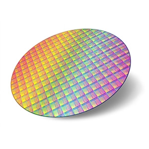
Main source: https://ganwafer.mystrikingly.com/
#epi wafer#epi wafer manufacturer#epi wafer supplier#epi wafer wholesale#epi services china#epi services
1 note
·
View note
Text
Silicon EPI Wafer Market: Global Industry Growth, Market Size, Market Share and Forecast 2020-2027
According to the recent report published by Research Corridor, the Global Silicon EPI Wafer Market is expected to provide sustainable growth opportunities during the forecast period from 2020 to 2027. This latest industry research study analyzes the Silicon EPI Wafer market by various product segments, applications, regions and countries while assessing regional performances of numerous leading market participants.
The report titled "Silicon EPI Wafer Market - Global Trends, Market Share, Industry Size, Growth, Opportunities, and Forecast - 2020 – 2027" offers a holistic view of the Silicon EPI Wafer industry encompassing numerous stakeholders including raw material suppliers, providers, distributors, consumers and government agencies, among others. Furthermore, the report includes detailed quantitative and qualitative analysis of the global Silicon EPI Wafer market considering market history, product development, regional dynamics, competitive landscape, and key success factors (KSFs) in the industry.
Browse Full report on Global Silicon EPI Wafer Market report at https://www.researchcorridor.com/silicon-epi-wafer-market/
The report includes a deep-dive analysis of key countries including the U.S., Canada, the U.K., Germany, France, China, Japan, India, Australia, Mexico, Brazil and South Africa, among others. Thereby, the report identifies unique growth opportunities across the world based on trends occurring in various developed and developing economies.
Silicon EPI Wafer Market report summarizes the positive growth rate in upcoming years, and market size with competitive analysis. Our experts have analyzed the historical data to compare with the current market scenario to calculate the market growth in the coming years. The study provides an exhaustive report that includes an executive summary, scope, and forecast of the market.
The Silicon EPI Wafer Market Segmentation:
By Type
Heteroepitaxy
Homoepitaxy
By Wafer Size
6-inch
8-inch
12-inch
Others
By Application
LED
Power Semiconductor
MEMS-based Devices
By Industry Vertical
Consumer Electronics
Automotive
Healthcare
Industrial
Others
By Region:
· North America
· Europe
· Asia Pacific
· Latin America
· Middle East & Africa
To know more about the study, make an inquiry before purchase @ https://www.researchcorridor.com/inquiry/?id=143929
List of Key companies:
Nichia Corporation
Applied Materials
Sumco Corporation
Epigan
ASM
Global Wafers
Siltronic
Wafer World Inc.
Key Questions Answered by Silicon EPI Wafer Market Report
Product popularity and adoption based on various country-level dynamics
Regional presence and product development for leading market participants
Market forecasts and trend analysis based on ongoing investments and economic growth in key countries
Competitive landscape based on revenue, product offerings, years of presence, number of employees and market concentration, among others
number of employees and market concentration, among others
To know more about this study, request a free sample report @ https://www.researchcorridor.com/request-sample/?id=143929
About Us:
Research Corridor is a global market research firm. Our insightful analysis is focused on developed and emerging markets. We identify trends and forecast markets with a view to aid businesses identify market opportunities optimize strategies. Our expert’s team of analysts’ provides enterprises with strategic insights. Research Corridor works to help enterprises grow through strategic insights and actionable solutions. Feel free to contact us for any report customization at [email protected] .
Media Contact:
Company Name: Research Corridor
Contact Person: Mr. Vijendra Singh
Email: [email protected]
Contact no: +91 989-368-5690
Visit us:
https://www.researchcorridor.com/
0 notes
Text
Chip Scale Package (CSP) LED Market Share, Trend, Segmentation and Forecast 2019
Chip Scale Package (CSP) LED Market Synopsis
Globally, the chip scale package LED Market is expected to grow from USD 743.8 million in 2018 to USD 1,807.5 million by 2023, at a CAGR of 19.4% during the forecast period, 2018–2023.
Chip scale package LED is an advancement over traditional LEDs where the packaging process includes attachment of a die with an interposer (ceramic substrate), resulting into a packaged LED. In the manufacturing process of a chip scale package LED, the packaging processes are avoided as the chip is singulated and coated using phosphor. Once the wafer is diced, a chip scale package LED becomes ready for use on a PCB. By eliminating many production processes, the manufacturing cost of chip scale LED is also much lesser than a traditional LED. This also reduces the chances of manufacturing defective products.
Get Sample of Chip Scale Package (CSP) LED Market Report @ https://www.marketresearchfuture.com/sample_request/7299
The major driving factors for the chip scale package LED market are low manufacturing cost, and high package density. The product is expected to witness a huge adoption in the automotive sector. The applications in general lighting is another big opportunity for the chip scale package LED market to grow with significant rate in the upcoming years. Limited applications of the chip scale package LEDs acts as a major restraining factor for the market. In the applications segment, the backlighting unit (BLU) is expected to dominate the market in terms of market size during the forecast size due to its high demand in electronic products, such as TV, monitor, and other display systems.
Chip Scale Package (CSP) LED Market Key players
The prominent players in Chip scale package LED market are Lumileds Holding B.V. (US), Samsung Electronics Co., Ltd. (South Korea), Semiconductor Co., Ltd. (South Korea), OSRAM Opto Semiconductors GmbH (Germany), LG Innotek (South Korea), Epistar Corp. (Taiwan), Cree, Inc. (US), Genesis Photonics Inc. (Taiwan), Semileds Corporation (Taiwan), and Lextar Electronics Corporation (Taiwan).
Chip Scale Package (CSP) LED Market Competitive Analysis
According to the latest trend in the chip scale package LED market, most enterprises are expanding their technological capabilities, with increased investments in research and developments activities. Most of the companies have adopted inorganic strategy to expand their businesses, wherein, partnership and collaboration accounted for XX%, whereas; merger & acquisition accounted for XX% of the overall key development undergone by the key players in the market.
Chip Scale Package (CSP) LED Market Segmentation.
The global chip scale package LED Market is segmented into application, power range, and region/country.
By application, the market is segmented into backlighting unit (BLU), general lighting, automotive lighting, flash lighting, and others.
By power range, the market is segmented into high power and low- and mid-power.
By region, the market is segmented into North America, Europe, Asia-Pacific, and rest of the world.
Chip Scale Package (CSP) LED Market Regional Analysis
The global market for chip scale package LED is estimated to grow at a significant rate during the forecast period from 2018 to 2023. The geographical analysis of global chip scale package LED market is studied for North America, Europe, Asia-Pacific, and rest of the world.
Asia Pacific is expected to dominate the chip scale package LED market during the forecast period. Asia Pacific region is considered as the most potential region in terms of development and adoption of chip scale package LEDs in the areas of smartphone and display systems. The region has a huge potential for revenue generation in the chip scale package LED market, particularly from consumer electronics industry verticals. China is expected to be the dominating country in the Chip scale package LED market in Asia Pacific region during the forecast period.
North America is expected to grow at the fastest rate during the forecast period. The region has presence of many innovative semiconductor companies that support in boosting growth of chip scale LED products in the region. US is the leading country in the North America region in terms of market share and this trend is expected to continue in the upcoming years.
Intended Audience
LED Foundaries
Wafer suppliers
EPI Houses
Display System Manufacturers
Semiconductor component suppliers
Standard Making Bodies and Associations
Venture Capitalists
Resellers and Distributors
Original Equipment Manufacturers/Original Device Manufacturers
End User Industries
About Market Research Future:
At Market Research Future (MRFR), we enable our customers to unravel the complexity of various industries through our Cooked Research Report (CRR), Half-Cooked Research Reports (HCRR), Raw Research Reports (3R), Continuous-Feed Research (CFR), and Market Research & Consulting Services.
Contact:
Market Research Future
+1 646 845 9312
Email: [email protected]
0 notes
Text
Europe Epitaxial (Epi) Wafer Market Sales Industry Research Report 2022
Marketresearchdata.net has added a new industry research report on Europe and Regional Epitaxial (Epi) Wafer Industry Production, Sales and Consumption Status and Prospects Professional Market Research Report. The report predicts the market size of Europe Epitaxial (Epi) Wafer Market is expected to reach XX billion by 2022.
Click below to request sample of the report:
https://www.marketresearchdata.net/Reports/make_sample_request/35282
This report focus on Europe and regional market, providing information on major players like manufacturers, suppliers, distributors, traders, customers, investors and etc., major types, major applications and etc. Data type include capacity, production, market share, price, revenue, cost, gross, gross margin, growth rate, consumption, import, export and etc. Industry chain, manufacturing process, cost structure, marketing channel are also analyzed in this report.
This report provides valuable information for companies like manufacturers, suppliers, distributors, traders, customers, investors and individuals who have interests in this industry.
Major companies are as follows:
Applied Materials
GlobalWafers
ASM International
EpiWorks
Jenoptik
Topsil Semiconductor Materials
SunEdison Semiconductor
Hitachi Kokusai Electric
Tokyo Electron
Nichia
Major classifications are as follows:
50mm to 100mm
100mm to 150mm
Above 150mm
Major applications are as follows:
Microelectronics Industry
Photovoltaics Industry
Photonics Industry
Major regions are as follows:
Germany
France
United Kingdom
Spain
Italy
Make an enquiry about this report:
https://www.marketresearchdata.net/Reports/make_enquiry_request/35282
Key Topics Covered:
Chapter 1 Industry Overview
Chapter 2 Production Market Analysis
Chapter 3 Sales Market Analysis
Chapter 4 Consumption Market Analysis
Chapter 5 Production, Sales and Consumption Market Comparison Analysis
Chapter 6 Major Manufacturers Production and Sales Market Comparison Analysis
Chapter 7 Major Classification Analysis
Chapter 8 Major Application Analysis
Chapter 9 Industry Chain Analysis
Chapter 10 Europe and Regional Market Forecast
Chapter 11 Major Manufacturers Analysis
Chapter 12 New Project Investment Feasibility Analysis
Chapter 13 Conclusions
Chapter 14 Appendix
To browse full report visit:
https://www.marketresearchdata.net/category/chemicals_materials/35282-europe-and-regional-epitaxial-epi-wafer
0 notes
Text
Overview on Epitaxy and its Applications
Epitaxy
Derived from the Greek word epi, which means above, and taxis which indicates an ordered manner. The LED Epi wafer is very reliable. This process forms one or several crystalline thin films that can be of the same or different chemical compositions and it has the structure as the substrate. In the technique of crystallography where natural or artificial crystals are grown on a crystalline substrate, Epitaxy is an important technique that is used.
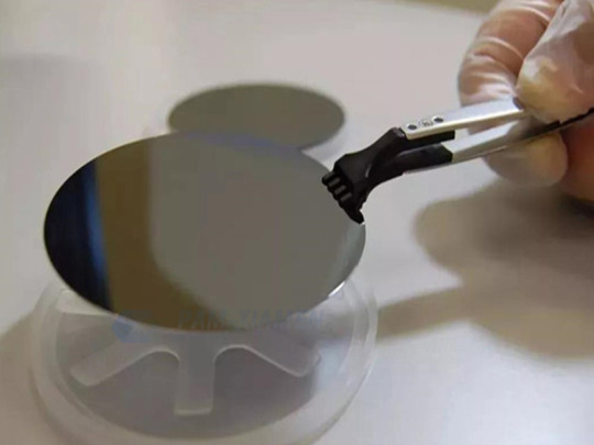
In nanotechnology and semiconductor fabrication the process is used where it is of commercial importance. Epitaxy is the only affordable method for many semiconductor materials where high-quality crystals are growing. It marks little importance for most thin-film applications, for example, hard or soft coatings, or optical coatings whereas in semiconductor thin-film technology it is critical. In this in electronic and photonic devices such as computer video displays and telecommunication applications, the growth of semiconductor materials forms layers and quantum wells. For maximum technological applications, the desire is for the deposited material to form a crystalline film that concerning the substrate crystal structure has one well-defined orientation. You can purchase wafers from LED Epi wafer supplier.
Applications and Epitaxial Growth of Thin Film Materials
In electronics, optoelectronic and magneto-optics epitaxial growth of thin-film materials has numerous applications. In several ways, growth can occur where the most common is the vapor phase epitaxy (a modification of chemical vapor deposition), where from vapor the atoms for deposition on the substrate are taken and growth occurs at the gaseous/solid interface. On the substrate, solid-phase epitaxy deposits a thin non-crystalline film which is then heated to form a crystalline layer, while in the liquid phase from a liquid source the layers grown in epitaxy are observed.
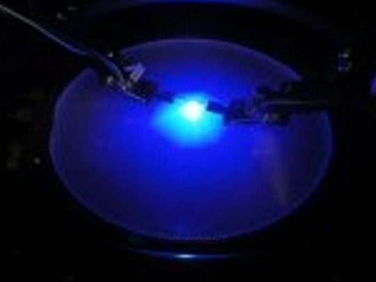
In producing device quality layers the latter is by far the cheapest and easiest route, but in terms of using metal-organic chemical vapor deposition (MOCVD) and molecular beam epitaxy (MBE) is growing. MOCVD and MBE are more versatile but the Initial costs are expensive and with atomic-layer control, it can readily produce multilayer structures, which is basic to Nanoengineering. The LED Epi wafer manufacturer is opted by many.
14 notes
·
View notes
Text
Use of Wafer Front End in the Semiconductor Manufacturing Process
When the process of front-end production is completed then to save the chip the wafers are transmitted to the assembly facility. It brings the heat from the devices, assists the integration into the electronic systems, and confines the electric interference.
Building of wafers
In manufacturing, the semiconductor has an essential role no matter whether it is a small chip or a big motor car. In semiconductor production, the processing of chemical elements is done in the wafer form. Within the plastic cassettes, the LED Epi wafer is built up and with the specific production time, the circumstances are made out of steps.
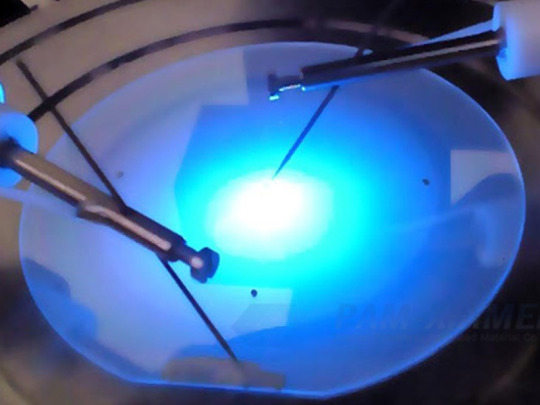
Wafer handling equipment is the emerging manufacturing process that is made to check the cleanliness and environmental control. Within the semiconductor front-end industry, it has diminished from the semiconductor devices manufacturing. For the significant environments, the process is carried out where certain factors are checked out, such as humidity, particle contamination, temperature, and controlled with the particular parameters.
To handle delicate thin wafers the bonding of the device wafer is done with a rigid carrier substrate before the back-thinning process. With the use of an adhesive bonding layer, the originally thick device wafer is bonded with its active surface to a carrier wafer.
It arrives in a consignment production form if we discuss the semiconductor backend production that is based on many customers' various orders. Picked up from the GaN LED wafers conveyed from the front-end production, the backend companies with the non-defective dies start building the final product in such a case. It makes the products reach their place within the due dates.

LED epitaxial wafer gives a detailed description of the non-repairable chips that are pushed to the next step. The defectiveness and the opposed information are filled up when this test gets completed and based on the matter it is passed through the backend process. The information conveys that only non-defective dies are taken in the final product. Wafer handling equipment is the emerging manufacturing process that is made to check the cleanliness and environmental control. Within the semiconductor front-end industry, it has diminished from the semiconductor devices manufacturing. The manufacturers, as with the bump in the semiconductor's request, turn on a further note towards automating the production process.
Original source: https://ganwafer.weeblysite.com/
3 notes
·
View notes
Text
SAPPHIRE WAFERS / SAPPHIRE SUBSTRATES
https://www.cryscor.com/products/sapphire-wafers-sapphire-substrates/

Due to the less mismatched lattice and stable chemical and physical properties, sapphire(Al2O3) wafer is the popular substrates for III-V nitrides, superconductor and magnetic epi-film. They are widely used in GaN and thin-film epitaxial growth, silicon on sapphire, LED market and optics industry.
CRYSCORE is a professional sapphire wafer supplier who manufactures 99.999% high purity single crystal polished sapphire wafers for epitaxy. And our sapphire (Al2O3) substrates feature excellent surface finish, which is the key LED parameter.
If you are looking for reliable sapphire wafer suppliers, contact us now.
FEATURES OF SINGLE CRYSTAL SAPPHIRE
1. Sapphire has a high optical transmittance, so it is widely used as microelectronic tube dielectric material, ultrasonic conduction element, waveguide laser cavity and other optical elements, as window materials for infrared military devices, space vehicles, high-intensity lasers and optical communications...
2. Sapphire has high rigidity, high strength, high working temperature, abrasion resistance, corrosion resistance characteristics, so it is often used in harsh environments, such as boiler water gauge (high-temperature resistance), commodity bar code scanner, bearing and other precision manufacturing (wear resistance), coal, gas, well detection sensors and detector windows (anti-corrosion)...
3. Sapphire has the characteristics of electrical insulation, transparency, good thermal conductivity and high rigidity, so it can be used as the substrate material of integrated circuits, such as LED and microelectronic circuits, ultra-high-speed integrated circuit.
CRYSCORE'S EXCELLENT SAPPHIRE WAFERS
99.999 % high purity single crystal Al2O3 material.
Special CMP (Chemical Mechanical Polishing) technology to ensure its performance at a low cost.
Excellent surface quality in all orientations (less than 0.2 nm for C-plane, less than 0.5 nm for A-plane, M-plane, R-plane, N-plane, V-plane, 10-14, etc.)
Cleaned in class 100 cleanroom by ultrapure water with quality above 18MΩ *cm.
25 pcs a pack or single pack is available to maximize customer flexibility in their research.
Traceable product serial number.
Compact carton packaging for safer shipping and cost-saving.
Standard wafers are Generally in stock to ensure a quick delivery.
LOOK AT WHERE SAPPHIRE WAFER APPLIED
1. Semiconductor LED industry (MOCVD epitaxial GaN substrate)
In general, C-plane sapphire is needed in this area. R-plane or M-plane mainly used to grow non-polar/semi-polar plane epitaxial layers to improve the luminescence efficiency.
2. The growth of III-V or II-VI compound semiconductor.
3. Microelectronic IC applications especially Very High-Speed Integrated Circuit, SOS
Generally, it is a silicon heteroepitaxial deposition on R-plane sapphire.
4. Hybrid microelectronics
Hybrid microelectronics products are mainly HIC and MCM. It has high requirements on the substrate, while sapphire's characteristics such as stable dielectric constant and low dielectric loss make sapphire wafer the most commonly used substrate for HIC and the main substrate for MCM. Generally, the A-plane sapphire wafer is needed.
SAPPHIRE WAFER PROCESSING
At the very beginning, we have a crystal boule.
Crystal growing: Produce high-quality sapphire monocrystals via furnace.
Sapphire ingot processing: Drill out the ingot, Ground the ingot, Quality inspection.
Then we get the sapphire ingot.
Orientation: Position the ingot on the sawing machine.
Sawing: Cut the ingot into thin wafers.
Lapping: Lap the wafer to remove the scratched layer and improve its flatness.
Chamfer: Trim the edge of the wafer into an arc to improve the mechanical strength, to avoiding stress concentration.
Polishing: Reduce the surface roughness to reach the epitaxial wafer grade.
Cleaning: Remove dirt from the wafer surface.
Quality inspection: Inspect wafer with a high precision instrument to meet customer's requests.
Finally, we get the sapphire wafer.
0 notes
Last Seen Blogs

limbel
okay

cosmosmoderndentalelmhurst
Cosmos Modern Dental - Elmhurst

shobag
Call me Ho Bagg

codehunter
Codehunter

makchopi
MANHWA SPOILERS