#fab automation
Explore tagged Tumblr posts
Visit Tumblr Blog
Explore Tumblr blogs with no restrictions, modern design and the best experience.
Last Seen Tumblr Blogs


Fun Fact
1,644 Tumblr posts in 1 second.
Text
SECS/GEM on JEOL JWS-7515 Metrology Equipment: Enhancing Efficiency with EIGEMBox
In the fast-paced world of semiconductor manufacturing, precision and efficiency are paramount. One key aspect of this process is the metrology equipment used to ensure that every component meets stringent quality standards. The JEOL JWS-7515 is a leading tool in this field, particularly when combined with the EIGEMBox, which facilitates the SECS/GEM protocol. In this blog, we’ll explore the significance of SECS/GEM, the features of the JEOL JWS-7515, and how the EIGEMBox enhances metrology processes.
What is SECS/GEM?
SECS/GEM stands for SEMI Equipment Communication Standard/Generic Equipment Model. It is a widely adopted communication protocol in the semiconductor manufacturing industry that allows for seamless data exchange between manufacturing equipment and host systems. This standard is critical for achieving automation and real-time data acquisition, which helps improve production efficiency and reduce errors.
Why SECS/GEM Matters
Standardization: By providing a uniform communication protocol, SECS/GEM simplifies the integration of various equipment and systems, leading to smoother operations.
Real-time Monitoring: With SECS/GEM, manufacturers can monitor equipment performance in real-time, allowing for quick adjustments and better decision-making.
Data Collection: The protocol facilitates extensive data collection, which is essential for analysis, reporting, and continuous improvement initiatives.

Overview of JEOL JWS-7515
The JEOL JWS-7515 is an advanced metrology tool designed for high-resolution imaging and analysis of semiconductor wafers. Here are some of its standout features:
High-Resolution Imaging
The JWS-7515 utilizes cutting-edge electron beam technology to achieve high-resolution imaging. This capability allows for detailed inspections of wafer surfaces, crucial for identifying defects that could compromise performance.
Versatility
This equipment is versatile enough to handle various materials and applications, making it an invaluable asset in a semiconductor fab. Its ability to analyze different substrates and feature sizes helps manufacturers maintain high standards across diverse product lines.
Automated Functionality
Automation is a key feature of the JWS-7515, which enhances throughput and minimizes human error. The system’s ability to integrate with software tools and other equipment makes it a central hub for metrology operations.
The Role of EIGEMBox
The EIGEMBox is a powerful tool that enhances the capabilities of the JEOL JWS-7515 by facilitating SECS/GEM communication. Here’s how it works:
Seamless Integration
The EIGEMBox acts as a bridge between the JEOL JWS-7515 and the host system, enabling seamless data transfer. This integration is crucial for manufacturers who require real-time insights into their metrology processes.
Enhanced Data Management
With the EIGEMBox, data collected by the JWS-7515 can be efficiently managed and analyzed. The ability to centralize data from multiple sources helps manufacturers streamline operations and improve decision-making.
Flexibility and Scalability
The EIGEMBox is designed to be flexible, accommodating a variety of equipment and systems. As manufacturing needs evolve, the EIGEMBox can be scaled to meet increased demands without significant infrastructure changes.
Benefits of Using SECS/GEM with JEOL JWS-7515 and EIGEMBox
Improved Efficiency
By automating data exchange and analysis, the combination of SECS/GEM, the JEOL JWS-7515, and the EIGEMBox significantly improves operational efficiency. Manufacturers can reduce downtime and optimize workflow, leading to faster production cycles.
Enhanced Quality Control
The ability to conduct real-time monitoring and analysis of wafer conditions ensures that quality control measures are always in place. This capability minimizes the risk of defects reaching the production stage, ultimately enhancing product reliability.
Data-Driven Decision Making
Access to comprehensive, real-time data allows manufacturers to make informed decisions quickly. This responsiveness is critical in a competitive landscape where even minor delays can have significant consequences.
Implementation Considerations
While the benefits of integrating SECS/GEM with the JEOL JWS-7515 and EIGEMBox are clear, several implementation considerations should be taken into account:
Training and Support
To fully leverage the capabilities of these technologies, manufacturers should invest in training for their staff. Understanding how to use the equipment and interpret data is essential for maximizing the benefits.
System Compatibility
Ensuring that the EIGEMBox is compatible with existing systems is crucial for a successful integration. Manufacturers should conduct thorough assessments before implementation to identify any potential challenges.
Ongoing Maintenance
Regular maintenance of both the JWS-7515 and the EIGEMBox is essential to maintain optimal performance. A proactive maintenance schedule can help prevent equipment failures and ensure long-term reliability.
Conclusion: Elevate Your Metrology Operations Today
The integration of SECS/GEM with the JEOL JWS-7515 metrology equipment, enhanced by the EIGEMBox, represents a significant advancement in semiconductor manufacturing. By improving efficiency, enhancing quality control, and enabling data-driven decision-making, this combination positions manufacturers for success in a highly competitive market.
If you're looking to elevate your metrology operations and embrace the future of semiconductor manufacturing, now is the time to act! Contact us today to learn more about how SECS/GEM, JEOL JWS-7515, and EIGEMBox can transform your processes. Don’t miss out on the opportunity to enhance your operational efficiency and product quality!
#secs/gem#fab automation#equipment software#secs/gem software#eigembox#secs/gem protocol#semiconductor#secs gem software#JEOL JWS-7515#Metrology Equipment
1 note
·
View note
Text

Photo by Arnold Newman.
“[W]e built a little studio at home to save the drive up and down the M4. And the studio is really very nice — little plug for Eddie Veale of Audiotech because he did a fantastic job and it sounds really nice. You know, because most home studios have a lot of trouble, you know. And it’s not really practical in some cases for people to have a home studio.” - George Harrison, Capital Radio, 1974 “Of all the former ‘Fabs,’ to use his customary term, George Harrison has remained the greatest creative homebody. […] George has rolled out of bed and returned again and again to Friar Park Studios, Henley-on-Thames (or F.P.S.H.O.T., for short) to tinker, compose and do his formal recording. […] Besides 'Cloud Nine,’ George recorded the 'Dark Horse,’ '33 1/3’ and 'George Harrison’ albums in his F.P.S.H.O.T. atelier, located in what was formerly a ballroom of the house. 'The studio was installed round 1971 and there’s been a few updates, cause when I originally put the studio in it was a 16-track. In terms of the monitoring system, after all those years in the Abbey Road EMI Studios, I put in Altec speakers. My experience in Abbey Road was that whenever the Beatles worked there and we thought we had a great sound, we’d play it back on the Altecs and it sounded terrible — ordinary. So they’re very boring in a way — and this must sound strange — but they’re also accurate! See, the Altecs don’t flatter the sound; it’s not easy to get good bass and drum sounds with them. But when I built my studio I didn’t want hype. I wanted what I’m hearing to be what it is. That way, when you play it back anyplace else it sounds fantastic! […] I’ve since made F.P.S.H.O.T. into a 24-track board. […] I’m going to get a few different choice modules made soon, but I don’t really want to go for a brand new SSL board and all that. Automation is nice in some respects, but I got my first skills at Abbey Road, so I prefer the old components, and spending a friendly weekend getting the manual mix you want. Just as I much prefer my ancient Fender Strat.’” - Musician, November 1987 (x)
#George Harrison#quote#quotes by George#quotes about George#FPSHOT#Friar Park#1970s#Harrison songwriting#Harrisongs#fits queue like a glove
61 notes
·
View notes
Text
Fuckin
Semi masturbatory caffeinated ramble reflecting on skills acquired in my PhD
Thinking about how broad and interdisciplinary my project is and the kinda of things I have to be familiar with or an expert in. I get down on myself sometimes for progress but looking at all the shit I've learned.... Without formal classes or a senior grad student or (for the majority of it) no post doc. And a PI who can't help bc she's really a business lady at this point not a professor. Maybe shouldn't be hard on myself?
Like. I did completely different projects in undergrad (biotech/proteins/genetics/regenerative medicine, advanced manufacturing/composite fabrication/CNC/welding/process statistics, translational neuropharma studies of addiction/rodent handling and operant training and behavioral video analysis/neural tissue slicing n staining/hand making neuroelectrodes for implantation, design and fabrication of impedance spectroscopy based electrochemical sensors/automation of sensor fab and use w a micro fluidic flow cell)
Like. Since I've started I've learned:
- how to do multi-step air-free water-free chemical synthesis (with glove box and schlenk line) and purification (extraction, filtration, chromatography) of light sensitive amphiphiles (extra tricky)
- how to get and read NMR even for massive fucking molecules and interpret weird peaks (I can casually see if I've got water or any of my common solvents contaminating the spectra without referencing a table at this point)
-how to fucking take down and set up and fix everything in our chemical synthesis lab (because we moved and all our shit was abused for years) and all the intricate non-unified and sometimes conflicting rules for hazardous chemical storage
- the theory/math and how to actually use the equipment to do optoelectronic/photophysical characterization (e.g. using the UV vis spectrometer and writing python to convert the data files into readable tables and figures, learning theory so I can develop equations to relate photon flux to change in absorbance of an actinometer ((light sensitive molecule with a consistent quantum yield)) then obtain quantum yield of charge transfer in a different molecule but same setup, how to use the fluorimeter and get intensity and quantum yield, how to set up lasers and LEDs, what cuvettes to use, how to get fluorescence lifetimes or take two photon excitation data, how to spin coat wafers n do thin film transistor studies), more theory about how photo induced electron transfer voltage sensors work and the importance of angle of insertion on sensitivity (and how to measure it with polarization microscopy) other voltage sensing dye mechanisms like FRET or electrochromic dyes and why to use intensity vs lifetime vs whatever when interpreting signal readouts and the extrinsic and intrinsic factors affecting that interpretation.
- how to do vesicle fabrication and immobilize for imaging, typical membrane compositions and dynamics (e.g. phase orders depending on cholesterol concentrations, significance of packing parameters to membrane organization), measurimg particle radius with DLS, controlling inner cargo and gradients over a membrane by manipulating the bulk solution, the interplay between non radiative decay and the stiffness of the membrane microenvironment around a fluorophore
- the math and bio behind electrophysiology/advanced neuroscience pertaining to modeling and calculating and quantifying signalling/equivalent RC circuit analysis, what spatiotemporal requirements there are for studying this shit <- though this was through a class, not self taught
- I already had cell culture experience and did some adherent and suspended cultures, some live dead imaging assays, etc, but I've learned new facets like how to go about picking electrically exciteable lines (ease of growing? What media requirements? time to multiply and differentiate? What agent to differentiate? How to induce firing without a patch clamp?) and troubleshooting uptake/optimizing staining and imaging parameters (what media or buffer for growth vs staining vs washing vs imaging? Can it have serum? Can it have calcium and magnesium? What salts, how is it buffered, whats the osmolarity I can get away with? What concentrations work for what # of cells? What dilution factors? Do I need to admix equivolumes of dye solution and cell solution? Do I prep the organic solvent+ dye + aqueous solution with sonication or filtration or vortexing before mixing? Is DMSO or ethanol or DMF a better organic for dispersal or biocompatibility? What's the Ideal incubation time for uptake and viability? How long before I absolutely need to image or the dye gets internalized? If it's retained long, how many days could I image for?) for my tricky aggregation-prone non-diffusive thermodynamically-partitioned dye. Also stuff like what commercially available live imaging dyes can I compare to or complement my visualizations with or use for colocalization studies (other lipophilic membrane dyes that insert in the bilayer with preferences for diff order regions? What about comparison with surface adhering dyes like WGA-iFluor that bind surface sugars, to show that our dye can laterally diffuse to areas blocked by cell-cell contacts?), what fluorescence specific parameters do I need to characterize (photo toxicity/photo bleaching time?)
And then there's other shit I've picked up like. Idk. How to make orders in the particular institute I'm in. Better citation managers and ways to search literature. Recognizing what groups and journals and conferences are major players in the fields I'm touching. Getting comfy presenting my shit.
I need to learn a little more about microscopy (especially FLIM and how to build a polarizer module into the scope we have for polarization microscopy), and a little more about the state of the art for voltage dyes and live-imaging dye characterization but man. I think I'm getting somewhere. I'm starting to know enough to see the end of this project and pick my directions moving forward and argue when my PI is wrong
Gahhhhhh
#i should not drink coffee and then go to the bathroom on my phone or you get sloppy brain dumps like this#blog#stem#academia
4 notes
·
View notes
Text
0 notes
Text
🛠️ Revamp Your Dubai Home: Couch Repair, Fitted Wardrobes & Stylish Bedroom Curtains
Transforming your home in Dubai doesn't simply mean purchasing new goods, you may want to also breathe new life into your existing possessions and optimize your efficiency. Whether it's revamping a favorite couch, having custom wardrobes installed, or simply refreshing your bedroom with beautiful curtains, the right services can absolutely increase comfort, function and style. Here is how to update your home with the essential upgrades.
🪑 Couch Repair Services in Dubai: Bring Your Sofa Back to Life
Why Couch Repair?
Your sofa is often the centerpiece of your living room, supporting countless moments of relaxation and entertainment. Rather than replacing it, repair services offer:
Cost-effective solutions—upholstery repairs cost far less than new furniture.
Sustainability benefits—repairing reduces waste and environmental impact.
Preserving sentimental value—retain comfort and familiarity while refreshing the look.
Common Couch Repairs
Frame repairs: Fixing loose joints, broken rails, or structural sag.
Spring and cushion restoration: Replacing worn coils or foam for support.
Reupholstery: Updating fabric with new, durable material.
Stain removal and cleaning: Professional deep-cleaning for hygiene and freshness.
What to Look For
Experienced technicians with before/after portfolios.
Quality materials like hardwood frames and high-density foams.
Optional upgrades—stain-resistant fabrics or enhanced cushioning.
Warranty on both labor and materials.
Efficient timeline—some repairs completed within a few days.
🧱 Fitted Wardrobe Design Dubai: Tailored Storage for Every Home
Benefits of Fitted Wardrobes
Fitted wardrobes make the most of your bedroom’s space, offering:
Personalized dimensions: Ideal fit even in awkward nooks or sloped ceilings.
Customized organization: Sections for clothes, shoes, accessories, and more.
Premium aesthetics: Integrated design that complements your décor.
Long-term value: Higher appeal for resale and rental interest.
Design Features to Consider
Door types: Choose from sliding, hinged, bi-fold, or pocket doors.
Material choices: MDF with veneer, high-gloss laminate, or natural wood finishes.
Internal layout: Adjustable shelves, pull-out drawers, valet rods, and shoe racks.
Lighting options: LED strips under shelves or motion-activated lights.
Accessory add-ons: Full-length mirrors, tie racks, and premium handles.
The Design Process
Consultation & measurement
Design proposal with 3D renderings
Material selection
On-site installation by carpentry experts
Final inspection and handover
🛏️ Bedroom Curtains in Dubai: Elegant Window Dressing & Comfort
Dubai Furniture Company offers a comprehensive range of bedroom curtains, including custom, sheer, blackout, and cotton options—ideal for privacy, insulation, and decorative style .
What Makes Their Curtains Stand Out?
Blackout curtains for optimal sleep quality and darkness .
Cotton curtains are valued for their durability and ease of maintenance.
Sheer curtains that provide gentle light while maintaining privacy.
Bespoke designs tailored to your bedroom's aesthetic and dimensions.
Competitive pricing with professional installation options.
Choosing the Right Curtains
Blackout: Ideal for night workers or light-sensitive sleepers—block light and reduce noise.
Thermal/Cotton: Excellent for Dubai’s climate—balancing warmth and ventilation.
Sheer + blackout layering: Flexibility in light control and style.
Eyelet (grommet), pinch-pleat, or rod-pocket styles to match your décor.
Proper installation: Rod bracket placement above the window frame enhances height perception.
Professional Installation Tips
Ensure accurate measurement—curtains should be 1.5–2× window width and typically touch or slightly pool the floor.
Opt for motorized systems when convenience and automation are desired.
Choose high-quality rods and finials for durability and visual consistency.
Request and inspect fabric samples before finalizing.
🌟 Integrating All Three Services for a Cohesive Home Upgrade
Step 1: Audit What You Have
Identify sofas with signs of wear, cramped closets, and outdated curtains. Rank them by urgency and impact.
Step 2: Plan Your Budget & Timeline
Balance each component—couch repairs might cost AED 500–1,500+, fitted wardrobes AED 2,000–10,000+, curtains AED 300–2,000+. Obtain multiple quotes and bundle services where possible.
Step 3: Harmonize Design & Materials
Recovered sofas should complement the wardrobe finishes and curtain fabrics.
Choose colors that tie together���warm neutrals, rich wood tones, or bold contrasts.
Step 4: Schedule Efficiently
Start with couch repair, then wardrobe installation, then curtain fitting. This prevents damage and ensures seamless completion.
🏠 Real-Life Makeover Example
Villa in Al Barsha:
Sofa reupholstered with premium linen-look fabric.
Fitted wardrobe in white gloss laminate with integrated lights and mirrors.
Layered blackout and sheer curtains in pale grey.
Results:
Sofa rejuvenated at 30% of replacement cost.
Bedroom visually expanded, well-organized, and clutter-free.
Enhanced ambiance, thermal comfort, and sleep quality with curtains.
Why Choose Local Dubai Specialists?
Expertise in Gulf climate: Materials suited for heat and humidity.
Custom solutions: Tailored service ensures perfect fit and harmonious design.
End-to-end service: From design consultation to aftercare support.
Warranty & Guarantee: Peace of mind with backed workmanship.
✅ Final Tips Before You Begin
Task
Recommendation
Inspect furniture
Address worn frames or fabrics early
Measure precisely
For wardrobes & curtains, accuracy matters
Request samples
Test fabric, laminate, or upholstery colors
Bundle installations
Cost-saving and cohesive outcomes
Quality service
Prioritize providers with verified reviews & portfolios
Let the Dubai Furniture Company Elevate Your Home
From sofa restoration to fitted wardrobe craftsmanship and luxurious bedroom curtains, these upgrades revitalize spaces aesthetically and functionally. Reach out to Dubai Furniture Company today for personalized consultations, expert installation, and a refreshed, comfortable living environment.
0 notes
Text
Transforming Semiconductor Manufacturing Using Intelligent Industrial Control Systems

Semiconductors are the foundation of today’s technology, enabling the operation of devices ranging from smartphones to cutting-edge AI systems. As global demand for high-performance chips surges, chipmakers are under increasing pressure to scale production and innovate rapidly. Here is where Smart manufacturing comes into the picture.
Smart manufacturing is revolutionizing the semiconductor industry by introducing advanced, data-driven production methods. By integrating automation, artificial intelligence (AI), machine learning (ML), and the Internet of Things (IoT), manufacturers are unlocking new levels of precision, responsiveness, and operational efficiency. Far from being just a trend, this shift is crucial for staying competitive in a rapidly evolving tech landscape.
With real-time data analytics and digitally connected systems, chip production is becoming quicker, more adaptable, and more cost-effective. It marks an essential shift in how semiconductors are designed, fabricated, and delivered to meet the demands of the digital age.
The convergence of automation, data intelligence, and digital control is quite essential. Nowhere is this more evident than in semiconductor manufacturing, where nanometer-level precision, speed, and scalability define success. At the heart of this transformation lies intelligent industrial control systems, a new breed of interconnected, adaptive, and data-rich control technologies that redefine how industrial operations are monitored and optimized.
As the demand for high-performance chips accelerates, semiconductor manufacturers are under immense pressure to boost production and maintain precision. Smart manufacturing is emerging as a game-changer, and at its core are Intelligent Industrial Control Systems (IICS) — blending automation, AI, and real-time analytics to create smarter, faster, and more reliable semiconductor fabs.
Smart Manufacturing: A Strategic Shift Traditional manufacturing can no longer meet the complexity and scale required by today’s semiconductors. Smart factories leverage systems like Distributed Control Systems (DCS), SCADA, and Programmable Logic Controllers (PLCs), layered with Advanced Process Control (APC) and IoT-enabled sensors. These allow for predictive maintenance, energy-efficient processes, and real-time quality control.
Why Intelligent Control Systems Matter In chip production, even a micron-level deviation can lead to massive losses. Intelligent control systems dynamically adjust variables, reducing downtime and waste. Leading companies like TSMC and Intel are already adopting these systems to optimize yield and time to market.
Key Benefits
Higher Yield: AI-powered APC reduces variability
Faster Time to Market: Real-time data boosts production speed
Energy Efficiency: Smart power supplies reduce operational costs
Predictive Maintenance: IoT sensors detect faults early
Compliance: SCADA systems offer traceability for audits
Real-World Impact A Singapore-based fab achieved a 15% reduction in scrap rates and 11% improvement in uptime within 6 months of integrating IICS.
Conclusion: To remain competitive in the age of AI, EVs, and 5G, semiconductor companies must embrace intelligent manufacturing. ACL Digital provides scalable, secure industrial control solutions that drive ROI and future-readiness.
As semiconductor demand surges, driven by AI chips, electric vehicles (EVs), and 5G infrastructure, manufacturers can no longer afford to rely on legacy systems. Intelligent industrial control systems offer not only automation but also adaptability, resilience, and a platform for continuous innovation. Smart manufacturing in semiconductors isn’t just about machines but about making better decisions faster. And that’s only possible when your control systems are as advanced as the products you’re building.
Ready to upgrade your fab with intelligent automation?
Contact us at [email protected] to explore how we can enhance your workplace transformation.
This blog was originally published on the website www.acldigital.com
0 notes
Text
Global High Voltage Power Supply for Electrostatic Chuck Market
High Voltage Power Supply for Electrostatic Chuck Market Analysis:
The global High Voltage Power Supply for Electrostatic Chuck Market size was valued at US$ 280 million in 2024 and is projected to reach US$ 485 million by 2032, at a CAGR of 8.1% during the forecast period 2025-2032
High Voltage Power Supply for Electrostatic Chuck Market Overview
This report provides a deep insight into the global High Voltage Power Supply for Electrostatic Chuck market covering all its essential aspects. This ranges from a macro overview of the market to micro details of the market size, competitive landscape, development trend, niche market, key market drivers and challenges, SWOT analysis, value chain analysis, etc. The analysis helps the reader to shape the competition within the industries and strategies for the competitive environment to enhance the potential profit. Furthermore, it provides a simple framework for evaluating and accessing the position of the business organization. The report structure also focuses on the competitive landscape of the Global High Voltage Power Supply for Electrostatic Chuck Market, this report introduces in detail the market share, market performance, product situation, operation situation, etc. of the main players, which helps the readers in the industry to identify the main competitors and deeply understand the competition pattern of the market. In a word, this report is a must-read for industry players, investors, researchers, consultants, business strategists, and all those who have any kind of stake or are planning to foray into the High Voltage Power Supply for Electrostatic Chuck market in any manner.
High Voltage Power Supply for Electrostatic Chuck Key Market Trends :
Rising Semiconductor Demand The growing demand for semiconductors in consumer electronics and automotive sectors is boosting the need for reliable electrostatic chuck power supplies.
Miniaturization of Electronic Components As electronic devices become smaller and more complex, precision in wafer handling is critical, driving demand for high-performance HV power supplies.
Adoption of Smart Manufacturing Semiconductor fabs are rapidly adopting smart manufacturing practices, fueling the demand for advanced and automated power supply systems.
Increasing Display Panel Production The expanding display industry, especially OLED and micro-LEDs, is creating new application avenues for HV power supplies in electrostatic chucks.
Focus on Energy Efficiency Manufacturers are investing in energy-efficient and compact power supply designs to reduce operational costs and footprint.
High Voltage Power Supply for Electrostatic Chuck Market Regional Analysis :
North America:Strong demand driven by EVs, 5G infrastructure, and renewable energy, with the U.S. leading the market.
Europe:Growth fueled by automotive electrification, renewable energy, and strong regulatory support, with Germany as a key player.
Asia-Pacific:Dominates the market due to large-scale manufacturing in China and Japan, with growing demand from EVs, 5G, and semiconductors.
South America:Emerging market, driven by renewable energy and EV adoption, with Brazil leading growth.
Middle East & Africa:Gradual growth, mainly due to investments in renewable energy and EV infrastructure, with Saudi Arabia and UAE as key contributors.
High Voltage Power Supply for Electrostatic Chuck Market Segmentation :
The research report includes specific segments by region (country), manufacturers, Type, and Application. Market segmentation creates subsets of a market based on product type, end-user or application, Geographic, and other factors. By understanding the market segments, the decision-maker can leverage this targeting in the product, sales, and marketing strategies. Market segments can power your product development cycles by informing how you create product offerings for different segments. Key Company
Creative Technology Corporation
Matsusada Precision Inc.
Advanced Energy
P.R.A. Co.,Ltd.
XP Power
PSTEK
Gripping Power, Inc.
Spellman
Hung Hui Technology
Market Segmentation (by Type)
Benchtop Type
Rack Mount Type
Module Type
Market Segmentation (by Application)
Semiconductor Process
Display Process
Market Drivers
Booming Semiconductor Industry The continuous growth in semiconductor device production is directly increasing the use of electrostatic chucks in wafer processing, driving market growth.
Growing Demand for Advanced Display Panels With increasing investments in high-end displays and flexible screens, the display process application is witnessing significant uptake.
Technological Advancements in HV Power Supplies Innovations like precise voltage control, remote monitoring, and miniaturized designs are making HV power supplies more efficient and desirable.
Market Restraints
High Cost of Advanced Systems The initial investment for high-end, precision HV power supplies remains a barrier for small-scale fabs and new entrants.
Complexity in Integration and Maintenance Installing and maintaining high voltage systems require technical expertise and regular calibration, which can slow adoption.
Limited Awareness in Emerging Markets Developing regions often lack awareness and infrastructure to adopt advanced electrostatic chuck systems, limiting market penetration.
Market Opportunities
Expansion in Asia-Pacific Semiconductor Hubs Countries like China, South Korea, and Taiwan are investing heavily in semiconductor fabs, opening massive growth opportunities.
Collaborations with Display Manufacturers Partnerships between HV power supply providers and display panel producers can accelerate innovation and adoption.
Eco-Friendly and Compact Designs R&D focused on sustainable, energy-efficient, and compact solutions can attract new customers and meet regulatory standards.
Market Challenges
Volatile Raw Material Prices Fluctuations in raw material costs affect the pricing and profitability of HV power supply systems.
Intense Market Competition Global and regional players compete aggressively, pushing prices down and pressuring margins.
Regulatory and Safety Standards Meeting international safety and quality certifications can delay product launches and increase compliance costs.
Key Benefits of This Market Research:
Industry drivers, restraints, and opportunities covered in the study
Neutral perspective on the market performance
Recent industry trends and developments
Competitive landscape & strategies of key players
Potential & niche segments and regions exhibiting promising growth covered
Historical, current, and projected market size, in terms of value
In-depth analysis of the High Voltage Power Supply for Electrostatic Chuck Market
Overview of the regional outlook of the High Voltage Power Supply for Electrostatic Chuck Market:
Key Reasons to Buy this Report:
Access to date statistics compiled by our researchers. These provide you with historical and forecast data, which is analyzed to tell you why your market is set to change
This enables you to anticipate market changes to remain ahead of your competitors
You will be able to copy data from the Excel spreadsheet straight into your marketing plans, business presentations, or other strategic documents
The concise analysis, clear graph, and table format will enable you to pinpoint the information you require quickly
Provision of market value (USD Billion) data for each segment and sub-segment
Indicates the region and segment that is expected to witness the fastest growth as well as to dominate the market
Analysis by geography highlighting the consumption of the product/service in the region as well as indicating the factors that are affecting the market within each region
Provides insight into the market through Value Chain
Market dynamics scenario, along with growth opportunities of the market in the years to come
6-month post-sales analyst support
Related Reports:

0 notes
Text
The Silent Enabler: How IC Substrates Power the Semiconductor Revolution
Breaking Down the IC Substrate Ecosystem
The global IC substrate market has transformed into a $14.6 billion industry (Yole Développement 2025), driven by three core technology segments:

Advanced Packaging Platforms
2.5D/3D IC substrates now enable 12-layer interposers with <1μm alignment precision
Fan-out wafer-level packaging (FOWLP) achieves 0.8μm line/space resolution
Heterogeneous integration substrates support 10+ chiplet configurations
Material Science Breakthroughs
Low-loss dielectrics (Dk<3.0 @ 100GHz) from 8 major chemical suppliers
Nanocomposite thermal interface materials with 15W/mK conductivity
Photosensitive dielectric films enabling 2μm laser patterning
Cutting-Edge Manufacturing Innovations
Leading manufacturers have deployed:
AI-Optimized Production
Neural networks reducing warpage by 40% through real-time parameter adjustment
Digital twin systems predicting yield with 98.7% accuracy
Automated optical inspection achieving 50 defects per billion opportunities
Sustainable Manufacturing
Closed-loop chemical recycling recovering 92% of process materials
Plasma treatment replacing chemical desmear in 35% of facilities
Waterless cleaning systems reducing H2O usage by 8,000 tons/month per fab
Transformative Applications
AI/ML Hardware
NVIDIA's Blackwell GPU platform uses IC substrates with:
8μm microbump pitch
16-layer build-up structure
3D through-silicon via (TSV) integration
Automotive Electronics
Tesla's Dojo 2 training system incorporates:
45μm coreless substrates
Embedded decoupling capacitors
10μm ultra-fine line circuitry
Emerging Technology Frontiers
Quantum Computing
Cryogenic substrates operating at 4K with:
Superconducting niobium interconnects
Quantum-limited loss dielectrics
Magnetic field shielding layers
Biomedical Interfaces
Neural implant substrates featuring:
500nm flexible polyimide circuits
Biocompatible gold metallization
10-year in-vivo stability
Frequently Asked Questions
Why are IC substrates crucial for chiplet designs?
They provide:
Known-good-die (KGD) testing infrastructure
Ultra-short inter-chiplet links (<100μm)
Thermal stress buffering between heterogeneous dies
How do IC substrates enable 6G communications?
Through:
Terahertz waveguides with 0.001dB/mm loss
Antenna-in-package integration
3D electromagnetic shielding structures
What's the roadmap for IC substrate technology?
Key milestones include:
2026: 1μm line/space volume production
2028: Photonic interposer commercialization
2030: Molecular-scale self-assembling substrates
1 note
·
View note
Text
Semiconductor Industry Drives Growth in ICP-MS Systems Market
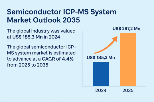
The semiconductor industry is entering a new era of complexity with shrinking device nodes, multilayered architectures, and growing sensitivity to material purity. In this evolving environment, Inductively Coupled Plasma Mass Spectrometry (ICP-MS) systems have become essential for semiconductor manufacturers. These systems provide high-resolution, multi-element analysis at ultra-trace levels, enabling manufacturers to detect and eliminate even minute contaminants during production.
Valued at US$ 185.3 Mn in 2024, the global semiconductor ICP-MS system market is projected to reach US$ 297.2 Mn by 2035, showcasing a robust CAGR of 4.4%. This growth is largely attributed to rising demand for advanced semiconductor manufacturing technologies, yield improvement measures, and regional investments in R&D.
Market Drivers & Trends
Increasing Focus on Yield Improvement and Defect Reduction As semiconductor devices become more complex and miniaturized, even the slightest impurity can result in performance degradation or device failure. ICP-MS systems enable trace-level detection of contaminants in raw materials, wafers, and finished chips. This precise analysis helps in reducing defects and improving overall production yields, which is crucial for applications in sectors such as automotive electronics, aerospace, and medical devices.
Rising Demand for Advanced Manufacturing Processes The global surge in 5G deployment, AI integration, electric vehicles, and consumer electronics demands highly efficient and pure semiconductor components. As a result, semiconductor fabs are investing in advanced analytical instrumentation like ICP-MS to support next-generation chip fabrication.
Regulatory Pressure & Environmental Monitoring With increasing global focus on environmental protection, the semiconductor industry is required to comply with stringent material safety and emission standards. ICP-MS systems are pivotal in this context, offering compliance assurance through accurate trace element detection.
Latest Market Trends
Shift Toward High-Resolution Systems: In 2024, High Resolution ICP-MS accounted for 54.1% of the market share and is expected to grow at a CAGR of 4.8%. These systems are highly valued for their enhanced sensitivity and ability to detect ultratrace elements critical to semiconductor reliability.
Process Automation and Smart Integration: Recent systems are being designed with enhanced software, automation, and remote monitoring features. This aligns with the semiconductor industry's push toward Industry 4.0 adoption and process optimization.
Triple Quadrupole ICP-MS Gaining Momentum: For applications involving complex matrices, Triple Quadrupole ICP-MS is emerging as a preferred solution due to its accuracy, lower detection limits, and interference removal capabilities.
Key Players and Industry Leaders
Key companies shaping the semiconductor ICP-MS system landscape include:
Agilent Technologies Inc.
Thermo Fisher Scientific Inc.
PerkinElmer Inc.
Shimadzu Corporation
Analytik Jena GmbH
Applied Spectra
Teledyne CETAC Technologies
Eurofins Scientific
Intertek Group, Inc.
Nu Instruments
Skyray Instruments USA, Inc.
These players are actively investing in product innovation, strategic collaborations, and R&D initiatives to strengthen their market presence.
Recent Developments
In October 2024, Thermo Fisher Scientific launched the iCAP MX Series ICP-MS, which includes single and triple quadrupole systems. Designed for environmental and industrial laboratories, these instruments improve trace element detection capabilities across various materials, supporting high-stakes applications including semiconductor fabrication.
Agilent Technologies continues to expand its modular platforms with enhanced software and data analytics tools to aid real-time quality monitoring in semiconductor manufacturing lines.
Gain a preview of important insights from our Report in this sample –
Market Opportunities
Emerging Applications in AI and EVs: As AI chips and EV power modules become mainstream, the need for ultra-clean, high-performance semiconductors will increase. ICP-MS systems are vital in ensuring the required material standards.
Integration with Smart Fab Technology: Growing interest in automated, sensor-driven semiconductor fabs presents opportunities for integrating ICP-MS systems into digital twins and predictive maintenance platforms.
Growth in Outsourced Semiconductor Manufacturing: The rise of fabless companies and semiconductor foundries is creating new demand for analytical instrumentation that supports cross-vendor process validation.
Future Outlook
Looking ahead, the semiconductor ICP-MS system market is expected to evolve in tandem with semiconductor technology advancements. Miniaturization trends, increasing need for zero-defect manufacturing, and regulatory compliance will drive long-term growth. Additionally, increased R&D activity in material science and nanotechnology will fuel innovation in ICP-MS instrumentation and applications.
Market Segmentation
The global market is segmented by:
Offering: Hardware (detector, pump, torch, cones), Software, and Services
Technology: Quadrupole Based ICP-MS, Multicollector ICP-MS, High Resolution ICP-MS, Single/Triple Quadrupole ICP-MS
Deployment: Benchtop, Floor-standing
Installation: Laboratory, Process
Application: Wafer, Slurry, Process Chemicals, Organic & Metal Analysis
End-use: Integrated Device Manufacturers (IDM), Foundries
Regional Insights
Asia Pacific leads the global market, accounting for 52.4% share in 2024, and is expected to maintain its dominance with a CAGR of 4.8%. Major semiconductor powerhouses such as Taiwan, South Korea, China, and Japan are driving this leadership through extensive production infrastructure and R&D investments.
North America: The presence of key industry players and innovation hubs makes it a significant contributor.
Europe: Countries like Germany and France are investing in local semiconductor production and analytical instrumentation.
Rest of World: Markets in ASEAN and India are emerging, driven by electronics demand and investment-friendly policies.
Why Buy This Report?
In-depth analysis of the global semiconductor ICP-MS system market dynamics, trends, and forecasts through 2035
Comprehensive company profiles and recent strategic developments
Regional and country-level market breakdowns
Technological segmentation and future outlook by deployment, application, and end-use
Insights into competitive landscape and market share by key players
Cross-segment and value chain analysis for informed decision-making
Frequently Asked Questions (FAQs)
Q1. What is the market size of the semiconductor ICP-MS system market in 2024? A1. The market was valued at US$ 185.3 Mn in 2024.
Q2. What is the projected market value by 2035? A2. It is expected to reach US$ 297.2 Mn by 2035.
Q3. What is the CAGR for the forecast period 2025–2035? A3. The market is projected to grow at a CAGR of 4.4%.
Q4. Who are the leading players in this market? A4. Major companies include Agilent Technologies, Thermo Fisher Scientific, PerkinElmer, and Shimadzu Corporation, among others.
Q5. Which region dominates the market? A5. Asia Pacific is the leading region, driven by strong semiconductor manufacturing activity.
Q6. What trends are shaping the market? A6. Trends include rising demand for high-resolution systems, smart fab integration, and increasing regulatory compliance needs.
About Transparency Market Research Transparency Market Research, a global market research company registered at Wilmington, Delaware, United States, provides custom research and consulting services. Our exclusive blend of quantitative forecasting and trends analysis provides forward-looking insights for thousands of decision makers. Our experienced team of Analysts, Researchers, and Consultants use proprietary data sources and various tools & techniques to gather and analyses information. Our data repository is continuously updated and revised by a team of research experts, so that it always reflects the latest trends and information. With a broad research and analysis capability, Transparency Market Research employs rigorous primary and secondary research techniques in developing distinctive data sets and research material for business reports. Contact: Transparency Market Research Inc. CORPORATE HEADQUARTER DOWNTOWN, 1000 N. West Street, Suite 1200, Wilmington, Delaware 19801 USA Tel: +1-518-618-1030 USA - Canada Toll Free: 866-552-3453 Website: https://www.transparencymarketresearch.com Email: [email protected]
0 notes
Photo

TSMC is set to open its first chip design center in Munich, Germany, marking a major step in expanding European semiconductor industry. This facility will help local and European chip developers optimize their designs for TSMC’s advanced process technology, bridging the gap between product design and manufacturing. The Munich center, the company's tenth, will support everything from automotive microcontrollers to AI and HPC processors. By establishing this hub, TSMC aims to strengthen partnerships and accelerate chip innovation across Europe. This move highlights the revival of European chip development and emphasizes TSMC’s commitment to global semiconductor leadership. With Europe’s growing focus on chip independence, such initiatives foster local talent and innovation. Are you excited to see more European advancements in chip technology? Would you like to learn how this impacts the global electronics supply chain? Let us know your thoughts! Follow us for more updates on semiconductor industry breakthroughs and tech innovations. #TSMC #Semiconductors #ChipDesign #EuropeTech #TechInnovation #Automation #AI #HPC #NanoTech #GlobalTech #Manufacturing #Fabs #EuropeanIndustry
0 notes
Text
Custom Cotton T-Shirts: How Manufacturers Help Bring Your Creative Vision to Life

In the age of personalized branding and fast fashion, custom cotton T-shirts have emerged as a favorite canvas for creativity. Whether you're launching a new clothing line, creating event merchandise, or promoting your business, custom T-shirts offer an affordable, versatile, and stylish way to communicate your message. But turning a design idea into a high-quality wearable product doesn’t happen on its own—that’s where professional cotton T-shirt manufacturers play a pivotal role.
From fabric selection to design execution and packaging, these manufacturers bring expertise, technology, and craftsmanship together to help you transform your ideas into wearable art. Here's how they do it.
1. Helping You Choose the Right Fabric
Every successful custom T-shirt begins with the right fabric. Cotton is a preferred material due to its breathability, softness, durability, and skin-friendly nature. However, there are various cotton options to choose from—combed cotton, organic cotton, ring-spun cotton, and cotton blends with polyester or spandex.
Manufacturers guide you through these options based on your design needs, price point, and target audience. For example, organic cotton is ideal for eco-conscious brands, while ring-spun cotton offers a smoother finish for high-resolution prints.
2. Offering Flexible Customization Options
Modern T-shirt manufacturers provide a wide range of customization capabilities to bring your ideas to life. Some of the most common include:
Screen Printing – Ideal for bold, vibrant graphics and larger orders
Direct-to-Garment (DTG) Printing – Perfect for small batches and photo-quality designs
Embroidery – Adds a high-end, textured look for logos and monograms
Sublimation and Heat Transfer – Suitable for full-color or edge-to-edge prints
Manufacturers can recommend the most suitable method based on your artwork, color complexity, order volume, and garment type.
3. Design Support and Sampling
If you're not a design expert, most manufacturers offer in-house design teams or digital mockup tools to help refine your artwork. They ensure proper alignment, color accuracy, and size scaling, so your vision is translated perfectly onto the fabric.
Reputable manufacturers also provide sample production, allowing you to review and approve the final look and feel before moving into full-scale manufacturing. This ensures consistency and minimizes costly errors.
4. Scaling for Bulk Production Without Losing Quality
A major advantage of working with established cotton T-shirt manufacturers is their ability to scale production efficiently while maintaining consistent quality. Whether you need 50 pieces or 50,000, they implement quality control protocols at each step—cutting, stitching, printing, and packaging—to ensure that every T-shirt meets your specifications.
Advanced machinery and automation allow for faster turnaround times, while human oversight ensures the artisanal touches remain intact.
5. Private Labeling and Brand Packaging
To help your custom T-shirt line stand out, many manufacturers offer private labeling services—including branded neck tags, hang tags, woven labels, and custom packaging. These finishing touches add professionalism and brand identity to your product.
This is especially valuable for fashion startups and e-commerce brands looking to create a cohesive and memorable unboxing experience.
6. Eco-Friendly Manufacturing Options
If sustainability is part of your brand's DNA, many manufacturers now offer eco-conscious production methods. This includes using organic or recycled cotton, water-based inks, and ethical labor practices.
By partnering with a responsible manufacturer, you not only bring your creative vision to life—you do it in a way that aligns with modern consumer values.
Conclusion
Creating custom cotton T-shirts is more than just printing a design—it’s about collaborating with professionals who understand fabric, design, technology, and branding. From choosing the right cotton blend to perfecting the print and ensuring scalable production, cotton T-shirt manufacturers are the creative and logistical bridge between your vision and your final product.
Whether you’re a fashion entrepreneur, event planner, or brand builder, partnering with the right manufacturer ensures your ideas are brought to life with quality, consistency, and impact.
0 notes
Text
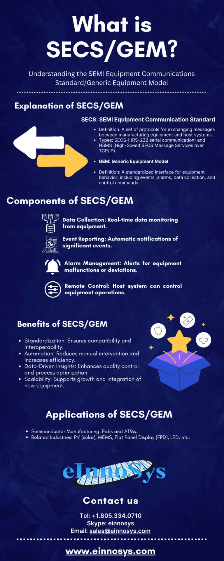
What is SECS/GEM? Understanding the SEMI Equipment Communications Standard/Generic Equipment Model
#secs/gem#secs/gem software#semiconductor#equipment software#secs gem software#secs/gem protocol#fab automation
0 notes
Text
Semiconductor Manufacturing Equipment Market Drivers Shaping Global Industry Growth and Technological Innovation Trends
The semiconductor manufacturing equipment market plays a crucial role in the broader semiconductor industry by providing the essential machinery and tools used to produce integrated circuits and microchips. These chips power everything from smartphones and computers to automobiles and medical devices. Understanding the primary market drivers behind this sector reveals why it continues to experience rapid growth and why manufacturers, suppliers, and investors are keenly focused on its development.

Growing Demand for Advanced Semiconductor Devices
One of the most significant drivers of the semiconductor manufacturing equipment market is the soaring demand for advanced semiconductor devices. The rapid adoption of technologies such as 5G, artificial intelligence (AI), cloud computing, and the Internet of Things (IoT) has drastically increased the need for high-performance chips. These technologies require smaller, faster, and more energy-efficient chips, prompting semiconductor manufacturers to upgrade their equipment and processes continuously.
Advanced semiconductor nodes, such as 7nm and below, require highly sophisticated equipment to maintain precision and yield. As chipmakers push the boundaries of Moore’s Law, the complexity of wafer fabrication grows, necessitating cutting-edge lithography machines, etching tools, and deposition systems. The growing demand for these next-generation chips directly fuels the semiconductor manufacturing equipment market.
Technological Innovations and Industry Trends
The semiconductor equipment market is heavily influenced by continuous technological innovation. Equipment manufacturers are investing substantially in research and development to create tools that can handle the increasing complexity of chip fabrication. Innovations such as extreme ultraviolet (EUV) lithography have revolutionized the ability to produce smaller nodes, which are essential for advanced semiconductor devices.
Additionally, there is a strong emphasis on automation and smart manufacturing within semiconductor fabs. The integration of AI and machine learning technologies into manufacturing equipment helps improve process control, enhance yield rates, and reduce production costs. These trends drive equipment upgrades and new installations, positively impacting the market.
Rising Investments in Semiconductor Fabrication Facilities
Governments and private enterprises worldwide are increasing investments in semiconductor fabrication plants, often called fabs. These capital-intensive facilities require state-of-the-art manufacturing equipment to produce chips at scale. Recent geopolitical shifts and supply chain concerns have prompted countries to promote domestic semiconductor production, leading to a surge in fab construction projects.
Substantial financial commitments by countries such as the United States, China, South Korea, and the European Union aim to secure supply chains and foster technological self-reliance. The establishment of new fabs and expansion of existing ones directly boosts demand for semiconductor manufacturing equipment, as manufacturers must procure the latest tools to build competitive production lines.
Growing Use of Semiconductors Across Diverse Industries
The expanding application of semiconductor devices across various industries also propels the demand for semiconductor manufacturing equipment. Beyond traditional consumer electronics, sectors such as automotive, healthcare, aerospace, and industrial automation increasingly rely on advanced chips.
The automotive industry's transition toward electric vehicles (EVs) and autonomous driving technologies requires complex semiconductor solutions. These demand significant fabrication capabilities, encouraging chipmakers to invest in sophisticated equipment. Similarly, healthcare innovations, including wearable devices and diagnostic tools, further expand the market scope for semiconductor manufacturing machinery.
Demand for Miniaturization and Enhanced Performance
Consumer expectations for smaller, lighter, and more powerful electronic devices compel semiconductor manufacturers to develop chips with greater functionality in smaller form factors. Achieving this miniaturization involves advanced equipment capable of handling nanoscale fabrication.
The performance requirements of modern applications, such as augmented reality (AR), virtual reality (VR), and high-speed data processing, intensify the need for innovative manufacturing tools. The drive for enhanced chip performance encourages equipment manufacturers to innovate and supply tools that enable high precision, reduced defects, and improved throughput.
Environmental and Energy Efficiency Regulations
Stringent environmental regulations and growing emphasis on sustainability have a considerable impact on the semiconductor manufacturing equipment market. Semiconductor fabs consume significant amounts of energy and water and generate waste during production.
To comply with environmental standards and reduce operating costs, fabs seek advanced equipment that supports cleaner and more energy-efficient manufacturing processes. Equipment providers respond by designing systems that minimize chemical usage, optimize power consumption, and facilitate waste reduction, further fueling market growth.
Supply Chain Challenges and Strategic Equipment Sourcing
Recent supply chain disruptions have highlighted the importance of robust semiconductor manufacturing capabilities. Companies are investing in advanced equipment to localize and secure chip production, mitigating risks associated with global dependencies.
This strategic shift supports the demand for semiconductor manufacturing tools domestically and regionally. Equipment manufacturers benefit from increased orders as semiconductor producers diversify their manufacturing bases, aiming for supply chain resilience.
Rising Demand for Specialty Chips and Customization
The growing requirement for specialty and custom-designed chips for specific applications also drives the semiconductor manufacturing equipment market. Chips tailored for AI acceleration, graphics processing, and cybersecurity necessitate distinct fabrication processes.
To accommodate these demands, fabs require flexible and specialized equipment capable of producing diverse chip types. This diversification pushes equipment manufacturers to innovate and expand their product portfolios, stimulating market expansion.
In summary, the semiconductor manufacturing equipment market is propelled by a combination of rising demand for advanced semiconductor devices, technological innovation, increased fab investments, expanding industry applications, and regulatory factors. The market’s growth trajectory is supported by the relentless push toward miniaturization, improved performance, and sustainability. As global demand for semiconductors continues to rise, driven by evolving technologies and industries, the semiconductor manufacturing equipment market is poised for sustained expansion and dynamic transformation.
#SemiconductorManufacturingMarket#ChipTechnology#SemiconductorEquipment#TechInnovation#AdvancedSemiconductors
0 notes
Text
Wafer Sorters Market to Reach $582.9 Million by 2035
According to the latest research by DataString Consulting, the global Wafer Sorters market is projected to grow from $320.1 million in 2024 to $582.9 million by 2035, registering a compound annual growth rate (CAGR) of 5.6% over the forecast period.
Detailed Analysis - https://datastringconsulting.com/industry-analysis/wafer-sorters-market-research-report
The increasing adoption of semiconductor testing, photovoltaic manufacturing, MEMS production, and integrated circuit (IC) fabrication is driving this robust market expansion.
Key Applications and Demand Drivers
Wafer Sorters play an essential role in the semiconductor manufacturing process by automating wafer handling and improving process throughput, accuracy, and contamination control. Primary areas of use include:
Semiconductor Testing: Enables high-speed, high-precision wafer identification and placement.
Photovoltaic Cell Production: Supports consistent wafer sorting to meet high-efficiency standards.
MEMS and IC Manufacturing: Ensures clean handling in highly sensitive production environments.
The demand surge is further amplified by the global shift toward miniaturized electronics, 5G infrastructure, and advanced driver-assistance systems (ADAS), all of which depend on streamlined wafer processing workflows.
Industry Trends Fueling Growth
The market is witnessing technological advancements in wafer sorter designs, including:
AI-driven sorting systems for predictive maintenance and reduced downtime
IoT-enabled devices for real-time data acquisition and monitoring
Integration with Industry 4.0 frameworks for enhanced automation and process transparency
These innovations are enabling manufacturers to handle increasing wafer sizes, higher throughput requirements, and stringent yield expectations in modern fabs.
Competitive Landscape
The Wafer Sorters market is highly competitive and features a range of global leaders who are continuously innovating and forming strategic partnerships to maintain a technological edge. Prominent companies include:
Applied Materials Inc.
Brooks Automation Inc.
Disco Corporation
EV Group
Hitachi High-Technologies Corporation
Kulicke and Soffa Industries Inc.
Lam Research Corporation
Nikon Corporation
Rudolph Technologies Inc.
SCREEN Semiconductor Solutions Co. Ltd.
Tokyo Electron Limited
Ulvac Inc.
These companies are investing in R&D to deliver next-generation wafer sorters with greater modularity, energy efficiency, and compatibility across fab ecosystems.
Regional Growth Outlook
North America and Asia-Pacific remain the two most dynamic regions for the Wafer Sorters market, driven by:
Strong presence of semiconductor fabrication plants
Government support for chip self-sufficiency
Increased consumer demand for electronic devices and automotive innovations
Key markets such as the U.S., China, Japan, Taiwan, and South Korea lead in both technology adoption and production volume. Meanwhile, India, Brazil, and South Africa are emerging as attractive destinations for market expansion due to evolving local semiconductor ecosystems and favorable government policies.
Supply Chain Evolution
As demand intensifies, the Wafer Sorters supply chain—from raw materials and component manufacturing to machine assembly and end-use deployment—is expected to undergo significant transformation. Companies are likely to:
Invest in local sourcing and nearshoring
Strengthen partnerships with OEMs and system integrators
Adopt flexible manufacturing models to respond faster to custom demands
These adaptations will help players stay competitive and ensure uninterrupted delivery in an increasingly complex and globalized supply environment.
Market Segmentation Highlights
The market study by DataString Consulting offers detailed insights across key segments, including:
Product Type: Fully-Automated, Semi-Automated, Manual
End-Users: Foundries, IDM Manufacturers, R&D Labs
Usage Frequency: High-Throughput, Low-Volume/Prototype
Technology Integrated: Optical Sensors, RFID, AI/ML-Enhanced
Pricing Models: Entry-Level, Mid-Range, Premium
These segmentations allow stakeholders to pinpoint high-growth opportunities and align investments accordingly.
About DataString Consulting
DataString Consulting is a trusted name in strategic market research, offering tailored insights for both B2B and B2C enterprises. We support our clients in TAM expansion, go-to-market strategy, and competitive intelligence by analyzing trends, customer behavior, and market dynamics across more than 15 industries and 60 sub-industries.
With over 30 years of combined leadership experience, our team delivers precise, data-backed strategies that filter out noise and help clients capitalize on actionable opportunities.
We deliver industry-specific market research solutions designed to reduce the time between product development and market fit—ensuring our clients stay ahead in rapidly evolving sectors.
0 notes
Text
Industry 4.0 on the Rise: Smart Factory Market to Surpass $220B by 2034 🏭📈

Smart Factory Market is on a strong upward trajectory, projected to grow from $86.2 billion in 2024 to an impressive $221.7 billion by 2034, at a compound annual growth rate (CAGR) of 9.9%. This growth reflects the global push towards digital transformation, with manufacturers adopting advanced technologies such as IoT (Internet of Things), AI (Artificial Intelligence), robotics, and machine learning to automate operations, reduce downtime, and boost productivity. Smart factories represent the evolution of traditional manufacturing into intelligent, self-optimizing environments that enhance decision-making through real-time data and analytics.
Market Dynamics
Smart factory solutions are revolutionizing industries by improving operational efficiency, ensuring product quality, and supporting sustainability goals. The market’s backbone lies in manufacturing execution systems (MES), predictive maintenance tools, and automated quality control. Factors fueling growth include the increasing demand for industrial automation, advancements in connectivity (5G and edge computing), and the need for energy-efficient production systems.
Click to Request a Sample of this Report for Additional Market Insights: https://www.globalinsightservices.com/request-sample/?id=GIS20453
However, challenges such as high initial setup costs, cybersecurity risks, and integration of legacy infrastructure can slow adoption, especially among small and medium-sized enterprises. Despite these hurdles, the potential return on investment through long-term cost savings and improved throughput continues to drive implementation across sectors like automotive, aerospace, healthcare, and electronics.
Key Players Analysis
The market landscape is shaped by industry giants including Siemens AG, Schneider Electric, Honeywell International Inc., ABB, Rockwell Automation, Emerson Electric, and Mitsubishi Electric. These companies are investing heavily in R&D to stay ahead in a rapidly evolving field. Their solutions span from control devices and sensors to AI-enabled software platforms that enhance factory agility.
Meanwhile, emerging innovators like Factory Sense, Smart Fab Solutions, and Digitize Manufacture are introducing niche products that cater to customizable and flexible production environments. These players are leveraging smart data, modular architecture, and collaborative robotics to appeal to a growing customer base that values adaptability and innovation.
Regional Analysis
North America leads in smart factory adoption, particularly the United States, which boasts robust industrial infrastructure and a strong focus on digital transformation. The region’s automotive and aerospace industries are significant adopters of smart technologies, driven by stringent quality requirements and performance optimization.
Europe closely follows, with countries like Germany and the UK driving growth through Industry 4.0 initiatives and regulations aimed at sustainable manufacturing. The region’s emphasis on carbon reduction, energy efficiency, and green technologies supports the expansion of smart factory solutions.
The Asia-Pacific region is emerging as the fastest-growing market. China, Japan, and South Korea are at the forefront, supported by rapid industrialization, government incentives, and a massive electronics manufacturing base. With strong demand for consumer goods and rising labor costs, the adoption of smart technologies in these economies is accelerating significantly.
Recent News & Developments
The market has recently seen a surge in strategic collaborations and partnerships aimed at enhancing technological capabilities. Leading firms are integrating AI and IoT into core operations, improving factory uptime and production flexibility. The shift toward cloud-based deployment models and hybrid systems has gained momentum, offering scalability and real-time remote access to critical operations.
Additionally, there’s growing interest in cybersecurity frameworks to safeguard sensitive industrial data. New solutions emphasize resilience, with embedded machine learning models that detect anomalies and prevent potential disruptions. Furthermore, global regulatory focus on environmental sustainability is driving innovation in low-emission and energy-efficient smart manufacturing systems.
Browse Full Report : https://www.globalinsightservices.com/reports/smart-factory-market/
Scope of the Report
This report offers a comprehensive look into the Smart Factory Market, covering historical trends (2018–2023) and future forecasts (2025–2034). It provides qualitative and quantitative insights across segments such as technology (AI, IIoT, Big Data), deployment models (on-premise, cloud, hybrid), and end users (automotive, food & beverages, electronics, etc.).
Beyond market size and growth projections, the report delves into regional performance, competitive landscape, emerging players, and regulatory dynamics. Key development strategies like mergers, acquisitions, new product launches, and cross-industry collaborations are also evaluated. With its rich data analysis, the report equips stakeholders with strategic insights to navigate the evolving smart manufacturing landscape.
Discover Additional Market Insights from Global Insight Services:
High Speed Cable Market : https://www.globalinsightservices.com/reports/high-speed-cable-market/
Advanced Semiconductor Packaging Market ; https://www.globalinsightservices.com/reports/advanced-semiconductor-packaging-market/
Agricultural Lighting Market : https://www.globalinsightservices.com/reports/agricultural-lighting-market/
Air Quality Monitoring System Market ; https://www.globalinsightservices.com/reports/air-quality-monitoring-system-market/
Industrial Robotics Market : https://www.globalinsightservices.com/reports/industrial-robotics-market/
#smartfactory #industry40 #automation #manufacturingtechnology #iotinmanufacturing #artificialintelligence #predictivemaintenance #robotics #digitaltransformation #industrialautomation #iiot #mes #cloudmanufacturing #cybersecurity #smartmanufacturing #bigdata #machinelearning #edgecomputing #plc #erp #smartfactories #automotiveindustry #electronicsmanufacturing #aerospaceinnovation #supplychainoptimization #realtimemonitoring #energyoptimization #sustainablemanufacturing #processautomation #futureofmanufacturing #connectedfactory #intelligentautomation #smartfactorysolutions #manufacturinginnovation #cobots #cloudintegration #datadrivenmanufacturing #remotemonitoring #digitalsupplychain #greentechnology #manufacturingefficiency
About Us:
Global Insight Services (GIS) is a leading multi-industry market research firm headquartered in Delaware, US. We are committed to providing our clients with highest quality data, analysis, and tools to meet all their market research needs. With GIS, you can be assured of the quality of the deliverables, robust & transparent research methodology, and superior service.
Contact Us:
Global Insight Services LLC 16192, Coastal Highway, Lewes DE 19958 E-mail: [email protected] Phone: +1–833–761–1700 Website: https://www.globalinsightservices.com/
0 notes
Text
Faridabad’s Leading Belt Conveyor Companies You Should Know
In today’s fast-paced industrial environment, efficient material handling is not just an operational requirement but a competitive advantage. Belt conveyors—a staple in manufacturing, logistics, and warehousing—are critical to ensuring smooth product flow and reducing manual handling time. When it comes to sourcing these essential systems in India, Faridabad stands out as a leading manufacturing hub.
This blog explores the top belt conveyor companies in Faridabad, highlighting their strengths, innovations, and what sets them apart. If you’re looking to invest in a high-performance conveyor solution, this guide will help you make an informed decision.
Why Faridabad Is a Belt Conveyor Manufacturing Hub
Part of the Delhi-NCR industrial belt and situated in Haryana, Faridabad has made a name for itself as a manufacturing hub for machinery and equipment. Its prominence in the belt conveyor manufacturing industry is a result of several factors:
Well-developed industrial infrastructure
Proximity to Delhi, Gurgaon, and major logistics corridors
Access to skilled labor and engineering talent
Presence of diverse industries driving demand
Supportive government policies for MSMEs and exporters
Thanks to this ecosystem, many belt conveyor manufacturers in Faridabad are now serving both domestic and global markets with world-class products.
What Makes a Good Belt Conveyor Manufacturer?
Before we delve into the top companies, here are the criteria that make a conveyor manufacturer stand out:
Engineering expertise and customization capability
High-quality raw materials and precision fabrication
Advanced automation integration (motors, PLCs, sensors)
Customer-centric approach with timely delivery
Strong after-sales support and spare parts availability
Compliance with safety and quality standards (ISO, CE)
Now, let’s look at the companies in Faridabad that embody these traits.
Top Belt Conveyor Companies in Faridabad
1. Neo Conveyors
Neo Conveyors is one of the most recognized names in the conveyor system manufacturing sector in Faridabad. Known for their custom-engineered belt conveyors, they cater to industries like cement, food processing, mining, packaging, and more.
Key Strengths:
Custom designs for bulk material handling
High-performance conveyors with minimal maintenance
Export-ready systems with CE certifications
2. Conveline Systems Pvt. Ltd.
Conveline Systems specializes in modular conveyor solutions, including belt conveyors, roller conveyors, and inclined systems. Their systems are widely used in e-commerce, warehousing, and packaging industries.
Key Features:
Modular, plug-and-play designs
Quick lead times and scalable systems
High-quality belts and automation-ready features
3. Jay Engineering
Established for over 20 years, Jay Engineering is known for its heavy-duty and precision conveyors. They manufacture industrial-grade belt conveyors for tough environments like foundries and assembly lines.
USP:
Rugged construction with high load capacities
Turnkey project execution with layout planning
Long-life motors and accessories
4. Saifi Con-Fab System Pvt. Ltd.
A pioneer in conveyor technology, Saifi Con-Fab offers advanced belt conveyor solutions for industries ranging from food to electronics. Their R&D-focused approach ensures innovative designs and automation integration.
Highlights:
In-house design and engineering team
Belt conveyors with integrated sensors and safety systems
Strong service support across India
5. Essar Engineers
Essar Engineers delivers a range of material handling equipment, with belt conveyors as one of their core offerings. Their strength lies in delivering high-quality products with fast turnaround times.
Specialties:
Standard and custom belt conveyors
Powder-coated and stainless steel options
Cost-effective and durable solutions
Key Features of Belt Conveyors from Faridabad
Belt conveyors manufactured in Faridabad offer a blend of quality, reliability, and cost-efficiency. Here are some common features:
✅ Sturdy Frame Construction
Made from mild steel, aluminum, or stainless steel for durability and resistance to corrosion.
✅ Custom Belt Materials
Options include PVC, rubber, modular plastic, and food-grade belts depending on the application.
✅ Adjustable Speeds and Height
Motorized speed control with VFDs and adjustable-height frames for operational flexibility.
✅ Portability and Compact Design
Many companies offer portable or foldable conveyors for smaller facilities.
✅ Automation-Ready
For smooth automation, sensors, smart controllers, and PLC systems are integrated.
Applications of Belt Conveyors
Many different businesses use belt conveyors manufactured in Faridabad:
Automotive: Assembly line movement and component transfer
FMCG: Carton and pouch transport in packaging lines
E-commerce & Warehousing: Sorting and order fulfillment
Pharmaceuticals: Clean, contamination-free product handling
Mining & Cement: Heavy-duty material transfer
Food Processing: Hygienic conveyors with wash-down features
Their adaptability and versatility make them essential across sectors.
Why Choose Faridabad Manufacturers?
Here’s why companies across India and abroad trust Faridabad belt conveyor manufacturers:
📈 Proven Experience
Many companies have decades of experience and serve top national brands.
💡 Engineering Expertise
Access to modern tools like AutoCAD, SolidWorks, and simulation testing ensures quality.
🌍 Export Capability
Several firms export to Middle East, Africa, and Southeast Asia, indicating trust and scalability.
💸 Competitive Pricing
Compared to imported systems, Faridabad manufacturers offer high performance at a lower cost.
🔧 Reliable After-Sales Support
Prompt service and availability of parts ensure minimal downtime.
Things to Consider Before Buying
The following should be taken into account while selecting a belt conveyor system:
The kind and volume of information that needs to be conveyed
The type and amount of information that must be communicated
Required speed and length of the conveyor
Inclination or level transfer
Environmental factors (temperature, moisture, hygiene)
Power source and space availability
Most manufacturers in Faridabad offer free consultations and site visits to recommend the right solution.
Final Thoughts
If you’re looking to optimize your material handling operations, belt conveyors are a smart investment—and there’s no better place to source them than Faridabad. With a blend of innovation, affordability, and manufacturing excellence, Faridabad’s conveyor companies are meeting the evolving needs of industries across India and beyond.
Whether you're a small business or a large enterprise, the right conveyor partner from Faridabad can help boost your productivity and operational efficiency.
📞 Ready to Upgrade?
Get in touch with Faridabad’s leading belt conveyor manufacturers today for customized solutions and expert guidance.
Address: Plot No. 7, Gali no 2 Sahupura Industrial Area, Near Bypass, Faridabd-121004 Haryana (India)
Phone No. : 9958352003
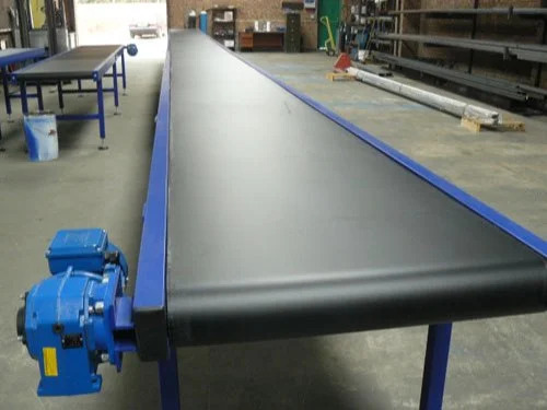
#BeltConveyor#BeltConveyorManufacturer#ConveyorManufacturerFaridabad#MaterialHandlingEquipment#IndustrialConveyors#FaridabadIndustry#ConveyorSystemsIndia#ManufacturingSolutions#FactoryAutomation#BeltConveyorIndia#CustomConveyor#IndustrialMachinery#MadeInIndia#EngineeringSolutions#VashnaviConveyor#FaridabadManufacturers#AutomationEquipment#HeavyDutyConveyors#SmartMaterialHandling#ConveyorBeltSystem
0 notes