#Crystal oscillator circuits
Explore tagged Tumblr posts
Visit Tumblr Blog
Explore Tumblr blogs with no restrictions, modern design and the best experience.
Last Seen Tumblr Blogs


Fun Fact
Tumblr’s website traffic is steadily declining.
Text
https://www.futureelectronics.com/p/electromechanical--timing-devices--crystals/ecs-73-20-5px-tr-ecs-inc.-2022144
Electronic timing system, quartz crystal, Crystal oscillator circuits
CSM-7X Series 7.3728 MHz ±30 ppm 20 pF -10 to +70 °C SMT Quartz Crystal
#ECS Inc.#ECS-73-20-5PX-TR#Frequency Control & Timing Devices#Crystals#chip systems#Watch crystal#tuning fork crystals#solutions#quartz crystal#Crystal oscillator circuits#electronic timing systems#wireless#timing ic
1 note
·
View note
Text
https://www.futureelectronics.com/p/electromechanical--timing-devices--crystals/ecs-73-20-5px-tr-ecs-inc.-2022144
Crystal oscillator circuit, Resonator timing device, crystal oscillator circuit
CSM-7X Series 7.3728 MHz ±30 ppm 20 pF -10 to +70 °C SMT Quartz Crystal
#ECS Inc.#ECS-73-20-5PX-TR#Frequency Control & Timing Devices#Crystals#Resonator timing device#crystal oscillator circuit#frequency Timing solution#Surface Mount Tuning Fork#electronic timing system#Quartz crystal circuit
1 note
·
View note
Text
https://www.futureelectronics.com/p/electromechanical--timing-devices--crystals/rsm200s-32-768-12-5-tr-raltron-1457787
Frequency Control & Timing Devices, Crystals, RSM200S-32.768-12.5-TR, Raltron
RSM200S Series 32.768 kHz ±20 ppm 12.5 pF -10 to +60 °C SMT Tuning Fork Crystal
#Frequency Control#Timing Devices#Crystals#RSM200S-32.768-12.5-TR#Raltron#Wireless timing#quartz#hardware#Low Profile Crystal#crystal oscillator circuit#electronic timing device#timing system software#quartz crystal#diode array#Watch crystal
1 note
·
View note
Text
Stepping Backwards a Bit (or 24)
I was looking for a simpler project. My recent 68030 work has been challenging and really pushing the limits of what I can do. I wanted something I could work on, but perhaps where someone else has already worked out the hardest parts.
I find laying out PCBs to be rather relaxing. It's one of those repetitive, almost meditative tasks, like needlepoint or whittling. The kind of hobby where I can turn on some music or a comfortable old TV show, zone out for a few hours, and wake up to this new thing that I created.
Debugging however is very mentally taxing, and the design work required to have a functional schematic to create a PCB for is an active whole-mind prices. So what I really needed was an existing project I could design a board for.
Enter [Grant Searle]. If you're not familiar with [Grant Searle], he has excellent designs for breadboard computers with a very minimal parts count. I studied his minimal Z80 design when I was first starting to build my own computers and learned a lot from it. I highly recommend his work for anyone who is interested in learning how to build their own computer but doesn't know where to start.
I was recently given a Rockwell 6502 CPU pulled from a dead LED marquee. I've never actually worked with 6502, so this seemed like a good time to try building Grant's 8-chip (or 7-chip) 6502 computer.
A few hours later, I had a PCB design completed, gerbers generated, and an order placed. Less than $5 for 5 boards, including shipping. A couple weeks later they arrived in the mail.


I did end up making a few modifications to [Grant]'s design. Instead of a clock circuit made from a discrete crystal and a couple inverter gates, I used a TTL oscillator because I've always found them to be more reliable. I also added support for an FTDI USB Serial adapter chip so that the board can be used with a modern computer as a terminal. And finally, since a PCB is much harder to add new components to relative to a solderless breadboard, I added an expansion header. All of it wrapped up in a compact PCB with lots of helpful silkscreen marking.

I realized after I had ordered the PCBs that the 16kB ROM chips [Grant] used are no longer manufactured or readily available. I have plenty of 8kB EEPROM chips on hand however. Thankfully the OSI BASIC interpreter [Grant] ported to this design fits within 8kB, so I was able to make a few adjustments and re-assemble it to work with the ROM chips I have on hand.
After a small glitch with my EEPROM programmer, it works!

It's quite a change going from my 33MHz+ 68030 to this tiny 6502 running at just under 2MHz. The BASIC text-based Mandelbrot renderer that completes in seconds on my 68030 takes four and a half minutes on the 6502. Not bad at all, considering my bus-impaired 68000 build takes 9 minutes to do the same.
This was a fun little project. It was a nice little break from some of the more difficult projects I've been working on. I have shared the project on GitHub for anyone who might want to take a look.
I hope to have this project with me this weekend, June 14-16, 2024 at Vintage Computer Festival Southwest. I'll be at table 207 in the Tandy Assemble hall, just across the street from the main exhibit hall.
30 notes
·
View notes
Text

Where physics and engineer meet art and neuroscience
Collector:hippocampus
Where memories are collected
A point, one-dimensional, existing in a sphere, becoming 3-dimensional, emitter, the signal from infra colliculi
A line, the base, a plane that exists, at the basilar artery
V for volume is the equivalent to the sentence that made the point, what exists in the sphere is an angle, the mention of becoming is an aspect, in this trifecta of subject matter exists an energy, frequency, and vibration
The 2nd dimension is the line, what extends outwardly, where that extent reaches is b
B with an arrow pointing back is the remembering of 2D, I being induction, the quantum mechanics*** of that act on the parahippocampal gyrus**, recalling*
Induction to C is angular momentum with parietal lobe of recollecting I with the arrow under b, the magnetic field density, Volume to C is the current to the circuit within
The last 3 sentences are a trisynaptic circuit from a current, from Ic, Ie being the trisynaptic loop and Ve being episodic memory
(C) tuned into a frequency
(E) tapped into a vibration
(B) put out a particular energy
Collector at p is the higher plane of what gathered angular momentum
Base at n is where is the emission was neutralized at length to distribute a wave form
Emitter at p is the lower plane of radiating what made active a line, the comingling of what emitted in time for linear expansion to a frequency modification and amplitude modulation
Vb, the base for the basal ganglia to behave in a manner that corresponds with angular gyrus****(angular acceleration amplifying a brain wave), as the angles that met amplitude were particles to the amplified modulus, the voluminous flux from descriptions that modified within the frequencies of the axes that orbitted as potential for 3d to be the proportion what became a shape, thus, thought form inducing a state to describe what signaled a blood circuit to crystallize a circulation where Ve is the volume of the energy to encapsulate linearity of encoded information to dispere across channels, the ion to what came to be ionic Vc, the vacuum that coordinated to aspecting the collapse of the wave function, therein, Vce < 0, the entorhinal cortex sensing the postsynaptic axon terminal ending the point, the extending of a nerve to the paraterminal gyrus to begin signaling the beginning*** of Vbe* to a brain function***** what be that as an oscillation amplified is where it is now a wavelength Vbe<0
A neural connection based on a neural current, the vein and insulat cortex from brain stem and emission expressed, from a medium spiky neuron at nucleus accumbens and the pineal gland from astroglial cells
Clearer than before and continually clearing the way
Inner engineering relative to metaphysics, the art of learning and observing
The knot quite possibly tied it all together[indefinitely]
#metaphysics#occult and chill#i can draw this out too#go do your research#i charge for questions#neuroscience#quantum mechanics#reverse engineering#inner engineering#private buddha#black yogi#melanated indigenous folk
3 notes
·
View notes
Text
Electronics Components and Uses:
Here is a list of common electronics components and their uses:
Resistor:
Use: Limits or controls the flow of electric current in a circuit.
Capacitor:
Use: Stores and releases electrical energy; used for filtering, timing, and coupling in circuits.
Inductor:
Use: Stores energy in a magnetic field when current flows through it; used in filters, transformers, and oscillators.
Diode:
Use: Allows current to flow in one direction only; used for rectification, signal demodulation, and protection.
Transistor:
Use: Amplifies and switches electronic signals; fundamental building block of electronic circuits.
Integrated Circuit (IC):
Use: Contains multiple electronic components (transistors, resistors, capacitors) on a single chip; used for various functions like amplification, processing, and control.
Resistor Network:
Use: A combination of resistors in a single package; used in applications where multiple resistors are needed.
Potentiometer:
Use: Variable resistor that can be adjusted to control voltage in a circuit; used for volume controls, dimmer switches, etc.
Varistor:
Use: Protects electronic circuits from excessive voltage by acting as a voltage-dependent resistor.
Light-Emitting Diode (LED):
Use: Emits light when current flows through it; used for indicator lights, displays, and lighting.
Photodiode:
Use: Converts light into an electric current; used in light sensors and communication systems.
Zener Diode:
Use: Acts as a voltage regulator by maintaining a constant voltage across its terminals.
Crystal Oscillator:
Use: Generates a stable and precise frequency; used in clocks, microcontrollers, and communication devices.
Transformer:
Use: Transfers electrical energy between two or more coils through electromagnetic induction; used for voltage regulation and power distribution.
Capacitive Touch Sensor:
Use: Detects touch or proximity by changes in capacitance; used in touchscreens and proximity sensing applications.
Voltage Regulator:
Use: Maintains a constant output voltage regardless of changes in input voltage or load; used for stable power supply.
Relay:
Use: Electromagnetic switch that controls the flow of current in a circuit; used for remote switching and automation.
Fuse:
Use: Protects electronic circuits by breaking the circuit when current exceeds a certain value; prevents damage from overcurrent.
Thermistor:
Use: Resistor whose resistance changes with temperature; used for temperature sensing and compensation.
Microcontroller/Microprocessor:
Use: Processes and controls electronic signals; the brain of many electronic devices and systems.
fig:google-electronics

fig:google-electronics
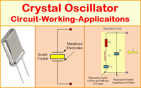
fig:Crystal-Oscillator
This list covers some of the basic electronic components, and there are many more specialized components used for specific applications within the field of electronics.
#electronic#electricity#electric vehicles#electric cars#engineering#semiconductors#wireless#cables#electronics#smartphone#hardware
4 notes
·
View notes
Text
playing satisfactory
i have aluminum shit to do now
still have to get circuit boards, computers, high speed connectors, heavy modular frames, crystal oscillators, smokeless powder, and probably a million other things automated before i can even think about aluminum but i have hazard suits and hover packs now so im happy :3
1 note
·
View note
Text
What Is A TCXO?
A Temperature Compensated Crystal Oscillator (TCXO) is a specially designed oscillator that incorporates a temperature compensation circuit to reduce the impact of temperature fluctuations on the crystal's frequency, ensuring high stability under varying temperature conditions. Compared to traditional crystal oscillators (XO), TCXOs offer greater frequency precision, making them particularly suitable for applications that require strict frequency stability. The typical operating frequency range is from 10 MHz to 52 MHz, with some high-frequency models reaching several hundred MHz.
Get more details: What Is A TCXO?
#electronics#integrated circuits#semiconductor#components#electronic#module#electronic devices#chips#manufacturing#oscillator
0 notes
Text
Global Quartz Crystal Market Outlook: Key Drivers for a 4.3% CAGR by 2034

The Quartz Crystal Market is poised for substantial growth, with its value projected to increase from USD 4.9 billion in 2023 to USD 7.7 billion by 2034, reflecting a CAGR of 4.3% over the forecast period (2024-2034). As industries embrace cutting-edge technologies like 5G networks, IoT devices, and autonomous vehicles, the demand for quartz crystals as essential timing and frequency control components is accelerating across diverse applications.
Quartz crystals play a pivotal role in enabling precise timing and frequency control in a wide range of electronic devices. The market's growth is driven by their indispensable use in automotive electronics, consumer electronics, aerospace and defense, IT and telecommunication, and healthcare industries. The increasing adoption of advanced driver assistance systems (ADAS), connected vehicles, and IoT ecosystems has positioned quartz crystals as critical components in today's rapidly evolving technology landscape.
Access our report for a comprehensive look at key insights - https://www.transparencymarketresearch.com/quartz-crystal-market.html
Key Drivers of Growth
Surging Demand in Consumer Electronics The proliferation of smart devices, including smartphones, wearables, and smart home gadgets, is a significant growth driver. Quartz crystals are vital for ensuring precise timing in oscillators and circuits, which power these devices' seamless operation.
The rise of IoT-enabled devices and connected home solutions further bolsters demand for quartz crystals, as they provide the flawless timing required for data transmission.
Automotive Electronics Boom The automotive industry is experiencing an increased reliance on electronic systems such as infotainment, ADAS, and connectivity modules. These systems demand high-precision timing solutions, which quartz crystals deliver efficiently.
Radar, LiDAR, and camera-based systems for autonomous vehicles are particularly reliant on quartz crystals for synchronization and accuracy.
Advancements in Healthcare and Industrial Automation Quartz crystals are increasingly used in health monitoring devices, precision instruments, and industrial automation systems, contributing to their growing demand in these sectors.
Market Trends
Miniaturization and Power Efficiency Quartz crystal manufacturers are focusing on reducing product size and power consumption, aligning with the demand for portable and energy-efficient devices.
Integration with 5G Networks and IoT The rise of 5G and IoT ecosystems has increased the need for high-frequency, low-latency timing solutions, spurring innovation in quartz crystal technology.
Emergence of Advanced Automotive Systems Autonomous vehicles and ADAS require ultra-reliable timing components, making quartz crystals indispensable in modern automotive electronics.
Key Player Strategies
The market is consolidated, with leading players such as Abracon, ACTE A/S, Diodes Incorporated, ECS Inc. International, FujiCom Co., Ltd, Harmony Electronics Corp, Hefei Jingweite Electronics Co., Ltd, Interquip Electronics (Shenzhen) Co., Ltd, Murata Manufacturing Co., Ltd, Seiko Epson Corp, Shenzhen Jingfeng Crystal Technology Co., Ltd, Siward Crystal Technology Co Ltd, Taitien Electronics Co. Ltd, Yoketan Corporation, Microchip Technology Inc, KYOCERA Corporation, TXC Corporation, Daishinku Corp, NIHON DEMPA KOGYO CO., LTD and others.
Key strategies
Research & Development Investments: Companies are focusing on developing innovative quartz crystal products with improved performance and miniaturized designs.
Strategic Partnerships: Collaborations and acquisitions are being leveraged to expand product portfolios and enter new markets.
Product Launches: For instance, Murata introduced ultra-miniature quartz crystal oscillators tailored for IoT and wearable devices in 2024.
Contact:
Transparency Market Research Inc.
CORPORATE HEADQUARTER DOWNTOWN,
1000 N. West Street,
Suite 1200, Wilmington, Delaware 19801 USA
Tel: +1-518-618-1030
USA - Canada Toll Free: 866-552-3453
Website: https://www.transparencymarketresearch.com
Email: [email protected]
0 notes
Text
USB RTC for Raspberry Pi: The Best Way to Enhance Your Raspberry Pi's Time Accuracy

When it comes to building real-time applications with the Raspberry Pi, one of the most crucial components to ensure is timekeeping. A RTC (Real Time Clock) module provides the Raspberry Pi with a reliable source of time, even when the system is powered off. For those looking to achieve incredibly accurate timekeeping, a USB RTC for Raspberry Pi is a solution that combines the DS3231 RTC chip with a MCP2221 USB to I2C/UART converter is a perfect match.
In this blog post, we'll dive deep into what makes this USB RTC setup an ideal choice for your Raspberry Pi projects, and how it enhances accuracy, reliability, and ease of use.
What is USB RTC?
RTC is a device which is used for maintaining accurate time in the host’s system processor. With the Raspberry Pi, the internal clock relies on the system supply to track the accurate time and the main issue is when the Raspberry Pi is powered off, the clock resets. USB RTC is a solution for providing accurate timekeeping even when the Raspberry Pi is turned off or disconnected from the network. This setup allows users to easily add accurate timekeeping to their Raspberry Pi without using the GPIO pins.
The USB RTC is a device which comes with a strongly integrated DS3231 circuit that is used to consume less power and has an integrated temperature-compensated crystal oscillator. It has MCP2221, a USB-to-UART/I2C serial converter that provides USB connectivity, used in Raspberry Pi operations that contain USB, UART(Serial), GPIO, and I2C interfaces. This module can be used with Raspberry Pi, Windows, Linux or any other operating system.
Key Features & Specifications:
DS3231 RTC Circuit: The DS3231 provides a highly stable timekeeping function and includes a built-in temperature-compensated crystal oscillator (TCXO), which helps maintain accuracy across a wide temperature range.
Temperature-Compensated Crystal Oscillator (TCXO): This is a critical feature of the DS3231. TCXO compensates for temperature variations that could affect timekeeping accuracy. This ensures the RTC module performs well in a range of environments without the need for external temperature sensors.
Battery Backup (CR1220, 3V): The module uses a CR1220 coin-cell battery to maintain time even when the Raspberry Pi is powered off. This ensures your system's time is preserved even in the event of power failure or system reboot.
16-pin, 300-mil SO Package: The module comes in a compact and durable 16-pin, 300-mil SO (Small Outline) package. This size makes it easy to integrate into your projects.
Automated Backup Power Supply: The onboard battery backup power supply ensures your RTC chip continues to run and track time even when the Raspberry Pi is turned off or disconnected from power.
Fast 400kHz I2C Interface: The RTC communicates with the Raspberry Pi using a 400kHz I2C interface, allowing fast and efficient data transfer. This is crucial for time-sensitive applications, as it minimizes any lag or delay when reading the time or setting the RTC.
MCP2221 USB to I2C/UART Converter: The MCP2221 is a USB-to-I2C and UART converter that makes it easy to connect the RTC to the Raspberry Pi via a USB port. This eliminates the need for GPIO pins, making it a plug-and-play solution for Raspberry Pi users.
USB 2.0 Compatibility: The module uses USB 2.0 for a fast and stable connection to the Raspberry Pi, offering plug-and-play functionality without requiring complicated wiring or software configuration.
Plug-and-play: The device is plug-and-play, with available drivers for various operating systems, including Linux, ensuring smooth integration with the Raspberry Pi.
High Accuracy: ±2ppm from 0°C to +40°C: Offers incredible timekeeping accuracy of ±2ppm (parts per million) between 0°C and +40°C. This means that, in a typical environment, the RTC will deviate by no more than 2 seconds per day—a level of precision ideal for most hobbyist and professional projects.
Extended Accuracy Range: ±3.5ppm from -40°C to +85°C: In more extreme conditions, such as outdoor or industrial applications, this module maintains an accuracy of ±3.5ppm in the temperature range of -40°C to +85°C. Whether you're working in a chilly warehouse or a hot outdoor environment, this module ensures your Raspberry Pi’s timekeeping remains precise.
Versatile Timekeeping: The module doesn’t just count seconds and minutes; it also tracks days, dates, months, and even the year with leap year compensation valid until the year 2100. This makes it perfect for long-term projects, as you can rely on the RTC to keep accurate time for many years to come.
Two Time-of-Day Alarms: With two independently programmable time-of-day alarms, this RTC module allows you to set scheduled events. Whether you need to trigger an action, send a notification, or turn on/off a device at specific times, the alarms make it easy to synchronize with your Raspberry Pi’s actions.
Programmable Square-Wave Output: The square-wave output feature allows you to generate periodic signals that can be used to sync other devices. Especially useful in projects that require precise timing for communications or measurements.
Use Cases:
Data logging: For applications like weather stations or scientific experiments, you need precise timestamps for each data point.
Embedded systems: For embedded systems that require time-based tasks (like alarms or scheduled events), the RTC ensures that the system runs on a stable, reliable time.
Low-power applications: The RTC ensures your Raspberry Pi can operate in low-power or battery-operated setups while maintaining the correct time.
IoT devices: When building IoT applications where devices may not always have a constant internet connection, having a local, accurate time source is essential.
Conclusion:
For projects that demand extremely accurate timekeeping, the combination of the DS3231 RTC chip and the MCP2221 USB to I2C/UART converter is an excellent solution. This setup not only provides highly accurate, temperature-compensated time tracking but also integrates seamlessly with the Raspberry Pi via a fast I2C interface.
Whether you're building a weather station, data logger, or any time-sensitive project, the DS3231 with MCP2221 ensures that your Raspberry Pi has reliable, battery-backed, and accurate timekeeping capabilities that won't be affected by power outages or system restarts.
#technology#rtc#innovation#tech#iot#raspberry pi#projects#iot applications#iotsolutions#usb rtc#real time projects
0 notes
Text

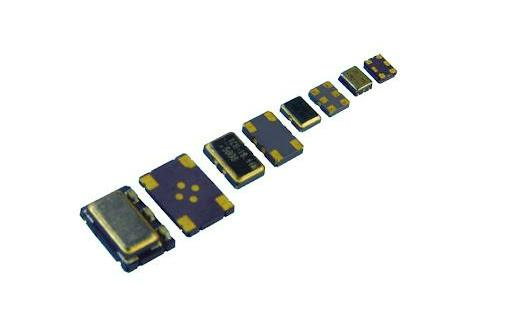
Ultra-small XC08M4 (1008) crystal oscillator, the perfect combination of performance and miniaturization
XC08M4 (1008) is suitable for 5G communication, Internet of Things, Wi-Fi, Bluetooth, smart wearable, space-constrained miniaturized products and other application scenarios, providing stable frequency support for high-density circuit boards.
0 notes
Text
Information required for IC-ID certification:
1. Circuit block diagram (including crystal vibration position, oscillation frequency)
2. Circuit diagram
3. Job description of the circuit
4. Instructions for use
5. Antenna gain
6. Applicant contact person, position, E-MAIL, applicant code click to download the application form
7. Canadian agent contact person, position, contact information
0 notes
Text
Principles of anti-interference design for printed circuit boards
Principles of anti-interference design for printed circuit boards
Layout of power cord:
1. According to the current size, try to widen the wire routing as much as possible.
2. The direction of power and ground wires should be consistent with the direction of data transmission.
3. A decoupling capacitor of 10-100 μ F should be connected to the power input terminal of the printed circuit board.
Layout of secondary ground wire:
1. Separate digital from analog.
2. The grounding wire should be thickened as much as possible, and at least 3 times the allowable current on the printed board should be passed, generally up to 2-3mm.
3. The grounding wire should form a dead loop as much as possible, which can reduce the potential difference of the grounding wire.
Three decoupling capacitor configuration:
1. The input end of the printed circuit board power supply is connected to an electrolytic capacitor with a temperature of 10-100 μ F. It would be even better if it could be greater than 100 μ F.
2. A 0.01~0.1 μ F ceramic capacitor is connected across the VCC and GND of each integrated chip. If space does not allow, a 1-10 μ F tantalum capacitor can be configured for every 4-10 chips.
3. Devices with weak anti noise capabilities and large changes in turn off current, as well as ROM and RAM, should have capacitors indirectly decoupled at VCC and GND.
4. Install a 0.01 μ F decoupling capacitor on the reset terminal "RESET" of the microcontroller.
5. The lead wires of decoupling capacitors should not be too long, especially for high-frequency bypass capacitors that cannot have leads.
Four component configuration:
1. The clock input terminals of the clock generator, crystal oscillator, and CPU should be as close and far away from other low-frequency devices as possible.
2. Try to keep low current circuits and high current circuits as far away from logic circuits as possible.
3. The position and orientation of the printed circuit board in the chassis should ensure that the components with high heat generation are located above.
Separate the wiring of five power lines, AC lines, and signal lines
Power lines and AC lines should be arranged on boards different from signal lines as much as possible, otherwise they should be routed separately from signal lines.
Six other principles:
1. Adding a pull-up resistor of around 10K to the bus is beneficial for anti-interference.
2. When wiring, try to have all address lines of the same length and as short as possible.
3. The lines on both sides of the PCB board should be arranged vertically as much as possible to prevent mutual interference.
4. The size of the decoupling capacitor is generally taken as C=1/F, where F is the data transmission frequency.
5. Unused pins can be connected to VCC through pull-up resistors (around 10K) or connected in parallel with the used pins.
6. Heating components (such as high-power resistors) should avoid devices that are easily affected by temperature (such as electrolytic capacitors).
7. Using full decoding has stronger anti-interference ability than line decoding.
To suppress the interference of high-power devices on the digital element circuits of microcontrollers and the interference of digital circuits on analog circuits, a high-frequency choke loop is used when connecting the digital ground to the common ground point. This is a cylindrical ferrite magnetic material with several holes in the axial direction. A thicker copper wire is passed through the holes and wound one or two times. This device can be regarded as having zero impedance for low-frequency signals and as an inductor for high-frequency signal interference Due to the high DC resistance of inductors, they cannot be used as high-frequency chokes
When signal lines outside the printed circuit board are connected, shielded cables are usually used. For high-frequency and digital signals, both ends of the shielded cable should be grounded. For low-frequency analog signals, it is better to ground one end of the shielded cable.
Circuits that are highly sensitive to noise and interference, or circuits with particularly severe high-frequency noise, should be shielded with a metal cover. The effect of ferromagnetic shielding on high-frequency noise at 500KHz is not significant, while the shielding effect of thin copper skin is better. When fixing the shielding cover with screws, attention should be paid to the corrosion caused by the potential difference when different materials come into contact
Seven good decoupling capacitors
The decoupling capacitor between the power supply and ground of an integrated circuit has two functions: on the one hand, it serves as the energy storage capacitor of the integrated circuit, and on the other hand, it bypasses the high-frequency noise of the device. The typical decoupling capacitance value in digital circuits is 0.1 μ F. The typical value of the distributed inductance of this capacitor is 5 �� H. A 0.1 μ F decoupling capacitor has a distributed inductance of 5 μ H, and its parallel resonance frequency is approximately 7MHz. This means that it has a good decoupling effect on noise below 10MHz and almost no effect on noise above 40MHz.
Capacitors with 1 μ F and 10 μ F have a parallel resonance frequency above 20MHz, which results in better removal of high-frequency noise.
Every 10 or so integrated circuits require the addition of one charging and discharging capacitor, or one energy storage capacitor, with an optional range of around 10 μ F. It is best not to use electrolytic capacitors. Electrolytic capacitors are made by rolling two layers of thin film together, and this rolled up structure appears as inductance at high frequencies. Use tantalum capacitors or polycarbonate capacitors.
The selection of decoupling capacitors is not strict, and can be based on C=1/F, that is, 0.1 μ F for 10MHz and 0.01 μ F for 100MHz.
When welding, the pins of the decoupling capacitor should be as short as possible, as long pins can cause the decoupling capacitor to self resonate. For example, when the pin length of a 1000pF ceramic capacitor is 6.3mm, the self resonant frequency is about 35MHz, and when the pin length is 12.6mm, it is 32MHz.
Eight experiences in reducing noise and electromagnetic interference
Principles of anti-interference design for printed circuit boards
1. The method of connecting resistors in series can be used to reduce the jumping rate of the upper and lower edges of the control circuit.
2. Try to make the potential around the clock signal circuit approach zero, circle the clock area with a ground wire, and keep the clock line as short as possible.
3. The I/O driver circuit should be located as close as possible to the edge of the printed board.
4. Do not hang the output terminal of the unused gate circuit, and the positive input terminal of the unused operational amplifier should be grounded, and the negative input terminal should be connected to the output terminal.
5. Try to use 45 ° polylines instead of 90 ° polylines for wiring to reduce the transmission and coupling of high-frequency signals to the outside world.
6. The clock line perpendicular to the I/O line has less interference than parallel to the I/O line.
6. The pins of the components should be as short as possible.
8. Do not trace wires under the quartz crystal oscillator and under components that are particularly sensitive to noise.
9. Do not form a current loop around the ground wire of weak signal circuits and low-frequency circuits.
10. When necessary, add ferrite high-frequency choke coils to the circuit to separate signals, noise, power, and ground.
A via on the printed circuit board causes a capacitance of approximately 0.6pF; The packaging material of an integrated circuit itself causes a distributed capacitance of 2pF~10pF; A connector on a circuit board with a distributed inductance of 520 μ H; A dual in-line 24 pin integrated circuit socket with a distributed inductance of 4 μ H~18 μ H.
Layout of power cord:
1. According to the current size, try to widen the wire routing as much as possible.
2. The direction of power and ground wires should be consistent with the direction of data transmission.
3. A decoupling capacitor of 10-100 μ F should be connected to the power input terminal of the printed circuit board.
Layout of secondary ground wire:
1. Separate digital from analog.
2. The grounding wire should be thickened as much as possible, and at least 3 times the allowable current on the printed board should be passed, generally up to 2-3mm.
3. The grounding wire should form a dead loop as much as possible, which can reduce the potential difference of the grounding wire.
Three decoupling capacitor configuration:
1. The input end of the printed circuit board power supply is connected to an electrolytic capacitor with a temperature of 10-100 μ F. It would be even better if it could be greater than 100 μ F.
2. A 0.01~0.1 μ F ceramic capacitor is connected across the VCC and GND of each integrated chip. If space does not allow, a 1-10 μ F tantalum capacitor can be configured for every 4-10 chips.
3. Devices with weak anti noise capabilities and large changes in turn off current, as well as ROM and RAM, should have capacitors indirectly decoupled at VCC and GND.
4. Install a 0.01 μ F decoupling capacitor on the reset terminal "RESET" of the microcontroller.
5. The lead wires of decoupling capacitors should not be too long, especially for high-frequency bypass capacitors that cannot have leads.
Four component configuration:
1. The clock input terminals of the clock generator, crystal oscillator, and CPU should be as close and far away from other low-frequency devices as possible.
2. Try to keep low current circuits and high current circuits as far away from logic circuits as possible.
3. The position and orientation of the printed circuit board in the chassis should ensure that the components with high heat generation are located above.
Separate the wiring of five power lines, AC lines, and signal lines
Power lines and AC lines should be arranged on boards different from signal lines as much as possible, otherwise they should be routed separately from signal lines.
Six other principles:
1. Adding a pull-up resistor of around 10K to the bus is beneficial for anti-interference.
2. When wiring, try to have all address lines of the same length and as short as possible.
3. The lines on both sides of the PCB board should be arranged vertically as much as possible to prevent mutual interference.
4. The size of the decoupling capacitor is generally taken as C=1/F, where F is the data transmission frequency.
5. Unused pins can be connected to VCC through pull-up resistors (around 10K) or connected in parallel with the used pins.
6. Heating components (such as high-power resistors) should avoid devices that are easily affected by temperature (such as electrolytic capacitors).
7. Using full decoding has stronger anti-interference ability than line decoding.
To suppress the interference of high-power devices on the digital element circuits of microcontrollers and the interference of digital circuits on analog circuits, a high-frequency choke loop is used when connecting the digital ground to the common ground point. This is a cylindrical ferrite magnetic material with several holes in the axial direction. A thicker copper wire is passed through the holes and wound one or two times. This device can be regarded as having zero impedance for low-frequency signals and as an inductor for high-frequency signal interference Due to the high DC resistance of inductors, they cannot be used as high-frequency chokes
When signal lines outside the printed circuit board are connected, shielded cables are usually used. For high-frequency and digital signals, both ends of the shielded cable should be grounded. For low-frequency analog signals, it is better to ground one end of the shielded cable.
Circuits that are highly sensitive to noise and interference, or circuits with particularly severe high-frequency noise, should be shielded with a metal cover. The effect of ferromagnetic shielding on high-frequency noise at 500KHz is not significant, while the shielding effect of thin copper skin is better. When fixing the shielding cover with screws, attention should be paid to the corrosion caused by the potential difference when different materials come into contact
Seven good decoupling capacitors
The decoupling capacitor between the power supply and ground of an integrated circuit has two functions: on the one hand, it serves as the energy storage capacitor of the integrated circuit, and on the other hand, it bypasses the high-frequency noise of the device. The typical decoupling capacitance value in digital circuits is 0.1 μ F. The typical value of the distributed inductance of this capacitor is 5 μ H. A decoupling capacitor with 0.1 μ F has a distributed inductance of 5 μ H, and its parallel resonance frequency is approximately 7MHz. This means that it has a good decoupling effect on noise below 10MHz and almost no effect on noise above 40MHz.
Capacitors with 1 μ F and 10 μ F have a parallel resonance frequency above 20MHz, which results in better removal of high-frequency noise.
Every 10 or so integrated circuits require the addition of one charging and discharging capacitor, or one energy storage capacitor, with an optional range of around 10 μ F. It is best not to use electrolytic capacitors. Electrolytic capacitors are made by rolling two layers of thin film together, and this rolled up structure appears as inductance at high frequencies. Use tantalum capacitors or polycarbonate capacitors.
The selection of decoupling capacitors is not strict, and can be based on C=1/F, that is, 0.1 μ F for 10MHz and 0.01 μ F for 100MHz.
When welding, the pins of the decoupling capacitor should be as short as possible, as long pins can cause the decoupling capacitor to self resonate. For example, when the pin length of a 1000pF ceramic capacitor is 6.3mm, the self resonant frequency is about 35MHz, and when the pin length is 12.6mm, it is 32MHz.
Eight experiences in reducing noise and electromagnetic interference
Principles of anti-interference design for printed circuit boards
1. The method of connecting resistors in series can be used to reduce the jumping rate of the upper and lower edges of the control circuit.
2. Try to make the potential around the clock signal circuit approach zero, circle the clock area with a ground wire, and keep the clock line as short as possible.
3. The I/O driver circuit should be located as close as possible to the edge of the printed board.
4. Do not hang the output terminal of the unused gate circuit, and the positive input terminal of the unused operational amplifier should be grounded, and the negative input terminal should be connected to the output terminal.
5. Try to use 45 ° polylines instead of 90 ° polylines for wiring to reduce the transmission and coupling of high-frequency signals to the outside world.
6. The clock line perpendicular to the I/O line has less interference than parallel to the I/O line.
6. The pins of the components should be as short as possible.
8. Do not trace wires under the quartz crystal oscillator and under components that are particularly sensitive to noise.
9. Do not form a current loop around the ground wire of weak signal circuits and low-frequency circuits.
10. When necessary, add ferrite high-frequency choke coils to the circuit to separate signals, noise, power, and ground.
A via on the printed circuit board causes a capacitance of approximately 0.6pF; The packaging material of an integrated circuit itself causes a distributed capacitance of 2pF~10pF; A connector on a circuit board with a distributed inductance of 520 μ H; A dual in-line 24 pin integrated circuit socket with a distributed inductance of 4 μ H~18 μ H.
Anti interference design of digital circuits and microcontrollers
In electronic system design, in order to avoid detours and save time, it is necessary to fully consider and meet the requirements of anti-interference, and avoid errors
After the design is completed, proceed with anti-interference remedial measures. There are three basic elements that form interference:
(1) Interference source refers to the components, equipment or signals that generate interference, described in mathematical language as follows: du/dt, di/dt is large ground
Fang is the source of interference. For example, lightning, relays, thyristors, motors, high-frequency clocks, etc. can all become sources of interference.
(2) The propagation path refers to the pathway or medium through which interference propagates from the interference source to the sensitive device. The typical interference propagation path is through
The conduction of wires and radiation in space.
(3) Sensitive devices refer to objects that are easily disturbed. For example: A/D, D/A converters, microcontrollers, digital ICs, weak signal amplifiers
Equipment, etc.
The basic principle of anti-interference design is to suppress interference sources, cut off interference propagation paths, and improve the anti-interference performance of sensitive devices.
(Similar to the prevention of infectious diseases)
1. Suppress interference sources
Suppressing interference sources means minimizing their du/dt and di/dt as much as possible. This is the top priority and most important principle in anti-interference design, often achieving twice the result with half the effort. Reducing the du/dt of the interference source is mainly achieved by paralleling capacitors at both ends of the interference source. Reducing the di/dt of the interference source is achieved by connecting an inductor or resistor in series with the interference source circuit and adding a freewheeling diode.
The common measures to suppress interference sources are as follows:
(1) Add a freewheeling diode to the relay coil to eliminate the back electromotive force interference generated when the coil is disconnected. Adding only a freewheeling diode will cause a delay in the disconnection time of the relay, while adding a voltage regulator diode will allow the relay to operate more times per unit time.
(2) Connect a spark suppression circuit (usually an RC series circuit, with a resistance of several K to tens of K and a capacitance of 0.01uF) in parallel at both ends of the relay contact to reduce the impact of electric sparks.
(3) Add a filtering circuit to the motor, paying attention to keeping the capacitor and inductor leads as short as possible.
(4) Each IC on the circuit board should be connected in parallel with a high-frequency capacitor of 0.01 μ F to 0.1 μ F to reduce the impact of the IC on the power supply. Pay attention to the wiring of high-frequency capacitors. The connection should be close to the power supply end and as thick and short as possible. Otherwise, it will increase the equivalent series resistance of the capacitor, which will affect the filtering effect.
(5) Avoid 90 degree creases during wiring to reduce high-frequency noise emissions.
(6) Connect RC suppression circuit at both ends of the thyristor to reduce the noise generated by the thyristor (which may cause breakdown of the thyristor in severe cases).
According to the propagation path of interference, it can be divided into two categories: conducted interference and radiated interference.
The so-called conducted interference refers to the interference that propagates through wires to sensitive devices. The frequency bands of high-frequency interference noise and useful signals are different, which can be cut off by adding filters on the wires to cut off the propagation of high-frequency interference noise. Sometimes, isolation optocouplers can also be added to solve the problem. The harm of power noise is the greatest, and special attention should be paid to handling it. The so-called radiation interference refers to the interference that propagates to sensitive devices through space radiation. The general solution is to increase the distance between the interference source and the sensitive device, isolate them with a ground wire, and add a shield on the sensitive device.
The common measures to cut off the interference propagation path are as follows:
(1) Fully consider the impact of power supply on the microcontroller. If the power supply is done well, the anti-interference of the entire circuit is solved by half. Many microcontrollers are sensitive to power noise, and it is necessary to add filtering circuits or voltage regulators to the microcontroller power supply to reduce the interference of power noise on the microcontroller. For example, a π - shaped filtering circuit can be composed of magnetic beads and capacitors. Of course, when conditions are not high, a 100 Ω resistor can also be used instead of magnetic beads.
(2) If the I/O port of the microcontroller is used to control noisy devices such as motors, isolation should be added between the I/O port and the noise source (by adding a π - shaped filtering circuit). Control noise components such as motors, and isolate them between the I/O port and the noise source by adding a π - shaped filtering circuit.
(3) Pay attention to the crystal oscillator wiring. The crystal oscillator and microcontroller pins should be as close as possible, and the clock area should be isolated with a ground wire. The crystal oscillator housing should be grounded and fixed. This measure can solve many difficult problems.
(4) Reasonable partitioning of circuit boards, such as strong and weak signals, digital and analog signals. Try to keep interference sources (such as motors and relays) as far away as possible from sensitive components (such as microcontrollers).
(5) Isolate the digital area from the analog area with a ground wire, separate the digital ground from the analog ground, and finally connect to the power ground at one point. The wiring of A/D and D/A chips is also based on this principle, and the manufacturer has considered this requirement when allocating the pin arrangement of A/D and D/A chips.
(6) The ground wires of microcontrollers and high-power devices should be separately grounded to reduce mutual interference. High power devices should be placed at the edge of the circuit board as much as possible.
(7) The use of anti-interference components such as magnetic beads, magnetic rings, power filters, and shielding covers in key areas such as microcontroller I/O ports, power lines, and circuit board connection lines can significantly improve the anti-interference performance of the circuit.
3. Improve the anti-interference performance of sensitive devices
Improving the anti-interference performance of sensitive devices refers to minimizing the picking up of interference noise from the perspective of sensitive devices, as well as methods for recovering from abnormal states as soon as possible.
The common measures to improve the anti-interference performance of sensitive devices are as follows:
(1) When wiring, try to minimize the area of the loop to reduce induced noise.
(2) When wiring, the power and ground wires should be as thick as possible. In addition to reducing pressure drop, it is more important to reduce coupling noise.
(3) For idle I/O ports of microcontrollers, do not hang them in the air. They should be grounded or powered on. The idle terminals of other ICs can be grounded or powered on without changing the system logic.
(4) The use of power monitoring and watchdog circuits for microcontrollers, such as IMP809, IMP706, IMP813, X25043, X25045, etc., can significantly improve the anti-interference performance of the entire circuit.
(5) On the premise that the speed can meet the requirements, try to reduce the crystal oscillator of the microcontroller and choose low-speed digital circuits as much as possible.
(6) IC devices should be soldered directly onto the circuit board as much as possible, with less use of IC sockets.
Let me first share my experience in this area:
In terms of software:
1. I am used to clearing all unused code space to "0" because it is equivalent to NOP and can be reset when the program runs away;
2. Add a few NOPs before the jump instruction, with the same purpose of 1;
3. When there is no hardware WatchDog, software simulation of WatchDog can be used to monitor the operation of the program;
4. When dealing with the adjustment or setting of external device parameters, in order to prevent errors caused by interference, the parameters can be resent at regular intervals, which can help the external devices recover as soon as possible;
5. Anti interference in communication can be achieved by adding data check bits and adopting a 3-to-2 or 5-to-3 strategy;
6. When there are communication lines, such as I ^ 2C and three wire systems, we have found that setting the Data line, CLK line, and INH line to high normally results in better anti-interference performance than setting them to low.
In terms of hardware:
1. The grounding and power lines are definitely important!
2. The disconnection of the route;
3. Separation of numbers and models;
4. Each digital component requires a 104 capacitor between ground and power supply;
5. In applications with relays, especially at high currents, to prevent interference from relay contact sparks on the circuit, a 104 and diode can be connected between the relay coils, and a 472 capacitor can be indirectly connected between the contacts and the starting point. The effect is good!
6. To prevent crosstalk between I/O ports, I/O ports can be isolated using methods such as diode isolation, gate circuit isolation, optocoupler isolation, electromagnetic isolation, etc;
7. Of course, the anti-interference ability of multi-layer panels is definitely better than that of single panels, but the cost is several times higher.
8. Choosing a device with strong anti-interference ability is more effective than any other method, and I think this should be the most important point. Because the inherent shortcomings of devices are difficult to compensate for through external methods, but often those with strong anti-interference ability are more expensive, while those with poor anti-interference ability are cheaper, just like Taiwan's Dongdong is cheap but its performance is greatly reduced! It mainly depends on your application scenarios
Printed circuit board (PC8) is a supporting component for circuit components and devices in electronic products. It provides electrical connections between circuit components and devices. With the rapid development of electrical technology, the density of PGB is getting higher and higher. The quality of PCB design has a significant impact on its anti-interference ability. Therefore, when designing PCBs, it is necessary to follow the general principles of PCB design and meet the requirements of anti-interference design.
0 notes
Text
Understanding Embedded Computing Systems and their Role in the Modern World
Embedded systems are specialized computer systems designed to perform dedicated functions within larger mechanical or electrical systems. Unlike general-purpose computers like laptops and desktop PCs, embedded systems are designed to operate on specific tasks and are not easily reprogrammable for other uses. Embedded System Hardware At the core of any embedded system is a microcontroller or microprocessor chip that acts as the processing brain. This chip contains the CPU along with RAM, ROM, I/O ports and other components integrated onto a single chip. Peripherals like sensors, displays, network ports etc. are connected to the microcontroller through its input/output ports. Embedded systems also contain supporting hardware like power supply circuits, timing crystal oscillators etc. Operating Systems for Embedded Devices While general purpose computers run full featured operating systems like Windows, Linux or MacOS, embedded systems commonly use specialized Real Time Operating Systems (RTOS). RTOS are lean and efficient kernels optimized for real-time processing with minimal overhead. Popular RTOS include FreeRTOS, QNX, VxWorks etc. Some simple devices run without an OS, accessing hardware directly via initialization code. Programming Embedded Systems Embedded Computing System are programmed using low level languages like C and C++ for maximum efficiency and control over hardware. Assembler language is also used in some applications. Programmers need expertise in Microcontroller architecture, peripherals, memory management etc. Tools include compilers, linkers, simulators and debuggers tailored for embedded development. Applications of Embedded Computing Embedded systems have revolutionized various industries by bringing intelligence and connectivity to everyday devices. Some key application areas include: Get more insights on Embedded Computing
Unlock More Insights—Explore the Report in the Language You Prefer
French
German
Italian
Russian
Japanese
Chinese
Korean
Portuguese
Alice Mutum is a seasoned senior content editor at Coherent Market Insights, leveraging extensive expertise gained from her previous role as a content writer. With seven years in content development, Alice masterfully employs SEO best practices and cutting-edge digital marketing strategies to craft high-ranking, impactful content. As an editor, she meticulously ensures flawless grammar and punctuation, precise data accuracy, and perfect alignment with audience needs in every research report. Alice's dedication to excellence and her strategic approach to content make her an invaluable asset in the world of market insights.
(LinkedIn: www.linkedin.com/in/alice-mutum-3b247b137 )
#Embedded Computing#Embedded Systems#Microcontrollers#Embedded Software#Iot#Embedded Hardware#Embedded Programming#Edge Computing#Embedded Applications#Industrial Automation
0 notes
Text
Unlocking the Potential of Quartz Powder in Manufacturing
Quartz powder, a finely ground form of crystalline silica, is an essential industrial material used in various sectors such as glass manufacturing, electronics, ceramics, construction, and more. It is highly valued for its physical and chemical properties, including durability, high melting point, low electrical conductivity, and resistance to wear. Industries across the globe are reliant on high-quality Quartz Powder Manufacturers to create products ranging from everyday household items to advanced technological components.
When it comes to sourcing premium-grade quartz powder, Sudarshan Group has established itself as a leading manufacturer and supplier in the market. With decades of experience and a commitment to innovation, Sudarshan Group has become a name synonymous with quality and reliability in the mineral industry. In this article, we will explore the importance of quartz powder, its applications, and why Sudarshan Group stands out among quartz powder manufacturers.
What is Quartz Powder?
Quartz powder is derived from natural quartz, a mineral composed primarily of silicon dioxide (SiO2). It is abundant in the Earth’s crust and occurs in a variety of forms, including large crystals, sand, and finely ground powder. Quartz has exceptional hardness, chemical stability, and optical properties, making it ideal for use in multiple industrial applications.
The process of creating quartz powder typically involves mining quartz deposits, crushing the raw material, and then grinding it to the desired particle size. High-purity quartz powder, which has fewer impurities such as iron and other trace minerals, is often used in specialized applications, especially in electronics and high-tech industries.
Applications of Quartz Powder
Glass Manufacturing: One of the most well-known applications of quartz powder is in the glass industry. Quartz is a key ingredient in the production of glass, contributing to the material’s strength, transparency, and resistance to high temperatures. The silica content in quartz powder acts as a flux, lowering the melting point of the raw materials used in glassmaking. This allows for the production of various types of glass, including soda-lime glass, borosilicate glass, and specialty glass used in laboratory equipment and optics.
Ceramics: In the ceramics industry, quartz powder is used as a filler material to enhance the mechanical strength of the final product. It helps improve the thermal shock resistance and overall durability of ceramic items, making them suitable for use in high-temperature environments. The fine particle size of quartz powder also ensures a smooth surface finish for ceramics, contributing to their aesthetic appeal.
Construction: Quartz powder is widely used in the construction industry, particularly in the production of concrete and mortar. The addition of quartz powder improves the strength, durability, and weather resistance of these materials, making them ideal for building structures that need to withstand harsh environmental conditions. In addition, quartz is used in engineered stone products, such as countertops and flooring, which combine beauty with practicality.
Electronics: High-purity quartz powder plays a critical role in the electronics industry. It is used in the production of semiconductors, integrated circuits, and solar cells due to its excellent electrical insulation properties. Quartz also has piezoelectric properties, meaning it can generate an electrical charge when subjected to mechanical stress. This makes it an essential component in devices like oscillators, sensors, and watches.
Paints and Coatings: In the paints and coatings industry, quartz powder is used as a filler material to improve the durability, gloss, and resistance of paints. It helps create coatings that are resistant to chemicals, heat, and wear, making them suitable for use in harsh environments. Quartz powder also enhances the adhesion of paint to surfaces, ensuring a long-lasting finish.
Foundry and Refractory Applications: Quartz powder is used in foundries to create molds for casting metals. Its high melting point and resistance to thermal expansion make it ideal for producing molds that can withstand extreme temperatures. In refractory applications, quartz powder is used to create heat-resistant materials that are essential for lining furnaces, kilns, and other high-temperature processing equipment.
Leading the Way in Quartz Powder Manufacturing
As one of the foremost quartz powder manufacturers, Sudarshan Group has a proven track record of providing high-quality quartz products to clients across various industries. Established with a mission to supply premium-grade minerals, Sudarshan has become a trusted name in the field of industrial minerals, especially quartz powder.
Commitment to Quality
Sudarshan Group prides itself on delivering quartz powder that meets the highest standards of purity and consistency. The company uses state-of-the-art technology in its mining and processing operations to ensure that the final product is free from impurities and has the desired particle size distribution. This commitment to quality is what sets it apart from other manufacturers.
The company also adheres to strict quality control measures throughout the production process, ensuring that every batch of quartz powder meets the specifications required by its clients. Whether it’s for glass manufacturing, electronics, or construction, Sudarshan quartz powder is designed to meet the demanding requirements of various industries.
Conclusion
Quartz powder is a versatile and essential material in a wide range of industries, from glass manufacturing to electronics and construction. As demand for high-quality quartz products continues to grow, manufacturers like Sudarshan Group play a crucial role in meeting this need. With a commitment to quality, sustainability, and customer satisfaction, it has earned its reputation as a leading quartz powder manufacturer. Whether you’re in the market for quartz powder for industrial or technological applications, it is a trusted partner that can deliver the products and support you need.
0 notes
Text
Get Arduino Atmega 2560 R3 Board at Affordable Price in Ainow

With the MAX3421e IC, the Mega 2560 Atmega2560-16au compatible with Arduino is a microcontroller board based on the Arduino Atmega 2560 R3.
With a total of 54 digital input/output pins (including 15 PWM outputs), 16 analog inputs, and 4 UARTs, the MEGA ADK is jam-packed with features. It also boasts a 16 MHz crystal oscillator and comes equipped with a USB connection, power jack, ICSP header, and reset button. Based on the Arduino Atmega 2560 r3, this board shares many similarities with its counterparts, including the ATmega8U2 program that serves as a USB-to-serial converter. In fact, the Mega ADK revision 3 even includes a resistor that conveniently pulls the 8U2 HWB line to ground for easier DFU(Device Firmware Upgrade) mode access.
New features on the board include:
As part of the 1.0 pin-out, the shields will be able to adjust to the voltage provided by the board by adding SDA and SCL pins near the AREF pin and two new pins near the RESET pin, the IOREF. Shields in the future will be compatible with boards that use AVR, which operate at 5V, and Arduino Due, which operates at 3.3V. The second pin, which is not connected, will be used for future purposes.
Circuit with a stronger RESET.
A USB connection or an external power supply can be used to power the Arduino Atmega 2560 R3 Android Accessory Development Kit (ADK). An AC-to-DC adapter (wall-wart) or battery can be used to supply external (non-USB) power. An adapter can be connected by plugging a 2.1mm center-positive plug into the board’s power jack.
GND and Vin pin headers on the POWER connector can be inserted with battery leads. Since the Mega R3 Android Accessory Development Kit (ADK) is a USB Host, the phone will attempt to draw power from it when it needs to charge. When the ADK is powered over USB, 500mA is available for the phone and board.
Features and specifications:
Arduino Atmega 2560 r3 :
Atmel is the programmer
Microcontroller ATmega2560.
A total of 54 digital input/output terminals (14 of which have programmable PWM outputs) are available.
There are 16 analog inputs.
There are four UARTs (hardware serial ports).
A crystal clock with a frequency of -16 MHz.
A bootloader allows sketches to be downloaded via USB without having to go through an external writer.
-Powered by USB or external power supply (not supplied). The device will automatically switch between power sources.
A heavy gold plate construction is used.
The clock speed is 16 MHZ.
Bootloader uses 8 KB of the 256 KB flash memory.
The operating voltage is 6 x 12 volts.
Mega 2560 Arduino cable:
It is hot pluggable.
-Compatible with PCs.
Strain relief and PVC overmolding ensure error-free data transmissions for a lifetime.
-Aluminum under-mold shield helps meet FCC requirements for KMI/RFI interference.
-Filled and braided shield conforms to fully rated cable specifications and reduces EMI/FRI interference.
Error-free, high-performance transmission.
Case made of transparent acrylic:
MEGA2560 R3 (unassembled) compatible.
It is possible to adjust the cover.
Transparent color.
Acrylic is the material used.
The power of
The external power regulator has a maximum capacity of 1500mA. Of this, 750mA is reserved for the phone and MEGA ADK board, while the remaining 750mA is dedicated to any attached actuators and sensors. To use this amount of current, a power supply must be able to provide at least 1.5A. While the board can run on an external supply ranging from 5.5 to 16 volts, it is recommended to use between 7 and 12 volts. If supplied with less than 7V, there may be insufficient voltage output from the 5V pin, potentially causing instability in the board. On the other hand, using more than 12V may result in overheating of the voltage regulator and potential damage to the board components.
What follows is:
This pin is used to supply voltage to the Arduino board when it is powered by an external power source rather than 5 volts from the USB connection or another regulated source.
This pin generates a regulated 5V from the board’s regulator. The board can be powered via the DC power jack (7-12V), USB connector (5V), or VIN pin (7-12V). If you supply voltage via the 5V or 3.3V pins, you bypass the regulator and can damage your board. Please do not do so.
The onboard regulator generates 3.3 volts. Maximum current draw is 50 milliamps.
The ground pins are GND.
The Arduino board’s IOREF pin serves as a voltage reference for the microcontroller. In a properly configured shield, you can determine the voltage of the IOREF pin and select an appropriate power source or enable voltage translators to work with either 5V or 3.3V outputs.
The memory
It has 256 KB of flash memory for storing code (of which 8 KB is used for the bootloader), 8 KB of SRAM, and 4 KB of EEPROM (which can be read and written).
The inputs and outputs
By using pin Mode(), digital Write(), and digital Read() functions, each of the Arduino Atmega 2560 R3 Android Accessory Development Kit (ADK)’s 50 digital pins can be used as inputs or outputs. There is an internal pull-up resistor of 20-50 Ohm on each pin. They operate at 5 volts. They can provide or receive a maximum current of 40 mA. Some of the pins have specialized functions:
Serial 0: 0 (RX) and 1 (TX), Serial 1: 19 (RX) and 18 (TX), Serial 2: 17 (RX) and 16 (TX), Serial 3: 15 (RX) and 14 (TX). Connected to the ATmega8U2 USB-to-TTL Serial chip on pins 0 and 1.
External Interrupts: 2 (interrupt 0), 3 (interrupt 1), 18 (interrupt 5), 19 (interrupt 4), 20 (interrupt 3), and 21 (interrupt 2). An interrupt can be triggered on a low value, a rising or falling edge, or a change in value using the attach Interrupt() function.
Providing 8-bit PWM output with the analog Write() function for PWM values 2 to 13 and 44 to 46.
SPI: 50 (MISO), 51 (MOSI), 52 (SCK), 53 (SS). These pins support SPI communication using the SPI library. They are also broken out on the ICSP header, which is physically compatible with Uno, Duemilanove, and Diecimila.
MAX3421E is the USB host.
The Max3421E
The following pins are used to communicate with Arduino via the SPI bus:
Seven (RST), fifty (MISO), fifty one (MOSI), and fifty two (SCK) are digital.
You should not use Digital pin 7 for inputs or outputs because it is used to communicate with MAX3421E
PJ3 (GP_MAX), PJ6 (INT_MAX), PH7 (SS) are not broken out on headers.
A built-in LED is connected to digital pin 13. When the pin is HIGH, the LED is on, when it is LOW, it is off.
Supports TWI communication using the Wire library. These pins are not in the same location as the Duemilanove or Diecimila TWI pins.
Android Accessory Development Kit (ADK) with Arduino Atmega 2560 R3 has 16 analog inputs, each with a resolution of 10 bits (i.e. 1024 different values). It is possible to change the upper end of the range of the pins by using the AREF pin and analog Reference() function. Other pins on the board include:
Reference voltage for analog inputs. Use with analog reference.
Reset. This line is typically used to add a reset button to shields which block the board’s reset button.
The communication process
The Arduino Atmega 2560 R3 Android Accessory Development Kit (ADK) offers various communication options, including connecting with a computer, another Arduino, or other micro-controllers. The ATmega2560 has four hardware UARTs for TTL (5V) serial communication. Additionally, the board has an ATmega8U2 that uses USB to provide a virtual com port for computer software. For Windows machines, a .inf file may be needed but OSX and Linux machines will automatically detect the board as a COM port. In the Arduino software, there is a serial monitor feature for sending and receiving simple textual data from the board.
When data is transmitted via the ATmega8U2/16U2 chip and USB connection to the computer (but not for serial communication on pins 0 and 1), the board’s RX and TX LEDs flash. Any of the MEGA ADK’s digital pins can be serialized with a software-serial library. TWI and SPI communication are also supported by the ATmega2560. The Arduino software contains a Wire library to simplify TWI communication, see Wire library for details. For SPI communication, use the SPI library.
The USB host interface given by MAX3421E IC allows Arduino MEGA ADK to connect and interact with any type of device with a USB port. It allows you to interact with many types of phones, control Canon cameras, and interface with keyboards, mice, and gaming controllers such as Wiimote and PlayStation 3.
The programming language
For details, see the reference and tutorials. You can program the Mega R3 Android Accessory Development Kit (ADK) with Arduino software (download). You don’t need an external hardware programmer to upload new code to the ATmega2560 on the MEGA ADK since it comes preburned with a boot-loader (just like the Arduino Atmega 2560 r3). The STK500v2 protocol (references and C header files) is used for communication.
You can also bypass the bootloader and program the microcontroller through the ICSP (In-Circuit Serial Programming) header using Arduino ISP or similar; see these instructions for details. Atmega8U2 firmware source code is available in the Arduino repository. An ATmega8U2 is loaded with a DFU bootloader, which can be activated by:
The Rev1 boards have the following features:
Resetting the 8U2 requires connecting the solder jumper on the back of the board (near the map of Italy).
Rev2 and later boards have a resistor pulling the 8U2/16U2 HWB line to ground, making it easier to put into DFU mode. To load a new firmware, you can use the FLIP software (Windows) or the DFU programmer (Mac OS X and Linux). If you prefer, you can use the ISP header with an external programmer (overwriting the DFU bootloader). See this user-contributed tutorial for more information.
Reset (automatic) software
The Arduino Atmega 2560 r3 ADK has been designed to reset by software from a connected computer instead of requiring a physical press of the reset button before an upload. This is achieved by connecting one of the hardware flow control lines (DTR) of the ATmega8U2 to the reset line of the ATmega2560 through a 100 nano-farad capacitor. Whenever this line is asserted, causing it to drop low, the chip will be reset momentarily. The upload button in the Arduino environment makes use of this feature, enabling you to easily upload code without needing to manually press the reset button.
As a result, the boot-loader’s timeout can be reduced since DTR can be synchronized with the upload initiation. This arrangement also has additional effects when the MEGA ADK is linked to a computer running Mac OS X or Linux. Upon being connected to software via USB, the board resets and enters bootloader mode for about half a second. During this time, any non-code data will be disregarded by the programmed bootloader, but it will capture the first few bytes of data transmitted after the connection is established.
Ensure that the software your sketch is communicating with allows for a brief pause after establishing the connection before sending any initial data. The MEGA ADK has a trace that can be removed to disable the auto-reset function. Connect the pads on either side of the trace to re-enable it, labeled as RESET-EN. Alternatively, you can disable the auto-reset by connecting a 110-ohm resistor from 5V to the reset line; additional information can be found in this forum thread.
Over-current protection for USB devices
A resettable polyfuse protects your computer’s USB ports from shorts and overcurrents with the Arduino Atmega 2560 R3 Android Accessory Development Kit (ADK). In spite of the fact that most computers have their own internal protection, a fuse provides an additional layer of protection. When more than 500 mA is applied to the USB port, the fuse automatically stops the connection.
Shield compatibility and physical characteristics
The Mega R3 Android Accessory Development Kit (ADK) PCB has a maximum length and width of 4 inches and 2.1 inches respectively. The USB connector and power jack extend beyond the length, while three screw holes are available for surface or case attachment. It is important to note that the distance between digital pins 7 and 8 is 160 mil, which is not an even multiple of the standard 100 mil spacing for the other pins. Additionally, the MEGA ADK can be used with most shields designed for the Uno, Diecimila or Duemilanove boards.
The digital pins 0 to 13 (as well as the adjacent AREF and GND pins), analog inputs 0 to 5, the power header, and the ICSP header are all positioned in the same spot. In addition, the main UART (serial port) is located on the same pins (0 and 1); as are external interrupts 0 and 1 (pins 2 and 3). SPI is also available through the ICSP header on the MEGA ADK and Duemilanove / Diecimila.
On the MEGA ADK (20 and 21), I2C and D are not located on the same pins.
1 note
·
View note