#Heterostructures
Explore tagged Tumblr posts
Visit Tumblr Blog
Explore Tumblr blogs with no restrictions, modern design and the best experience.
Last Seen Tumblr Blogs


Fun Fact
Tumblr has been providing a Korean-language service since 2013.
Text
Spin-to-Charge Conversion Without Magnetic Electrodes
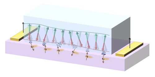
Measurements reveal the physical processes occurring where a magnetic insulator and few-layer graphene abut each other. [...] A central goal of spintronics is to create and manipulate spin-polarized currents. Typically, spintronic devices rely on magnetic electrodes for spin injection. However, a graphene–antiferromagnet interface could potentially offer a more efficient and energy-saving way to control current, functioning like an electrostatic gate. Theorists have predicted that magnons—collective spin excitations in a material—could couple to electrons at this interface, thereby mediating electron transport. Now Sujan Maity of the Indian Association for the Cultivation of Science and his colleagues have measured the predicted electron–magnon coupling [1]. The interaction at the interface allows for direct spin-to-charge conversion without the need for magnetic electrodes.
Read more.
#Materials Science#Science#Spintronics#Graphene#Interfaces#Antiferromagnetism#2D materials#Heterostructures
9 notes
·
View notes
Text
Famous Atheists
Zhores Ivanovich Alferov (1930-2019)

He contributed substantially to the creation of modern heterostructure physics and electronics. He is an inventor of the heterotransistor and co-winner (with Herbert Kroemer and Jack Kilby) of the 2000 Nobel Prize in Physics.
#nobel prize#famous atheists#atheism#religion#famous scientists#physicist#famous people#physics#atheists
4 notes
·
View notes
Text
Postdoctoral Research Associate- Thin Film Synthesis and Characterization of Quantum Materials
Job title: Postdoctoral Research Associate- Thin Film Synthesis and Characterization of Quantum Materials Company: Oak Ridge National Laboratory Job description: , you will focus on the growth of thin film and heterostructure quantum materials utilizing molecular beam epitaxy, and probing the… thin film synthesis, ultrahigh vacuum techniques such as scanning tunneling microscopy and…
0 notes
Text
Pioneering Hybrid Anode Material Signals a New Era for Lithium-Ion Battery Technology

As global reliance on lithium-ion batteries intensifies—fueling everything from portable electronics to electric vehicles and renewable energy grids—the industry faces mounting pressure to deliver higher energy densities, faster charging, and longer operational lifespans. Meeting these demands requires not just incremental improvements, but bold innovation at the material level.
A research team led by Professor Jae-Min Oh (Dongguk University) and Professor Seung-Min Paek (Kyungpook National University) has made a significant leap forward. Their latest work, published in the Chemical Engineering Journal, unveils a sophisticated hybrid anode material with the potential to transform lithium-ion battery performance.
This new material is a hierarchical heterostructure, ingeniously combining reduced graphene oxide (rGO) and nickel-iron layered double hydroxides (NiFe-LDH). The synergy between these components is the key: rGO forms an efficient, conductive network for electron transport, while the nickel-iron-oxide elements enable rapid, high-capacity charge storage through a pseudocapacitive mechanism.
R&D Highlights:
🔹The team utilized a layer-by-layer self-assembly technique with polystyrene bead templates. Polystyrene beads were coated with graphene oxide (GO) and NiFe-LDH precursors, then removed to create a hollow sphere structure.
🔹A carefully controlled thermal process induced a phase change in NiFe-LDH, generating nanocrystalline nickel-iron oxide (NiFe₂O₄) and amorphous nickel oxide (a-NiO), while simultaneously reducing GO to rGO. The result: a robust, well-integrated composite (rGO/NiFe₂O₄/a-NiO) with enhanced conductivity and stability.
🔹The hollow architecture prevents direct contact between active nanoparticles and the electrolyte, improving the anode’s durability and cycling stability.
🔹Advanced characterization techniques, including X-ray diffraction and transmission electron microscopy, validated the material’s structure and integration.
🔹Electrochemical testing demonstrated a specific capacity of 1687.6 mA h g⁻¹ at 100 mA g⁻¹ after 580 cycles—outperforming conventional anode materials and showcasing excellent rate performance even at elevated charge/discharge rates.
This research was made possible through close interdisciplinary collaboration, enabling optimized design and performance. As Professor Oh notes, the future of energy storage lies in synergistic, multi-material systems rather than incremental component upgrades.
The implications are profound: within the next 5–10 years, we could see batteries that are lighter, smaller, longer-lasting, and faster-charging—benefiting both everyday consumers and the broader push for sustainable energy.
Let’s connect and discuss the future of energy storage!
#BatteryTechnology #LithiumIon #HybridMaterials #Nanotechnology #Graphene #EnergyStorage #Electrochemistry #Innovation #SustainableTech
0 notes
Text
Unconventional unidirectional magnetoresistance in heterostructures of a topological semimetal and a ferromagnet
Source: Nature
https://search.app/pNicd
0 notes
Text
Towards topological quantum computing using InAs-Al hybrid devices
8:00 am – 8:36 am
Presenter: Chetan Nayak (Microsoft)
The fusion of non-Abelian anyons is a fundamental operation in measurement-only topological quantum computation. In one-dimensional topological superconductors, fusion amounts to a determination of the shared fermion parity of Majorana zero modes. Here, we introduce a device architecture that is compatible with future tests of fusion rules. We implement a single-shot interferometric measurement of fermion parity in indium arsenide-aluminum heterostructures with a gate-defined superconducting nanowire . The interferometer is formed by tunnel-coupling the proximitized nanowire to quantum dots. The nanowire causes a state-dependent shift of these quantum dots' quantum capacitance of up to 1fF. Our quantum capacitance measurements show flux h/2e-periodic bimodality with a signal-to-noise ratio of 1 in 3.6 microseconds at optimal flux values. From the time traces of the quantum capacitance measurements, we extract a dwell time in the two associated states that is longer than 1ms at in-plane magnetic fields of approximately 2T. These measurements are discussed in terms of both topologically trivial and non-trivial origins. The large capacitance shift and long poisoning time enable a parity measurement with an assignment error probability of 1%.
0 notes
Text
Microsoft’s Majorana hype: Real proof or just marketing?
New Post has been published on https://thedigitalinsider.com/microsofts-majorana-hype-real-proof-or-just-marketing/
Microsoft’s Majorana hype: Real proof or just marketing?

Introduction: The quest for reliable qubits
Quantum computing faces a fundamental challenge: qubits, the basic units of quantum information, are notoriously fragile.
Conventional approaches, such as superconducting circuits and trapped ions, require intricate error-correction techniques to counteract decoherence. Microsoft has pursued an alternative path: Majorana-based topological qubits, which promise inherent noise resistance due to their non-local encoding of quantum information.
This idea, based on theoretical work from the late 1990s, suggests that quantum states encoded in Majorana zero modes (MZMs) could be immune to local noise, reducing the need for extensive error correction. Microsoft has invested two decades into developing these qubits, culminating in the recent “Majorana 1” prototype.
However, given past controversies and ongoing skepticism, the scientific community remains cautious in interpreting these results.
The scientific basis of Majorana-based qubits
Topological qubits derive their stability from the spatial separation of Majorana zero modes, which exist at the ends of specially engineered nanowires. These modes exhibit non-Abelian statistics, meaning their quantum state changes only through specific topological operations, rather than local perturbations. This property, in theory, makes Majorana qubits highly resistant to noise.
Microsoft’s approach involves constructing “tetrons,” pairs of Majorana zero modes that encode a single logical qubit through their collective parity state. Operations are performed using simple voltage pulses, which avoids the complex analog controls required for traditional superconducting qubits.
Additionally, digital measurement-based quantum computing is employed to correct errors passively. If successful, this design could lead to a scalable, error-resistant quantum architecture.
However, while the theoretical framework for Majorana qubits is robust, experimental verification has been challenging. Majorana zero modes do not occur naturally and must be engineered in materials like indium arsenide nanowires in proximity to superconductors.
Establishing that these states exist and behave as expected has proven difficult, leading to past controversies.
Historical controversies: The 2018 retraction
A major setback for Microsoft’s Majorana initiative occurred in 2018 when researchers, including Leo Kouwenhoven’s team at TU Delft (funded by Microsoft), published a Nature paper claiming to have observed quantized conductance signatures consistent with Majorana zero modes.
This was hailed as a breakthrough in topological quantum computing. However, by 2021, the paper was retracted after inconsistencies were found in data analysis. Independent replication attempts failed to observe the same results, and an internal investigation revealed that a key graph in the original paper had been selectively manipulated.
This event, dubbed the “Majorana Meltdown,” significantly damaged the credibility of Microsoft’s approach. It highlighted the challenge of distinguishing genuine Majorana modes from other quantum states that mimic their signatures due to material imperfections. Many physicists became skeptical, arguing that similar issues could undermine subsequent claims.
Experimental progress and remaining challenges
Despite the 2018 controversy, Microsoft and its collaborators have continued refining their approach. The recent announcement of the “Majorana 1” chip in 2025 presents experimental evidence supporting the feasibility of Majorana-based qubits.
Key advancements include:
Fabrication of “topoconductor” materials: Microsoft developed a new indium arsenide/aluminum heterostructure to reliably host Majorana zero modes.
Parity measurement success: The team demonstrated that they could measure the qubit’s parity (even vs. odd electron occupation) with 99% accuracy, a crucial validation step.
Increased parity lifetime: The qubit’s state exhibited stability over milliseconds, significantly surpassing superconducting qubits’ coherence times (which are typically in the microsecond range).
Digital control implementation: Unlike analog-tuned superconducting qubits, Majorana qubits can be manipulated with simple voltage pulses, theoretically enabling large-scale integration.
While these are important steps forward, the experiments have not yet demonstrated key quantum operations, such as two-qubit entanglement via non-Abelian braiding. Until this milestone is achieved, claims about the superiority of topological qubits remain speculative.
Comparison with other qubit technologies
To assess Microsoft’s claims, it is useful to compare Majorana qubits with existing quantum computing platforms:
Superconducting qubits (IBM, Google): These have demonstrated successful quantum error correction and multi-qubit entanglement but require extensive calibration and error correction. Fidelity levels for two-qubit gates currently range around 99.9%.
Trapped-ion qubits (IonQ, Quantinuum): These offer superior coherence times (seconds vs. microseconds for superconductors) but suffer from slow gate speeds and complex laser-based control.
Majorana-based qubits: Theoretically provide built-in error protection, reducing the need for extensive error correction. However, experimental validation is still in progress, and large-scale integration remains untested.
Microsoft has argued that Majorana qubits will enable a quantum computer with a million qubits on a single chip, a feat that conventional qubits struggle to achieve.
While this is an exciting possibility, many researchers caution that scaling challenges remain, especially given the extreme conditions (millikelvin temperatures, precise nanowire fabrication) required for Majorana qubits.
Despite recent progress, many physicists remain skeptical of Microsoft’s claims.
Key concerns include:
Lack of direct evidence for Majorana zero modes: While Microsoft’s 2025 Nature paper presents strong supporting data, the scientific community has yet to reach a consensus that Majorana modes have been definitively observed.
Alternative explanations for observed phenomena: Many experimental signatures attributed to Majorana states could be explained by disorder-induced states or other trivial effects in semiconductor-superconductor interfaces.
Unverified large-scale claims: Microsoft’s assertion that its approach will lead to fault-tolerant quantum computing “within years, not decades” is met with skepticism. Experts note that even the most advanced conventional quantum computers are still years away from practical applications, and scaling from an 8-qubit chip to a million-qubit processor is an enormous leap.
Comparison to competing approaches: Some argue that improvements in quantum error correction for superconducting and trapped-ion qubits may render topological qubits unnecessary by the time they are fully realized.
A Promising but unproven path
Microsoft’s Majorana-based qubits represent one of the most ambitious efforts in quantum computing. The theoretical promise of intrinsic error protection and simplified quantum control is compelling, and recent experiments provide encouraging evidence that topological qubits can be realized.
However, historical controversies, ongoing skepticism, and the lack of key demonstrations (such as two-qubit gates) mean that these qubits are not yet a proven alternative to existing technologies.
While Microsoft has made significant strides in overcoming past setbacks, their claims of imminent large-scale quantum computing should be met with caution.
The coming years will be critical in determining whether Majorana qubits will revolutionize quantum computing or remain an elegant but impractical idea. As independent verification and further experiments unfold, the scientific community will ultimately decide whether Microsoft’s bold bet pays off.
#2025#aluminum#analog#Analysis#applications#approach#architecture#Artificial Intelligence#challenge#chip#Collective#Community#comparison#computer#computers#computing#computing platforms#data#data analysis#Design#effects#electron#employed#event#experimental#Explained#Fabrication#Fault-tolerant quantum computing#framework#Fundamental
0 notes
Text
From CoPilot: "
A qubit, or quantum bit, is the fundamental unit of information in quantum computing, analogous to a bit in classical computing. Unlike classical bits, which can be either 0 or 1, qubits can exist in a superposition of states, meaning they can be both 0 and 1 simultaneously. This unique property allows quantum computers to perform complex calculations more efficiently than classical computers.
Here's a summary of key features of qubits:
Superposition: A qubit can represent both 0 and 1 at the same time.
Entanglement: Qubits can be entangled, meaning the state of one qubit can depend on the state of another, even if they are far apart.
Quantum Interference: The ability to combine and manipulate quantum states, enabling more powerful computations.
Quantum computing harnesses these features to solve problems that are currently intractable for classical computers. The field is rapidly evolving, with ongoing research and development to make quantum computers more practical and scalable"
0 notes
Text
A pathway toward new quantum devices: Electrically defined quantum dots in zinc oxide https://phys.org/news/2024-11-pathway-quantum-devices-electrically-dots.html
0 notes
Text
"Optimizing Metal Ion Sensing Using ML" #sciencefather #machinelearning #researcher
This study introduces a machine learning (ML) framework for optimizing photodetector performance in metal ion sensing applications. The proposed system leverages a heterostructure of nitrogen-doped graphene quantum dots (N-GQDs) and gold nanoparticles (Au@N-GQDs). Over 20 supervised ML models were trained and evaluated to identify the most effective algorithm for detecting metal ions.
0 notes
Text
Researchers advance substrate engineering pathways to improve power electronics
As the growth in global electricity need and supply continues to accelerate, efficient power electronics will be key to improving grid efficiency, stability, integration, and resilience for all energy sources. Advances in wide-bandgap materials for semiconductors offer the potential to enable greater power handling in power electronics while reducing electrical and thermal losses. Wide-bandgap materials also allow for smaller, faster, more reliable, and more energy-efficient power electronic components than current commercial silicon-based power electronic components. Researchers from the National Renewable Energy Laboratory (NREL), the Colorado School of Mines, and Oak Ridge National Laboratory examined a potential route to achieve peak performance of aluminum gallium nitride, AlxGa1-xN, a key material for increasing power electronics' energy efficiency and performance, through growth on optimized substrate materials.
Read more.
#Materials Science#Science#Electronics#Semiconductors#Aluminum gallium nitride#Aluminum#Gallium#Nitrides#Thin films#Tantalum carbide#Tantalum#Carbides#Heterostructures#Interfaces#Computational materials science
10 notes
·
View notes
Text
Quantum Well Competition
Once I saw you, I felt the specific valence of no longer having a position to rest in.
Maybe it was just the design of that specific nanometric infrastructure; too many unlike particles in too small a region.
Maybe it was my lowered excitation state; the background energy insufficient to escalate it.
Or maybe you were already residing in all the 1-dimensional wells wherein I could potentially rest; superposed in all the same outcomes as i was.
Maybe you were just dominating that heterostructure in a way that I probably have done in so many other wells; unknowingly making you feel less welcome inside them. All I can say for certain is that the experience did not tend well to my pre-existing restlessness.
When the song said: “you are the piece of me I wish I didn’t need,” I felt it like a dagger.
There were several daggers.
I’m just a momentary particle trying to disentangle instead of annihilate.
1 note
·
View note
Text
Postdoctoral Research Associate- Thin Film Synthesis and Characterization of Quantum Materials
Job title: Postdoctoral Research Associate- Thin Film Synthesis and Characterization of Quantum Materials Company: Oak Ridge National Laboratory Job description: , you will focus on the growth of thin film and heterostructure quantum materials utilizing molecular beam epitaxy, and probing the… thin film synthesis, ultrahigh vacuum techniques such as scanning tunneling microscopy and…
0 notes
Text
Effect of the underlayer on the elastic parameters of the CoFeB/MgO heterostructures
http://dlvr.it/TCd25r
0 notes
Text
(17) PhD, Postdoc and Academic Jobs at Radboud University in the Netherlands

Radboud University invites application for vacant (17) PhD, Postdoc and Academic Jobs Radboud University invites application for vacant PhD, Postdoc and Academic Positions, a public university with a strong focus on research located in Nijmegen, the Netherlands. Postdoctoral Researchers: Environmental Science, Hydrology, Socioeconomics, Toxicology or Ecology of Pollutants Job opportunity 0.8 – 1.0 FTE Gross monthly salary: € 3,226 – € 5,090 Faculty of Science Are you eager to learn how emission, fate and effects of pollutants (and the water, material and biomass flows that carry them) are related to the size of cities, catchments, organisms and communities? Then join the ERC Advanced Grant project ’The… PhD Candidates: Environmental Science, Hydrology, Socioeconomics, Toxicology or Ecology of Pollutants Job opportunity 0.8 – 1.0 FTE Gross monthly salary: € 2,770 – € 3,539 Faculty of Science Are you eager to learn how emission, fate, and effects of pollutants (and the water, material and biomass flows that carry them) are related to the size of cities, catchments, organisms, and communities? Then join the ERC Advanced Grant project “The… PhD Candidate: The Conceptual History of Ethics in Modern Arabic Job opportunity 1.0 FTE Gross monthly salary: € 2,770 – € 3,539 Faculty of Philosophy, Theology and Religious Studies Are you fascinated by the history of ideas in the Arab world? By how the Arabic language developed in the modern age? By its discourse on ethics and how it has affected society? In this funded PhD position, you will research the modern history of the… PhD Candidate: Biogeochemistry Job opportunity 1.0 FTE Gross monthly salary: € 2,770 – € 3,539 Faculty of Science Would you like to contribute to understanding the impact of climate change on nutrient dynamics in high-latitude marine environments? Do you thrive in the dynamic blend of fieldwork adventures, laboratory experiments and geochemical modelling? As a… Postdoctoral Researcher: Growing Cancer Organoids in Synthetic Matrices Job opportunity 1.0 FTE Gross monthly salary: € 3,226 – € 5,090 Faculty of Science Progress in cancer biology is hampered by the difficulty to grow them in a realistic environment. The best models currently available are 3D tumour organoids. They are typically grown in animal-derived basement membrane extracts, which suffer from… PhD Candidate: Effect of Online and Offline Marketing of Alcohol-free Beverages on the Drinking Behaviour of Young People Job opportunity 1.0 FTE Gross monthly salary: € 2,770 – € 3,539 Faculty of Social Sciences Are you passionate about becoming an expert in the unique research field focusing on alcohol-free beverages? Do you want to join an interdisciplinary team that includes members from academia, policy and practice? Are you excited to conduct research… PhD Candidate: Declarative Programming and the Internet of Things Job opportunity 1.0 FTE Gross monthly salary: € 2,770 – € 3,539 Faculty of Science Are you an aspiring computer scientist with a fascination for declarative programming, the Internet of Things or topics that intersect with this? Then join the Software Science group at the Institute for Computing and Information Sciences as a PhD… PhD Candidate in Condensed Matter Physics for the Synthesis of 2D Materials Job opportunity 1.0 FTE Gross monthly salary: € 2,770 – € 3,539 Faculty of Science The goal of this PhD project is to develop, build and operate a vacuum compatible exfoliation center for the creation of heterostructures constructed from reactive 2D materials. PhD candidate Metaphysics and Philosophical Anthropology Job opportunity 1.0 FTE Gross monthly salary: € 2,770 – € 3,539 Faculty of Philosophy, Theology and Religious Studies Are you a creative and independant thinker who is passioned about German Philosophy? Are you interested in anthropological theories of the late 18th and early 19th centuries? And do you hold a Master’s degree in Philosophy, or are you close to… Assistant/Associate Professor of Chemistry Education Job opportunity 0.8 – 1.0 FTE Gross monthly salary: € 4,332 – € 8,025 Faculty of Science Are you an enthusiastic scientist in the field of chemistry education with a drive to work at the cutting edge of the field? Would you like to help us translate fundamental insights into engaging activities in teacher education? And are you willing… PhD Candidate: Philosophy of Science: Causal Inquiry in the Social Sciences Job opportunity 0.8 – 1.0 FTE Gross monthly salary: € 2,770 – € 3,539 Faculty of Philosophy, Theology and Religious Studies Are you a creative and independent thinker and passionate about analytic philosophy of science? Are you interested in exploring how social scientists uncover causes and effects in the social world? And do you hold (or are close to obtaining) a Master… PhD Candidate: International and European Law Job opportunity 1.0 FTE Faculty of Law Are you passionate about public international law? Do you aspire to carry out original and impactful research into contemporary international legal challenges? If so, you are invited to join the Department of International and European Law as a PhD… Assistant Professor: Exoplanets and their stellar environments Job opportunity 0.8 – 1.0 FTE Gross monthly salary: € 4,332 – € 5,929 Faculty of Science Are you an enthusiastic astrophysicist with a strong interest in exoplanets, particularly in relation to their parent stars? Would you like to share your expertise and contribute to our academic community? Then this exciting opportunity to join our… PhD Candidate: Experimental Approaches to Global Histories of Art and Architecture Job opportunity 1.0 FTE Gross monthly salary: € 2,770 – € 3,539 Faculty of Arts Are you an aspiring researcher in the field of art history, looking to start your academic career off right? Then become a PhD candidate at Radboud University and uncover unpublished and under-examined sources that can help us rethink existing… PhD Candidate: Computational Cognitive Neuroscience – Multisensory Perceptual Inference, Learning and Attention Job opportunity 1.0 FTE Gross monthly salary: € 2,770 – € 3,539 Faculty of Science We conduct weekly interim selections; therefore, we advise you to apply in a timely manner. The vacancy will close on August 1st or earlier if we find a suitable candidate before then. PhD Candidate: Computational Cognitive Neuroscience – Decision Confidence Job opportunity 1.0 FTE Gross monthly salary: € 2,770 – € 3,539 Faculty of Science We conduct weekly interim selections; therefore, we advise you to apply in a timely manner. The vacancy will close on August 1st or earlier if we find a suitable candidate before then. PhD Candidate: Apocalypticism in Contemporary Indigenous Literatures: Ways of Knowing the End of Times Job opportunity 0.8 – 1.0 FTE Gross monthly salary: € 2,770 – € 3,539 Faculty of Arts Today’s complex global questions require new scientific talents, whose fresh insights can shift the frontiers of research. As a PhD Candidate at Radboud University, you can become an expert in apocalypticism in contemporary Indigenous literatures. We… Read the full article
0 notes
Text
2D Devices: A Key to Keeping Quantum Computers Cool
There is great potential for revolutionising sectors such as drug discovery, artificial intelligence, and materials science with quantum computers. However, the requirement for extremely low temperatures is a considerable obstacle to their development. The basic building block of information in a quantum computer, known as a qubit, is extremely brittle and error-prone at even slightly higher temperatures. huge-scale quantum computers have historically been impractical due to the lack of access to these extremely cold settings, which has required the use of huge, energy-consuming dilution refrigerators.
Now for an innovative new development: 2D devices may be able to help cool quantum computers. Researchers at the Ecole Polytechnique Federale de Lausanne (EPFL) in Lausanne, Switzerland, created a gadget that converts heat into energy at temperatures below space. A smaller, more efficient cooling system could remove a major barrier to quantum computing development with this accomplishment.
The Quantum Computing Temperature Challenge
Quantum computers calculate via entanglement and superposition. Qubits must be delicate to deal with quantum information. This demands cold temperatures -273.15 degrees Celsius, or -459.67 degrees Fahrenheit often near absolute zero. Because thermal vibrations decrease, qubits stay stable and coherent longer at higher temperatures.
Maintaining such low temperatures is expensive, energy-intensive, and technically complex. Dilution refrigerators use various helium isotopes to cool. Because these systems are large and intricate, scaling quantum computers is an extremely difficult task.
2D devices Overview
Single-layer lattice materials like graphene, h-BN, and MoS2 are two-dimensional. These materials have different mechanical, thermal, and electrical properties than three-dimensional ones. The hexagonal lattice of carbon atoms in graphene gives it extraordinary electrical conductivity and strength.
Researchers have studied 2D devices in electronics, photonics, and energy storage. Due to their unique properties, quantum computing technologies benefit from them.
Thermal Control in Quantum Computing
Heat management is one of the most exciting uses of 2D devices in quantum computing. Metallic and semiconductor quantum computing materials can produce thermal noise and heat dissipation issues that influence qubit stability. Instead, 2D materials have many advantages.
High thermal conductivity: Graphene dissipates heat. This trait helps remove quantum processor heat, keeping qubit stability at low temperatures.
Diminished Electron-Phonon Interactions: In traditional materials, heat can be produced via the interaction of electrons with phonons, which are quantized crystal lattice vibrations. Because 2D devices have fewer electron-phonon interactions, they produce less heat and have better thermal management.
Electrical Insulation: A number of 2D devices, like h-BN, combine good electrical insulation with thermal conductivity. This combination can efficiently dissipate heat and help separate qubits from electrical noise.
Combining Quantum Devices with Two-Dimensional Materials
Several novel strategies are needed to incorporate 2D devices into quantum devices. To improve the performance and temperature control of quantum circuits, researchers are creating methods for fabricating and integrating two-dimensional materials.
Graphene-Based Cooling: One method for cooling quantum processors is to use graphene as a layer. Heat can be effectively transmitted away from the qubits by putting graphene layers in contact with the quantum devices, preserving the low temperatures necessary for their operation. Moreover, the strong electrical conductivity of graphene guarantees that it does not disrupt the quantum states of the qubits.
2D Heterostructures: Interfaces with specific qualities can be created by combining several 2D materials to generate heterostructures. For instance, graphene and h-BN together can offer superior electrical insulation and thermal management. Quantum devices can benefit from the integration of these heterostructures to improve their overall performance.
Phonon Engineering: Researchers can further minimise heat generation and thermal noise by manipulating the phonon characteristics of 2D devices. In order to reduce interactions with the quantum states of the qubits, this entails adjusting the vibrational modes of the materials.
Experimental Progress
Recent developments in experiments show that 2D materials have promise for use in quantum computing. For example, MIT researchers have created a way to add graphene to superconducting qubits, greatly enhancing their coherence times. The efficient heat dissipation of the graphene layers lowers thermal noise and prolongs the lifetime of the qubits in their quantum states.
Researchers at the University of California, Berkeley also looked into using h-BN as an insulating layer in quantum devices in another study. The findings demonstrated that h-BN effectively conducted heat away from the qubits, assisting in the maintenance of low temperatures in addition to offering superior electrical insulation.
Future challenges and prospects
2D materials in quantum computing have potential, but many challenges remain. One challenge is integrating these materials into quantum computing architectures. To guarantee compatibility and performance, new fabrication processes and techniques must be developed.
Furthermore, a detailed investigation is required into the long-term stability and scalability of quantum devices based on 2D materials. For these devices to be used in real applications, it is essential that they can function dependably for longer periods of time and can be scaled up for bigger quantum systems.
Prospective avenues for investigation could centre on investigating novel two-dimensional materials and their amalgamations to enhance the thermal and electrical characteristics for use in quantum computing. Furthermore, utilising 2D materials to their full potential in quantum technologies will depend heavily on developments in material science and nanofabrication methods.
Future Consequences for Quantum Computing
Some of the biggest obstacles facing the development of quantum computing may be solved by incorporating 2D materials into the devices. 2D materials can improve qubit performance and stability by lowering noise and managing heat better, opening the door to more dependable and scalable quantum computing.
Furthermore, previously unthinkable new kinds of quantum devices and architectures might be made possible by the special qualities of 2D materials. This could hasten the development of useful quantum technology by creating new opportunities for quantum computing research and innovation.
In summary
Two-dimensional materials present a viable resolution to the thermal management issues associated with quantum computing. Their distinct characteristics, such as elevated thermal conductivity and diminished electron-phonon interactions, provide them perfect options for enhancing the efficacy and durability of quantum devices. Even while incorporating these materials into current architectures still presents problems, current research and experimental advancements offer a solid platform for next innovations.
2D devices have a huge potential impact on quantum computing. These materials have the potential to be essential for achieving the full promise of quantum technologies, as they can facilitate more effective cooling and minimise thermal noise. The combination of 2D devices and quantum computing promises to open up new avenues for research and development in this industry, propelling the next wave of technological developments.
Read more on Govindhtech.com
#quatum#QuantumComputing#2ddevice#2Dmaterial#govindhtech#technologynews#technology#technologytrends#technews#news
0 notes