#Magnetron Sputtering Technology
Explore tagged Tumblr posts
Visit Tumblr Blog
Explore Tumblr blogs with no restrictions, modern design and the best experience.
Last Seen Tumblr Blogs


Fun Fact
12.7% of mobile users access Tumblr.
Text
Hybrid Micro Circuits
Explore HHV Advanced Tech's space-grade hybrid micro circuits, featuring superior thin film metallization through magnetron sputtering and electrical properties.
For more information visit our website: https://hhvadvancedtech.com/thin-films-and-optics/thin-films-and-optics/products/space/hybrid-micro-circuits

0 notes
Text

New semiconductor material AlYN promises more energy-efficient and powerful electronics
Researchers at Fraunhofer IAF have made a breakthrough in the field of semiconductor materials: With aluminum yttrium nitride (AlYN), they have succeeded in fabricating and characterizing a new and promising semiconductor material using the MOCVD process. Due to its excellent material properties and its adaptability to gallium nitride (GaN), AlYN has enormous potential for use in energy-efficient high-frequency and high-performance electronics for information and communications technology. Aluminum yttrium nitride (AlYN) has attracted the interest of many research groups around the world due to its outstanding material properties. However, the growth of the material has been a major challenge. Until now, AlYN could only be deposited by magnetron sputtering.
Read more.
#Materials Science#Science#Semiconductors#Electronics#Aluminum#Yttrium#Nitrides#Materials processing
17 notes
·
View notes
Text
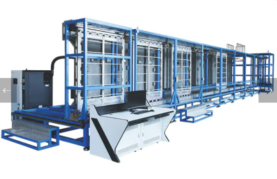
Magnetron Sputtering Coating Production Line
Continuous magnetron sputtering coating is an advanced thin film deposition technology that uses a magnetic field to control the movement trajectory of ion beams in a low-pressure environment, achieving sputtering adhesion to the material surface, thereby forming a uniform, dense, and well-adhered thin film layer on the substrate. This technology can not only improve the hardness, wear resistance, and corrosion resistance of materials but also alter their optical, electrical, and thermal properties to meet the needs of different fields.
0 notes
Text
0 notes
Text
Electron Beam Sources
Explore HHV Ltd's top-tier technology: Ion Beam, Thermal Evaporation, Electron-Beam, and Magnetron Sputtering systems designed to boost your projects with superior results.
For more information visit our website: https://hhvltd.com/technology
0 notes
Text
0 notes
Text
How Many Coating Methods are Available on the Surface of Optical Glass?
As a Glass Lab Manufacturer, share with you.
Coating is to coat a very thin transparent film on the surface to reduce light emission. There are many production methods for coated glass, mainly including vacuum magnetron sputtering method, vacuum evaporation method, chemical vapor deposition method and sol-gel method.

Optical Glass Blanks
1. Magnetron sputtering coated glass can design and manufacture multi-layer complex film system by using magnetron sputtering technology, which can plate a variety of colors on the white glass substrate. The film has good corrosion resistance and wear resistance, which is suitable for production. And one of the more used products.
2. There is a certain gap between the variety and quality of vacuum evaporation coated glass and magnetron sputtering coated glass, which has been gradually replaced by vacuum sputtering.
3. The chemical vapor deposition method is to introduce reaction gas into the float glass production line to decompose on the hot glass surface, and evenly deposit on the glass surface to form coated glass. The method is characterized by low equipment investment, easy control, low product cost, good chemical stability, and thermal processing. It is one of the more promising production methods.
4. The sol-gel method for producing coated glass has a simple process and good stability. The disadvantage is that the product's light transmittance is too high and the decoration is poor.
There are specific requirements for optical constants, and it has the characteristics of high transmission in the visible region and no selective absorption and coloring. According to the size of Abbe number, it is divided into coronal type and flint type glass, and each type is divided into several types according to the refractive index, and they are arranged in order according to the refractive index. Mostly used as lenses, prisms, mirrors, etc. of telescopes, microscopes, cameras, etc.
Our company also has Optical Glass Blanks on sale, welcome to contact us.
0 notes
Text

High-performance BWS sputtering system for advanced thin-film coatings
The BWS sputtering system is a state-of-the-art tool designed for precision thin-film deposition in research and industrial applications. Leveraging magnetron sputtering technology, this system ensures uniform and high-quality coatings on various substrates. With features like advanced process control, high throughput, and adaptability for multiple materials, the BWS sputtering system is ideal for applications in semiconductors, optics, and material science. Its robust design and user-friendly interface make it a reliable choice for achieving superior deposition results.
0 notes
Text
Physical Vapor Deposition Coating: Methods for the Future

What are the Physical Vapor Deposition coating approaches for the future? Ever wonder how the elegant, robust finishes on luxury timepieces, vehicle parts, and modern equipment are accomplished? Top Pvd coating Kerala is the novel solution. With unmatched benefits in terms of durability, appearance, and environmental impact, this revolutionary technology is changing the field of surface engineering.
Describe PVD Coating
A luxury living room furniture in Bangalore, Karnataka method known as physical vapor deposition (PVD) forms a thin film by vaporising solid components in a vacuum atmosphere and then laying them onto a substrate. Three primary steps—vaporization, transit, and condensation—form part of this process. High-energy sources evaporate the coating material, such as an electron beam, resistive heating, or arc discharge in a vacuum chamber.
Transportation: Maintaining its gaseous condition, the vaporized substance passes via the vacuum chamber.
Condensation: A thin, homogeneous coating results from the vapor condensing on the substrate.
Uses of PVD Coating
Industry of Automobile Equipment
PVD coatings spectrum Bangalore improves engine components, gear, and other important parts performance and longevity in the automotive industry. Better fuel economy and lower maintenance costs are achieved in part by PVD coatings' reduced friction and enhanced wear resistance.
Medical Objects
PVD coatings greatly help medical tools and implants since they are biocompatible and resistant to wear and corrosion. PVD-coated surgical instruments remain sharp and sterile for extended periods, guaranteeing accuracy and safety during medical treatments.
Watch Video: Click Here
Tool for Cutting
Custom-designed luxury furniture is essentially used in the machining sector as cutting tools. PVD-coated tools' reduced friction and enhanced hardness lead to higher cutting speeds, longer tool life, and better precision. For manufacturers, this lowers expenses and increases output.
Technology
Using protection, PVD coatings are applied in the electronics sector to improve the performance of parts, including semiconductors, sensors, and displays. PVD techniques' thin, homogeneous coatings guarantee great dependability and performance in electrical equipment.
The Prospect of PVD Coating
As long as research and development continue to stretch the boundaries of this technology, PVD coating looks bright. Innovations in coating materials development, deposition technique improvement, and PVD coating application expansion center on these areas.
Fresh Materials
Researchers are investigating novel materials to improve PVD coatings' qualities even more. Diamond-like carbon (DLC) coatings are under development for greater hardness and wear resistance. Such developments create fresh opportunities in sectors needing extremely durable surfaces.
Enhanced Techniques for Deposition
The development of deposition methods seeks to increase PVD process efficiency and cost-effectiveness. High-power impulse magnetron sputtering (HiPIMS) and other innovations enhance the quality and homogeneity of PVD coatings, increasing their availability for a greater spectrum of uses.
Broad Uses
As PVD coating technology develops, its uses should expand into new sectors. For example, PVD coatings on solar panels and wind turbine components would improve their efficiency and durability, benefiting the renewable energy sector.
Conclusion
With its unparalleled durability, cosmetic appeal, and environmental advantages, PVD coating transforms the surface engineering discipline. PVD coating will be very important as businesses seek creative ideas to enhance sustainability and product performance. PVD coating finds wide and always expanding uses in automotive, medical, electronics, and fashion. Accepting this new technology will surely result in a time when goods are more attractive and durable and better for our world.
Full Audio: Listen Here
Direction: Get Here
#pvd coating service bangalore#luxury sofa set for living room#luxury dining chairs#pvd coating bangalore#luxury sofa set#spectrum pvd coating#pvd decorative coatings#pvd coating price in bangalore#luxury leather sofa set
0 notes
Text

What is the difference between ceramic, high frequency and ordinary PCB boards?
Ceramic substrate is a kind of special PCB board with good thermal conductivity, insulation performance, and high dielectric constant. It is widely used in terminal products in the field of heat dissipation. Commonly used ceramic-based materials include aluminum oxide, aluminum nitride, zirconium oxide, ZTA, silicon nitride, silicon carbide, etc. FR circuit board refers to a circuit with epoxy glass fiber cloth as the main material. So, what is the difference between ceramic circuit board and ordinary PCB board
The difference between ceramic substrate and PCB board
Different materials. Ceramic substrate is an inorganic material, and the core is aluminum oxide or aluminum nitride; ordinary PCB board uses FR4 glass fiber board, which is an organic material. Ordinary PCB board can be laminated in multiple layers. LTCC is the mainstream of ceramic multilayer circuit board. The ceramic multilayer process currently being developed by Hitech Circuits Co., Ltd. is different from the traditional method. It uses magnetron sputtering technology to grow a layer of ceramic medium on the ceramic circuit board that has been metallized, and then re-metallizes this layer of medium to make the second layer of circuit.
b. The performance and application of ceramic substrates are different. The thermal conductivity of ceramic substrates far exceeds that of ordinary PCB boards. The thermal conductivity of alumina ceramics is ≧25W(m·K), and the thermal conductivity of aluminum nitride ceramics is ≧170W(m·K). They are used in industries with large heat dissipation requirements, such as high-power LED lighting, high-power modules, high-frequency communications, and track power supplies. The thermal expansion coefficient of ceramic substrates is more compatible with silicon wafers, and the product stability is higher. Ordinary PCB boards are widely used, mostly in private commercial products.
The difference between ceramic substrates and high-frequency boards
Different materials. Ceramic substrates are made of aluminum oxide or aluminum nitride, while high-frequency boards are mostly made of Rogers, Yalong, polytetrafluoroethylene, etc., with low dielectric constants and fast high-frequency communication speeds.
Different performance. Ceramic substrates are widely used in cooling sheets and systems, high-power modules, automotive electronics and other fields. High-frequency PCB boards are mainly used in high-frequency communications, aviation, high-end consumer electronics, etc.
3. In the field of high-frequency communications involving heat dissipation requirements, ceramic substrates are usually required to be combined with high-frequency PCB boards, such as high-frequency ceramic PCBs.
If you want to know ceramic PCBs, please feel freely to contact Cynthia at [email protected]
0 notes
Text
Better Neutron Mirrors Can Reveal the Inner Secrets of Matter - Technology Org
New Post has been published on https://thedigitalinsider.com/better-neutron-mirrors-can-reveal-the-inner-secrets-of-matter-technology-org/
Better Neutron Mirrors Can Reveal the Inner Secrets of Matter - Technology Org
Improved neutron mirrors can increase the efficiency of material analysis in neutron sources such as the ESS, which is being built outside Lund.
The improved mirror has been developed by researchers at Linköping University by coating a silicon plate with extremely thin layers of iron and silicon mixed with boron carbide. Their study has been published in the journal Science Advances.
Jens Birch, Fredrik Eriksson, Anton Zubayer and Naureen Gahfoor are some of the researcher behind the study now published in Science Advances. Image credit: Olov Planthaber/Linköping University
“Instead of increasing the power on the neutron source, which is extremely expensive, it’s better to focus on improving optics,” says Fredrik Eriksson, researcher at the Thin Film Physics Division at Linköping University.
Together with protons, neutrons form atomic nuclei. Depending on the number of neutrons in a nucleus, the properties of the element can differ. In addition, neutrons can also be used to analyse different materials at a very detailed level. This method is called neutron scattering.
Advanced materials science
Such measurements are carried out at special neutron research laboratories called neutron sources. One such laboratory, the European Spallation Source, or ESS, is now being built outside Lund. This is an investment of EUR 2 billion.
Fredrik Eriksson explain how the measurements of reflectivity works. Image credit: Olov Planthaber/Linköping University
The ESS and other neutron sources can be compared to advanced microscopes that allow scientists to investigate various materials and their properties down to the atomic level. They are used in everything from studying atomic structures, material dynamics and magnetism, to the functions of proteins.
It requires enormous amounts of energy for the neutrons to be released from the atomic nuclei. When the neutrons are released in the neutron source, they must be captured and directed toward their target, that is, the material to be investigated. Special mirrors are used to direct and polarise the neutrons. These are known as neutron optics.
Polarising optics
Although the ESS will have the world’s most powerful neutron source, the number of neutrons available in the experiments will be limited. To increase the number of neutrons that reach the instruments, improved polarising optics are required. This is something researchers from Linköping University have now achieved by improving neutron optics on several important points to increase efficiency.
“Our mirrors have better reflectance, which increases the number of neutrons that reach their target. The mirror can also polarise the neutrons into the same spin much better, which is important for polarised experiments”, says Anton Zubayer, doctoral student at the Department of Physics, Chemistry and Biology and lead author of the article published in Science Advances.
He continues:
“Also, as this no longer requires a large magnet, the mirror can be placed closer to the samples or other sensitive equipment without affecting the samples themselves, which in turn enables new types of experiments. In addition, we have also reduced the diffuse scattering, which means that we can reduce background noise in the measurements.”
High reflectivity
The mirrors are manufactured on a silicon substrate. Through a process called magnetron sputtering, it is possible to coat the substrate with selected elements. This process makes it possible to coat it with several thin films on top of each other, i.e. a multilayer film. In this case, iron and silicon films are used, mixed with isotopic enriched boron carbide. If the layer thicknesses are of the same order of magnitude as the neutron wavelength, and the interface between the layers is very smooth, the neutrons can exit the mirror in phase with each other, giving a high reflectivity.
Fredrik Eriksson believes that every neutron is precious and every small improvement in the efficiency of the neutron optics is valuable to improve the experiments.
“By increasing the number of neutrons and also reflecting higher neutron energies, opportunities are opened for pioneering experiments and groundbreaking discoveries across disciplines including physics, chemistry, biology and medicine,” says Fredrik Eriksson.
The study was funded by the Swedish Research Council, the Royal Swedish Academy of Engineering Sciences, the Royal Swedish Academy of Sciences, the Hans Werthén Foundation, the Knut and Alice Wallenberg Foundation, the Swedish Foundation for Strategic Research, and through the Swedish Government’s strategic investment in new functional materials, AFM, at Linköping University.
Facts: Neutron analysis makes use of the neutrons’ ability to behave both as a wave and as a particle. These neutrons, in turn, can have two different spins. It is important mainly for magnetic studies to be able to use polarised neutrons, i.e. neutrons with only one specific spin.
Article: Reflective, polarizing, and magnetically soft amorphous neutron optics with 11B-enriched B4C; Anton Zubayer, Naureen Ghafoor, Kristbjörg Anna Thórarinsdóttir, Sjoerd Stendahl, Artur Glavic, Jochen Stahn, Gyula Nagy, Grzegorz Greczynski, Matthias Schwartzkopf, Arnaud Le Febvrier, Per Eklund, Jens Birch, Fridrik Magnus, Fredrik Eriksson; Science Advances 2024 published online 14 February 2024. DOI: 10.1126/sciadv.adl0402
Written by Anders Törneholm
Source: Linköping University
You can offer your link to a page which is relevant to the topic of this post.
#2024#advanced materials#Analysis#Article#atomic#atomic nuclei#background#billion#Biology#chemistry#Chemistry & materials science news#Discoveries#dynamics#efficiency#energy#engineering#equipment#Facts#Featured physics news#form#Foundation#Fundamental physics news#Giving#Government#how#investment#iron#it#Link#magnet
0 notes
Text
Flexible Material Fiber Winding Vacuum Coating Equipment
Flexible material fiber winding coating equipment is a specialized device used for coating treatment on flexible materials. This type of equipment typically operates in a vacuum environment, using magnetron sputtering technology or other coating methods to prepare one or more functional thin films on the surface of flexible substrates. Here is a brief description of this device.

0 notes
Text
Butterfly-inspired films create vibrant colors while passively cooling objects
The new films, which don’t absorb any light, could be used on the outside of buildings, vehicles and equipment to reduce the energy needed for cooling while preserving vivid color properties. “In buildings, large amounts of energy are used for cooling and ventilation, and running the air conditioner in electric cars can reduce the driving range by more than half,” said research team leader Wanlin Wang from Shenzhen University in China. “Our cooling films could help advance energy sustainability and carbon neutrality.” In Optica, Optica Publishing Group’s journal for high-impact research, the researchers show that the films they developed lower the temperature of colorful objects to about 2 °C below the ambient temperature. They also found that when left outside all day, the blue version of the films was approximately 26°C cooler than traditional blue car paint. This represents an annual energy savings of approximately 1377 MJ/m2 per year. “With our new films, excellent cooling performance can be achieved, no matter the desired color, saturation or brightness,” said Wang. “They could even be used on textiles to create clothes of any color that are comfortable in hot temperatures.” Inspired by nature A car with blue paint appears blue because it absorbs yellow light and reflects blue light. The large amount of light that is absorbed heats the car. Morpho butterflies, however, produce their highly saturated blue color based on the nanostructure of their wings. The design of the cooling nanofilm mimics these structures to produce vibrant colors that don’t absorb light like traditional paint. advertisement To create their Morpho-inspired nanofilms, the researchers placed a disordered material (rough frosted glass) under a multilayer material made of titanium dioxide and aluminum dioxide. They then placed this structure on a silver layer that reflects all light, thus preventing the absorption of solar radiation and the heating associated with that absorption. The film’s color is determined by how components within its multilayered structure reflect light. To create blue, for example, the multilayer material is designed to reflect yellow light in a very narrow range of angles while the disordered structure diffuses the blue light across a broad area. Although this type of passive photonic thermal management has been accomplished before, it has only been used with white or clear objects because it is difficult to maintain a wide viewing angle and high color saturation. Passive cooling of colorful objects “Thanks to the layered structure we developed, we were able to extend the passive cooling method from colorless objects to colorful ones while preserving color performance,” said Wang. “In other words, our blue film looks blue across a large range of viewing angles and doesn’t heat up because it reflects all the light. In addition, high saturation and brightness can be achieved by optimizing the structure.” To test the new technology, the researchers created blue, yellow and colorless films, which they placed outdoors at Shenzhen University, on surfaces such as roofs, cars, cloth and cell phones, from 9 a.m. to 4 p.m. in both winter and summer. Using thermocouple sensors and infrared cameras to measure temperature, they found that the cooling films were more than about 15 ? cooler than the surfaces they were placed on in the winter and about 35 ? cooler in the summer. The researchers point out that replacing the silver film with an aluminum film would make the films less expensive and manufacturable by a scalable fabrication method such as electron beam evaporation and magnetron sputtering. Now that they have demonstrated the cooling and color performance of the films, the researchers plan to study and optimize other properties such as mechanical and chemical robustness.
0 notes
Text

Rostec enhances fighter canopy glass to improve stealth
Fernando Valduga By Fernando Valduga 03/29/22 - 4:00 PM in Military
Sukhoi Su-75 Checkmate. "Stealth" glass acquires special properties due to thin films of metals and metal oxides, deposited on its surface by magnetron spraying in a vacuum machine. (Photo: Rostec)
Sukhoi Su-75 Checkmate. "Stealth" glass acquires special properties due to thin films of metals and metal oxides, deposited on its surface by magnetron spraying in a vacuum machine. (Photo: Rostec)
Obninsk Research and Production Enterprise, a subsidiary of Rostec, has developed a new Su-57 fighter canopy glass to provide better stealth resources.
The design solution allows you to improve by 20% the characteristics of the cockpit windows of aviation complexes, including reducing the visibility of combat vehicles in radar range, Rostec said in a statement.
The special properties of stealth glass are given by the thinnest films of metals and metal oxides deposited on its surface by sputtering of magnetron in a vacuum installation. The configuration update increased the peak spray values of the magnetron by more than three times, making it possible to depose films with a much lower surface resistance. The engineering solution significantly improves the quality of the coating applied to aircraft glazing products in series, thanks to which the cockpit canopy receives improved optical characteristics and low radar visibility. These factors increase the combat potential and survivability of "stealth birds".

"Today, the samples produced with updated equipment have proven their characteristics calculated during measurements and tests. The new technology will be used to create structural optics for advanced aviation systems. This will reduce the radar signature of the aircraft and increase its combat capabilities," Rostec Vice President Vladimir Artyakov said, according to the press office.
ONPP Technologies has unique experience in the independent development and mass production of structural optics products with multifunctional thin film coatings applied. Today, the engineering and software solutions implemented by the company's experts allow you to create metal-optical structures composed of 200 or more layers, each with a thickness of 0.25–0.3 nm.
Tags: Military AviationROSTECRussiaStealth Technology (discretion)
Fernando Valduga
Aviation photographer and pilot since 1992, he has participated in several events and air operations, such as Cruzex, AirVenture, Dayton Airshow and FIDAE. He has works published in a specialized aviation magazine in Brazil and abroad. He uses Canon equipment during his photographic work in the world of aviation
Cavok Brasil - Digital Tchê Web Creation
9 notes
·
View notes
Text
Enhance Precision and Performance with a Custom Vacuum System from HHV Ltd

In the world of high-precision engineering, having the right tools and systems can make all the difference. Whether it’s for scientific research, semiconductor manufacturing, aerospace, or optical coating, the need for highly efficient vacuum systems has never been greater. At HHV Ltd, we specialize in designing and manufacturing advanced vacuum technologies tailored to meet the most demanding application requirements. A Custom Vacuum System from HHV Ltd not only ensures peak performance but also delivers reliability and control that off-the-shelf solutions often can’t match.
Why Choose a Custom Vacuum System?
Off-the-shelf vacuum systems may suit basic needs, but when it comes to advanced industrial or research applications, a one-size-fits-all solution often falls short. That’s where a Custom Vacuum System becomes a game-changer.
HHV Ltd brings decades of experience in developing tailored vacuum systems that align precisely with the operational, spatial, and technological demands of our clients. Our in-house team of engineers works closely with customers to analyze their requirements, select appropriate materials, and integrate compatible components to ensure seamless performance.
Whether you're working in thin-film deposition, space simulation, or material research, our custom systems offer a higher degree of process control, safety, and longevity. We incorporate modular designs, robust materials, and user-friendly interfaces, backed by global support services.
Key Features and Applications of HHV's Custom Vacuum Systems
Precision Engineering for High-Performance Applications
At HHV Ltd, we understand that precision is paramount. Our Custom Vacuum System designs are driven by performance metrics such as pressure stability, pump-down time, temperature control, and contamination resistance. These systems are widely used in:
Thin-film deposition for optics, solar cells, and semiconductors
Surface science and nanotechnology research
Aerospace and defense testing environments
Space simulation chambers for satellite component testing
Every system is rigorously tested and calibrated to ensure it meets the most stringent quality standards. With HHV’s expertise, customers gain access to advanced vacuum technologies that provide consistent results in even the most sensitive environments.
Tailored Solutions to Meet Unique Industry Needs
Each industry comes with its own set of technical challenges. HHV Ltd excels in customizing solutions that fit seamlessly into existing infrastructures or are built from the ground up. From chamber size and geometry to vacuum pumping systems and control software, every detail of our Custom Vacuum System is meticulously tailored.
Our systems also support integration with ancillary technologies like thermal evaporation units, magnetron sputtering sources, and cryo pumps. Clients benefit from enhanced operational flexibility, enabling them to run a wider range of experiments or production processes with a single system.
By leveraging our expertise and state-of-the-art manufacturing facility, HHV ensures that each system delivers optimal performance, minimal downtime, and long-term reliability.
Conclusion: Invest in Innovation with HHV Ltd
If your operations demand precision, reliability, and performance, investing in a Custom Vacuum System from HHV Ltd is a strategic choice. Our commitment to innovation and quality means you’ll receive a vacuum solution engineered for excellence and backed by decades of industry leadership.
For more insights, visit: https://hhvltd.com/
0 notes
Photo
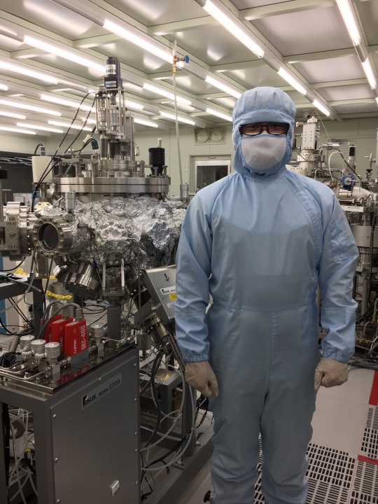

Meet Christian Laurio, materials scientist
1) What do you do? I am a doctoral student in Materials Science with research focusing on the strong coupling of an optical mode called Bloch surface waves (BSW) and exciton in photonic multilayer platforms. The strong coupling of light (photons) and matter (surface plasmons, phonons, excitons) leads to hybrid light-matter quasiparticles called polaritons. In my research, I perform numerical and experimental work to determine the influence of multilayer structural parameters (thickness, materials, etc) on the Rabi splitting, which is a measure of the strength of interaction, and polariton mode visibility. I simulate, fabricate, and characterize photonic multilayer structures and use spectroscopy to study the system. 2) Where do you work? I belong to the Quantum Materials Science Laboratory at the Nara Institute of Science and Technology in Nara, Japan. I perform all my research activities within the Division of Materials Science.
3) Tell us about the photos!
[Left:] This is me and my cleanroom buddy-- I often use it to fabricate my samples, an RF magnetron sputtering system.
[Right:] From my research visit at the University of Eastern Finland as part of my doctorate program. I spent two months in the beautiful city of Joensuu, where temperatures drop to as low as -30°C. It was a winter wonderland!
4) Tell us about your academic career path so far.
I graduated from the Valenzuela City Science High School (now Valenzuela City School of Mathematics and Science) and proceeded with my bachelor’s and master’s degrees in Physics at the Ateneo de Manila University. I am actually expecting to graduate this September and will move to the University of Bonn in Germany for a postdoc position.
5) Anything else you’d like to share?
Studying and living in Japan is a great experience. Although language barrier can be a problem (especially for me who didn’t have enough motivation to really learn Japanese), luckily there are many Filipinos and other international students at my university.
11 notes
·
View notes