#RF module types
Explore tagged Tumblr posts
Visit Tumblr Blog
Explore Tumblr blogs with no restrictions, modern design and the best experience.
Last Seen Tumblr Blogs


Fun Fact
The most popular pages on Tumblr are about Minecraft, GIFs, and David J. Peterson.
Text
0 notes
Text


Twin Famicom
NES with internal Disk system from Sharp
The Twin Famicom is a video game console system that was produced by Sharp Corporation in 1986 (Juli 1) and was only released in Japan. It is a licensed Nintendo product that combines the Famicom (NES) and the Famicom Disk System into a single piece of hardware.
The essential parts of the Twin Famicom include a 60-pin socket for Famicom cartridges and a socket for Disk System disks. The player could switch between the two media types with a switch – cassette "カセット" or disk "ディスク" The Twin Famicom is fully compatible with the NES and can handle accessories made for the NES (e.g. Beam Gun). But there is also an extra port on the Twin Famicom. This allows a 'regular' Famicom to use the Twin Famicom's disk drive.
The original Famicom only has one color combination, and the Twin Famicom was initially sold in two colors: red with black highlights (AN-500R), and black with red highlights (AN-500B). A second version of the system was released in 1987 with a slightly different case design, turbo controllers, and two different color schemes; black with green highlights (AN-505-BK) and red with beige highlights (AN-505-RD).
Like the Famicom, the Twin Famicom uses NTSC but with an AV output rather than an RF modulator with an RCA connector for composite video and mono audio, allowing for greater audiovisual quality on TVs and monitors with such inputs. An external RF modulator is bundled with the unit for connection through a TV's antenna/cable input. The two gamepads are hardwired into the console, so they cannot be disconnected.
More info:
https://ultimatepopculture.fandom.com/wiki/Twin_Famicom
#nintendo#famicom#twin famicom#sharp#nintendo disk system#retrogaming#retro gaming#nes#retro computing#retrocomputing#80s#80s computer#japan only
19 notes
·
View notes
Text
Best Partner for Wireless Modules: A Comprehensive Antenna Selection Guide
n the field of wireless communication, antenna selection is crucial. It not only affects the coverage range and transmission quality of signals but also directly relates to the overall performance of the system. Among various wireless modules, finding the right antenna can maximize their potential, ensuring stable and efficient data transmission.
When designing wireless transceiver devices for RF systems, antenna design and selection are essential components. A high-quality antenna system can ensure optimal communication distances. Typically, the size of antennas of the same type is proportional to the wavelength of the RF signal; as signal strength increases, the number of required antennas also grows.
Antennae can be categorized as internal or external based on their installation location. Internal antennas are installed within the device, while external antennas are mounted outside.
In situations where space is limited or there are multiple frequency bands, antenna design becomes more complex. External antennas are usually standard products, allowing users to simply select the required frequency band without needing additional tuning, making them convenient and easy to use.
What are the main types of antennas?
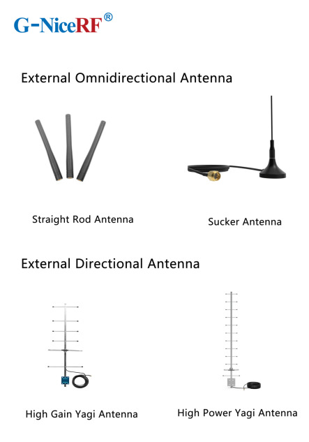
External Antennas: These antennas can be classified into omnidirectional antennas and directional antennas based on the radiation pattern.
Internal Antennas: These antennas refer to antennas that can be placed inside devices.
Omnidirectional Antennas: These antennas radiate signals uniformly in the horizontal plane, making them suitable for applications that require 360-degree coverage, such as home Wi-Fi routers and mobile devices.
Directional Antennas: These antennas have a high emission and reception strength in one or more specific directions, while the strength is minimal or zero in others. Directional antennas are primarily used to enhance signal strength and improve interference resistance.
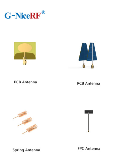
PCB Antennas: These antennas are directly printed on the circuit board and are suitable for devices with limited space, commonly used in small wireless modules and IoT devices.
FPC Antennas: FPC antennas are flexible printed circuit antennas that are lightweight, efficient, and easy to integrate.
Concealed Antennas: Designed for aesthetic purposes, concealed antennas can be hidden within devices or disguised as other objects, making them suitable for applications where appearance is important without compromising signal quality.
Antenna Selection Guide
When selecting the appropriate antenna for a communication module, it's essential to first determine whether to use an internal or external antenna based on the module's structure.
External Antennas: These antennas offer high gain, are less affected by the environment, and can save development time, but they may take up space and impact the product's aesthetics.
Internal Antennas: These have relatively high gain and are installed within the device, maintaining a clean and appealing exterior.
Sucker Antennas: These provide high gain and are easy to install and secure.
Copper Rod Sucker Antennas: Made from large-diameter pure copper radiators, these are highly efficient with a wide bandwidth.
Rubber Rod Antennas: Offer moderate gain at a low cost.
Fiberglass Antennas: Suitable for harsh environments and ideal for long-distance signal

External Directional Antennas
Typically used in environments with long communication distances, small signal coverage areas, and high target density.
Panel Antennas have high efficiency, are compact, and easy to install, while considering the impact of gain and radiation area Yagi Antennas offer very high gain, are slightly larger, and have strong directionality, making them suitable for long-distance signal transmission; however, attention must be paid to the antenna's orientation during use
Internal Antenna Selection
Most internal antennas are affected by environmental factors and may require custom design or impedance matching
Spring Antennas are cost-effective but have low gain and narrow bandwidth, often requiring tuning for good matching when installed Ceramic Patch Antennas occupy minimal space and perform well, but have a narrow bandwidth
For details, please click:https://www.nicerf.com/products/ Or click:https://nicerf.en.alibaba.com/productlist.html?spm=a2700.shop_index.88.4.1fec2b006JKUsd For consultation, please contact NiceRF (Email: [email protected]).
2 notes
·
View notes
Text
The SX1278 LoRa modules are used in Long Range communications. It is a type of low cost RF front-end transceiver module based on SX1278 from Semtech Corporation. The high sensitivity (-136dBm) in LoRa modulation and 20dBm high power output make the module suitable for low range and low data rate applications.
4 notes
·
View notes
Text
AM-Detection -the not easy way
Sometimes quite simple things can be a real nightmare if you take a closer look. One of those is AM detection. Your worst enemies are distortion and fading (the latter results in the first). The AM-Detector is only one little part in a receiver, exactly that kind of part usually no one thinks about. "It works, so what should be wrong with?" -a lot and sometimes there's more wrong than right.
A good part of that distinctive AM-Sound we all know is because of the Detector, even under the best conditions. If you're listen to shortwave or the broadcast band during the night then you also have to cope with Fading. Shouldn't be that problem, the automatic gain control takes care of that, right? Ehmmm... Yes. Sometimes. Why the sound gets so distorted when the signal goes down? Just because it's very often 'Selective Fading' and not just Fading -and your Detector doesn't like it.
Really good AM-Reception has a lot in common with High-End-Audio: if it shall work well EVERYTHING has to be well. So let's just talk a bit about Detectors...
Basically the Detector just splits the Audio Signal from the received and amplified Signal. Sounds easy and in fact it is -up to some degree. If you want more than this things getting complicated -really complicated. In at least 999 out of 1000 AM-Receivers for the Detector a small circuitry called 'Envelope Detector' is used, it's just a small Diode (Tube or Semiconductor), a few Resistors and small Capacitors. So, from the view of the Development Engineer: just put half a dozen cheap Components together and Bob's your Uncle. To tell the Truth: compared to the expense that thingy works surprisingly well. Because of this it's the 'Gold Standart' for this task since at least the mid 30s. But as good as it is, it absolutely has it's Limitations. Up to about 15...30% Distortion at a 100% Modulation Level is one, the inability to detect a signal with different sidebands (>selective Fading!) properly another.
To overcome these Limitations a thing named 'Synchronous Detector' was developed many Decades ago. This kind of Circuit has many advantages over the Envelope Detector, but to make one the complexity and the component count of those is just hilarious compared to the Envelope Detector. If only the result counts and nothing else: that's the way to go. We'll talking later how this exactly works, but before this you have to know that in a receiver with a Synchronous Detector also an Envelope Detector is needed: just for tuning in. So first we'll have a closer look how we can get the most ideal Envelope Detector.
Basically it's quite simple: want to have low overall Distortion? Feed it with at least 'a few' volts RF at it's input for having a high ratio between the input voltage and the 'forward voltage' of the Diode. Want low Distortion at low modulation levels? Use a Diode with low Impedance and a load Resistor with a value as low as possible. Want low Distortion at high modulation levels? Just make the input Impedance of the following Stage as high as possible for having the highest possible Ratio between the Resistance of the Load Resistor and the input Impedance of the following Stage.
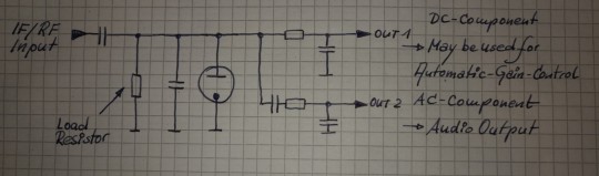
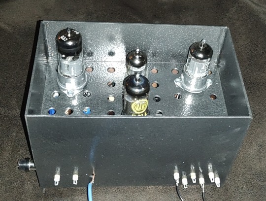
The Receiver i wanted to use (R+S EK07) has an IF output, meant for exactly such things, the IF Level there's about 250mVpp @ 300kHz. So having everything above in mind -and just adding a 700mVpp IF output for the Synchronous Detector and an additional AGC-Circuitry, then we're coming to this:

The EK07 is a fully tube equipped receiver, so i also want to use tubes as far as possible and -like in the EK07- in a way which guarantees 10k's of Service hours. If at one point a Semiconductor may perform muuuch better -ok, so then. First of all i want high performance. So what tubes may perform optimal here?
For the first IF-Amp (IF1) not much is needed, the Gain is only about 3, the output voltage low and besides that it has to be an remote-controlled type. Selectivity isn't needed or desired, so no IF-Can, only a Broad-Band setup. Nearly every IF-Tube with a Transconductance of at least about 3000mhos (3mA/V) would do that job. To have better performance i took the EF805s, which is a Special Quality Version of the EF85 -or 6BY7.
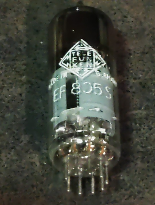
Transconductance is about twice what's needed, so we'll have Gain to spare, anyway, it's getting controlled with the AGC so it will work with less current which adds greatly to the service life. So no problems here.
For the second IF-Amp (IF2), things aren't exactly that easy. First: the output for the Synchronous Detector is placed between both Amps and has to deliver a constant voltage, so for the 2nd IF we need an Amplifier with an fixed Gain. A STABLE fixed Gain over long time periods. Further we want to have a relatively high and undistorted output voltage which calls for quite a bit of gain. Wait: there was also that thing with the low-value Load Resistor in the detector itself -so we also need a quite reasonable amount of output power from this stage. In Addition we want to have a stable gain for a time as long as possible. A IF-Tube like the EF805s could also handle this, but then we have to 'beat the crap' out of this thing. Not a good start for a long and stable service life, also not with Special Quality Tubes.
Because of all that my choice was a kinda 'special'-Special-Quality type: the E81L.

The datasheet calls this a 'Long range, Special Quality Tube for the use in Telephone Equipment'. Telephone Equipment? Like an answering machine?? Nope, by far not. Back in these days telephone companies needed to have Amplifiers for pushing the calls through loooong cables for long range service. But: this was all multiplex service, so they pushed dozens and dozens of calls simultaneously through one pair of wires or a Coax. The same way like for cable TV. THIS was these bulbs were meant for. For this task every company employed tens of thousands of such tubes 24/7/365. If a single one failed -most likely somewhere in nowhere of course- they had a problem. So they absolutely had to last.
These little bulbs are designed for about 4.5W plate dissipation at 20mA, the Transconductance is 11000mhos (11mA/V)-so it's about twice an usual IF Tube in every respect. So that's exactly what's needed here: a tube especially designed to last, quite powerful, so we can drive it with comfortable low settings, enhancing service life and stability much further.
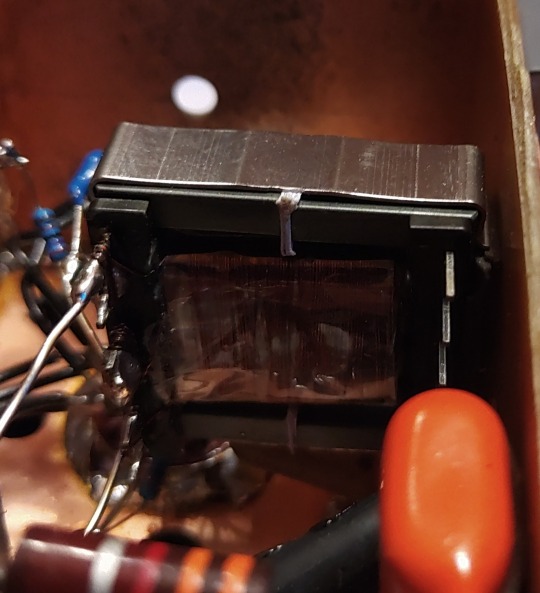
Because we need some amount of power the usual Broad-Band Amplifier arrangement (still: selectivity is not wanted or desired) with just a plate Resistor isn't good here, a suitable inductor works way better here. This has the further advantage that we can build it with a Tab like an Autotransformer -we don't need that much voltage it could deliver with that inductor by far, so this adds further to a good SNR and lower output Impedance. 300kHz trough a transformer? Yep, no problem. Just use the right core. Here it's not a laminated iron core but a ferrite one instead. Cause it's a single-A Amplifier of course we must add an air-gap, preventing saturation.
In a penthode stage the gain depends nearly exclusively on the Transconductance of the tube used, have to much just cut it down. The E81L has a quite high transconductance, about 3 times more than needed -and in the same order than big output tubes like the 6550, EL34 or 6CA7. For cutting that down to the desired level just put a Resistor or Pot in series to the bypass cap of the cathode Resistor. This acts as an series feedback so it also enhances linearity and long time stability greatly. Yap, i thought quite a while about which tube i should use here.
So after all Amplification is done now, we need a Diode for the Envelope Detector. Back in the Octal-Days this was the 6H6 / EB34, later in the Miniature-Days the 6AL5 / EAA91, both with two separate diodes in one bottle (or Can for the 6H6). These were not A DIODE, these were THE DIODE, so there's not much to choose from. Both are kinda close to each other, but are these ideal for what we want? They both can handle a reverse voltage of several hundreds of volts, so waaaay more than we need here. Both having a Plate Resistance of 600-something Ohms per System which is quite low -could be lower, even with both Systems in parallel. Of course these would be work well, no doubt about. But still.... Hey, this should be High-end so we're whining here at a very high level!
Basically we can use EVERY TUBE as a diode: just take the control grid as Anode, the Cathode as what it is and everything else as Shielding. We don't need hundreds of Volts reverse Voltage, nor high current, so also no big Cathode. We only want to have an internal Resistance as low as possible, so a close spacing between the Grid and the Cathode. This calls for a small Tube with a high Gm (or Transconductance) -like the 6AK5 / EF95. Can it handle the reverse voltage we need? Datasheet says 50V, so at least twice of what's needed. So just take one, put some current trough and take the voltage drop. Result: 210 ohms -way less than that what one of the double-diodes would provide, even with both Systems in parallel. Fits very well!

This is the soviet-military version of the 6AK5W / E95F. Special Quality. See these 'trenches' in the bulb? And the microscopic rivets holding the Plate together? The Soviets literally ruggedized the heck out of this tube! Why? Just because they used it widely in their Fighter Planes, ICBM's, Tanks and so on. Doubts about the soviet built quality? Hey, they wanted to win WWIII with them -so: nope. If you ever saw a ruggedized tube: this it is.
After the Detector itself is done, we come to last part of our little contraption: the buffer Amplifier. At the output of the Detector we have the AF as well with the overlayed AGC-Voltage and we want to have an input Impedance as high as possible for the Buffer Amp. Voltage Gain isn't needed -we have plenty of both from the Detector- so we just can use a Cathode Follower for the buffer. Ideally the Buffer should handle both voltages simultaneously, but then the output will be negative with respect to Ground. How to....? Simple: just put that thing between a positive and a negative supply rail. Then the output can swing freely between every positive or negative Potential as desired. Further: we don't need a Grid Resistor! The Grid just follows any voltage swing of the Detector, this also adds to a high input Impedance.
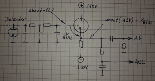
This Circuit will provide us a very high input Impedance, but this is High-End! So: what tube will be the best for? Because of the lack of any Grid Resistor the input Impedance depends now largely on the contact potential of the grid. So we want a tube with low contact potential which calls for a tube with a low Transconductance. Further we want a tube which needs only a low bias voltage for it's Grid, 'cause we'll loose any bias-volt in our AGC-Output voltage. This calls for a tube with an high Gain. Low contact potential and low Transconductance? High Gain?? That's the 12AX7 / ECC83! Ok, it's of course a double Triode, but we still can use the second system for something else -like for the Line-Output Amp. In that Stage there's not much needed so it also will perform well enough there -we're still talking about AM!
So let's put everything neatly together, adding adequate shielding and so on -and we get this:
So now it's time to have a closer look we did everything right. Just put a 300kHz-Carrier in, 100% modulated with a triangle-signal. We should get a perfect Triangle at the AF-Output -if physics are with us. Due to the Triangle Signal any Distortion can easily be spotted on the Scope.

Looks promising! But somehow... Is the beam defocused? Let's take a very close look:

No, it's not. Those are just the very small remnants of the Carrier, so we actually have a look how the Detector works on a nearly 'microscopic' Level. I could take a measurement how much distortion we have left, but the Flanks of the Triangle are perfectly straight, so the Distortion will be really small -like 1% or so worst case. At least for the moment it's not worth the Effort. Compared to the usual 15...30% Distortion at a 100%-Modulation level this works really well, there's no doubt about.
So finally: we wanted to have a Envelope-Detector as good as possible and here we are. Ok, tbh it's better than needed, cause finally the REAL Detector will be a synchronous one. So why i took this that far? Easy: because of mental peace. Now i never have to think about if that part of the whole final thing could work better. As i said before: it's High-End.
Will update you if the next module is ready. But i fear this here was just the more easy part of the whole thing. From now on things may get a bit more tricky...
3 notes
·
View notes
Text
Cellular IoT Module Chipset Market: Challenges in Standardization and Implementation, 2025-2032

MARKET INSIGHTS
The global Cellular IoT Module Chipset Market size was valued at US$ 4,670 million in 2024 and is projected to reach US$ 9,780 million by 2032, at a CAGR of 11.12% during the forecast period 2025-2032. The semiconductor industry backdrop shows robust growth, with global semiconductor revenues reaching USD 579 billion in 2022 and expected to expand to USD 790 billion by 2029 at 6% CAGR.
Cellular IoT Module Chipsets are specialized semiconductor components that enable wireless communication for IoT devices across cellular networks (4G LTE, 5G, NB-IoT). These chipsets integrate baseband processing, RF transceivers, power management, and security features into compact modules, facilitating machine-to-machine (M2M) connectivity in applications ranging from smart meters to industrial automation.
The market growth is driven by accelerating 5G deployments, with 5G chipset adoption projected to grow at 28% CAGR through 2030. While 4G LTE dominates current installations (72% market share in 2024), 5G chipsets are gaining traction in high-bandwidth applications. Key players like Qualcomm (holding 32% market share) and UNISOC are driving innovation through partnerships, such as Qualcomm’s recent collaboration with Bosch on industrial IoT modules featuring AI acceleration capabilities.
MARKET DYNAMICS
MARKET DRIVERS
Explosive Growth of IoT Applications to Accelerate Chipset Demand
The cellular IoT module chipset market is experiencing robust growth driven by the rapid expansion of IoT applications across industries. Global IoT connections are projected to surpass 29 billion by 2030, creating unprecedented demand for reliable connectivity solutions. Cellular IoT chipsets serve as the backbone for smart city infrastructure, industrial automation, and connected vehicles, enabling seamless machine-to-machine communication. The transition from legacy 2G/3G networks to advanced 4G LTE and 5G technologies is further fueling adoption, as these provide the necessary bandwidth and low latency for mission-critical applications.
5G Network Rollouts to Transform Industry Connectivity Standards
The global rollout of 5G networks represents a watershed moment for cellular IoT, with commercial 5G connections expected to reach 1.8 billion by 2025. 5G-enabled chipsets offer game-changing capabilities including ultra-reliable low latency communication (URLLC) and massive machine-type communication (mMTC) – essential for industrial IoT and autonomous systems. Major chipset manufacturers are introducing integrated 5G NR solutions that combine modem, RF transceiver, and power management, significantly reducing module footprint and power consumption while improving performance.
Moreover, the emergence of cellular vehicle-to-everything (C-V2X) technology is creating new revenue streams, with automakers increasingly embedding IoT modules for enhanced safety and navigation features. These technological advancements coincide with significant price reductions in 5G chipset manufacturing, making advanced connectivity accessible to mid-range IoT devices.
MARKET RESTRAINTS
Complex Certification Processes to Slow Market Penetration
Despite strong demand, the cellular IoT chipset market faces considerable barriers from stringent certification requirements. Each regional market maintains distinct regulatory frameworks for wireless devices, necessitating costly and time-consuming certification processes that can take 6-12 months per product. The situation is compounded for global IoT deployments requiring certifications across multiple jurisdictions, often representing 15-25% of total product development costs. This regulatory complexity particularly disadvantages smaller manufacturers lacking the resources for multi-market compliance.
Legacy System Integration Challenges to Constrain Adoption Rates
The integration of modern cellular IoT modules with legacy industrial systems presents significant technical hurdles. Many manufacturing facilities operate equipment with lifespans exceeding 20 years, designed before IoT connectivity became standard. Retrofitting these systems requires specialized gateways and protocol converters that add complexity and cost to deployments. Furthermore, the industrial sector’s conservative approach to technology upgrades means adoption cycles remain measured, despite the potential efficiency gains from cellular IoT implementation.
MARKET CHALLENGES
Power Consumption Optimization to Remain Critical Design Hurdle
While cellular connectivity offers superior range and reliability compared to alternatives like LPWAN, power efficiency remains an ongoing challenge for IoT module designers. Many industrial monitoring applications require 10+ year battery life from devices, pushing chipset manufacturers to develop increasingly sophisticated power management architectures. The introduction of advanced power saving modes like PSM and eDRX has helped, but achieving optimal battery life while maintaining responsive connectivity continues to require careful balancing of performance parameters.
Other Challenges
Supply Chain Volatility The semiconductor industry’s cyclical nature creates unpredictable component availability, with lead times for certain RF components occasionally exceeding 40 weeks. This volatility forces module manufacturers to maintain costly inventory buffers or redesign products based on component availability rather than optimal technical specifications.
Security Vulnerabilities As cellular IoT deployments scale, they become increasing targets for sophisticated cyber attacks. Chipset manufacturers must continuously update security architectures to address emerging threats while maintaining backward compatibility with deployed devices – a challenge that grows more complex with each product generation.
MARKET OPPORTUNITIES
AI-Enabled Edge Processing to Create Next-Generation Value Propositions
The convergence of cellular connectivity with artificial intelligence presents transformative opportunities for IoT module chipsets. Emerging architectures that combine cellular modems with neural processing units (NPUs) enable sophisticated edge analytics, reducing cloud dependency while improving response times. The edge AI chipset market is projected to grow at a CAGR of 18.8% through 2030, with cellular-equipped devices gaining particular traction in applications like predictive maintenance and autonomous surveillance systems.
Satellite IoT Convergence to Expand Addressable Markets
The integration of satellite connectivity with cellular IoT chipsets is opening new possibilities for global asset tracking and remote monitoring. Major chipset vendors are developing hybrid cellular-satellite solutions that automatically switch between terrestrial and non-terrestrial networks, ensuring connectivity in areas without cellular coverage. This technology holds particular promise for maritime logistics, agriculture, and energy infrastructure monitoring in underserved regions, potentially adding millions of new connections to the cellular IoT ecosystem.
CELLULAR IOT MODULE CHIPSET MARKET TRENDS
5G Adoption Accelerates Growth in Cellular IoT Module Chipsets
The rapid deployment of 5G networks worldwide is fundamentally transforming the Cellular IoT Module Chipset market, with the 5G segment projected to grow at a CAGR of over 28% from 2024 to 2032. Unlike previous generations, 5G-NR technology enables ultra-low latency (under 10ms) and high bandwidth (up to 10Gbps), making it ideal for mission-critical applications like autonomous vehicles and industrial automation. Recent advancements in 5G RedCap (Reduced Capability) chipsets are bridging the gap between high-performance and cost-sensitive IoT applications, with power consumption reductions of up to 60% compared to standard 5G modules. Furthermore, the integration of AI-powered edge computing capabilities directly into cellular modules is enabling real-time data processing at the device level, significantly reducing cloud dependency.
Other Trends
LPWAN Convergence Driving Hybrid Solutions
While traditional cellular technologies dominate, the market is witnessing a surge in LPWAN-cellular hybrid chipsets that combine NB-IoT/LTE-M with LoRaWAN or Sigfox support. This convergence addresses the growing need for flexible connectivity in smart cities and industrial IoT, where deployment scenarios might demand both wide-area coverage and deep indoor penetration. Industry data indicates that hybrid modules now represent over 35% of new industrial IoT deployments, particularly in asset tracking and smart utility applications. The emergence of 3GPP Release 18 features is further optimizing power management in these solutions, extending battery life for remote devices to 10+ years in some configurations.
Vertical-Specific Customization Reshapes Product Offerings
Chipset manufacturers are increasingly developing application-specific optimized solutions, moving beyond one-size-fits-all approaches. For automotive applications, chipsets now integrate vehicle-to-everything (V2X) communication alongside traditional cellular connectivity, with processing capabilities enhanced for ADAS data throughput. In healthcare, modules are being designed with built-in HIPAA-compliant security chips and ultra-low power modes for wearable devices. The industrial sector is driving demand for ruggedized chipsets capable of operating in extreme temperatures (from -40°C to 85°C) with enhanced EMI shielding. This specialization trend has led to over 200 new SKUs being introduced by major vendors in the past 18 months alone, creating a more fragmented but application-optimized market landscape.
COMPETITIVE LANDSCAPE
Key Industry Players
Leading Chipset Manufacturers Drive Innovation in Cellular IoT
The global Cellular IoT Module Chipset market features a highly competitive landscape dominated by semiconductor giants and specialized IoT solution providers. Qualcomm Technologies Inc. leads the market with its comprehensive 4G and 5G solutions, capturing approximately 35% market share in 2024. The company’s strength lies in its Snapdragon X55 and X65 modems that power IoT applications across industrial, automotive, and smart city deployments.
While Qualcomm maintains leadership, MediaTek and UNISOC have been gaining significant traction in the mid-range IoT segment. MediaTek’s Helio series chipsets, known for their power efficiency, secured about 18% market share last year. Meanwhile, UNISOC’s focus on cost-effective LTE Cat-1 solutions has made it the preferred choice for mass-market IoT applications in emerging economies.
Chinese players Hisilicon and ASR Microelectronics have been expanding aggressively, particularly in the Asia-Pacific region. Hisilicon’s Balong series chips helped Huawei capture 12% of the global cellular IoT module market before facing supply chain challenges. ASR has since filled this gap with its competitive LTE solutions, growing at an estimated 25% year-over-year since 2022.
The market also sees strong competition from Intel and newer entrants like Eigencomm, with the latter making waves through its patented antenna technology that improves signal reliability in challenging IoT environments. Meanwhile, Sequans Communications continues to dominate the LTE-M/NB-IoT segment with its Monarch platform, preferred by utilities and smart meter manufacturers.
List of Key Cellular IoT Module Chipset Manufacturers
Qualcomm Technologies Inc. (U.S.)
MediaTek Inc. (Taiwan)
UNISOC (China)
Hisilicon (China)
ASR Microelectronics (China)
Intel Corporation (U.S.)
Eigencomm (U.S.)
Sequans Communications (France)
Segment Analysis:
By Type
5G Chipset Segment Drives Market Growth with Accelerated IoT Connectivity
The market is segmented based on type into:
4G Chipset
5G Chipset
By Application
Industrial Applications Segment Leads Owing to Widespread Adoption in Smart Manufacturing
The market is segmented based on application into:
PC
Router/CPE
POS
Smart Meters
Industrial Application
Other
By Technology
NB-IoT Technology Gains Traction for Low-Power Wide-Area Applications
The market is segmented based on technology into:
NB-IoT
LTE-M
5G RedCap
Others
By End User
Enterprise Sector Dominates with Growing Demand for Connected Solutions
The market is segmented based on end user into:
Enterprise
Consumer
Government
Industrial
Regional Analysis: Cellular IoT Module Chipset Market
North America The North American market is characterized by advanced IoT adoption, driven by strong technological infrastructure and high investments in 5G deployment. The U.S. leads with significant contributions from key players such as Qualcomm and Intel, focusing on scalable and low-power solutions for industrial and smart city applications. Government initiatives, including funding for connected infrastructure, fuel demand for cellular IoT chipsets. However, stringent regulatory frameworks around spectrum allocation and data security pose challenges. The region is shifting toward 5G-ready chipsets, with an estimated 45% of IoT modules expected to support 5G by 2026, particularly for enterprise and automotive applications.
Europe Europe exhibits steady growth, propelled by EU-wide IoT standardization policies and rising demand for energy-efficient connectivity in smart manufacturing and logistics. Germany and France dominate due to strong industrial IoT adoption, with a focus on LPWA technologies (NB-IoT and LTE-M). Regulatory emphasis on data privacy (GDPR compliance) influences chipset design to prioritize security features. The region faces challenges from fragmented telecom regulations and higher costs of deployment. However, increasing partnerships between semiconductor firms and telecom providers (e.g., Vodafone and Ericsson collaborations) are accelerating ecosystem development.
Asia-Pacific APAC is the fastest-growing market, accounting for over 50% of global cellular IoT module shipments, led by China’s aggressive 5G rollout and India’s digital infrastructure projects. China dominates with local giants like Hisilicon and UNISOC supplying cost-optimized chipsets for smart meters and wearables. Japan and South Korea prioritize automotive and robotics applications, leveraging high-speed connectivity. While affordability drives 4G adoption, 5G chipsets are gaining traction in urban hubs. Challenges include supply chain dependencies and intellectual property constraints, but government-backed IoT initiatives (e.g., India’s Smart Cities Mission) sustain long-term potential.
South America The region shows moderate growth, with Brazil and Argentina leading IoT deployments in agriculture and asset tracking. Economic volatility limits large-scale investments, but rising demand for connected logistics and renewable energy monitoring creates niche opportunities. Reliance on imported 4G modules prevails due to cost sensitivity, though local telecom operators are piloting NB-IoT networks to expand coverage. Regulatory hurdles and underdeveloped local semiconductor industries slow progress, but FDI in smart infrastructure projects could unlock future demand.
Middle East & Africa MEA is an emerging market, with the UAE, Saudi Arabia, and South Africa driving adoption in smart utilities and oil & gas. 5G-compatible chipsets are prioritized for smart city initiatives like NEOM in Saudi Arabia. Limited local manufacturing and reliance on imports constrain growth, but partnerships with global vendors (e.g., Qualcomm’s collaborations with Etisalat) aim to strengthen IoT ecosystems. Africa’s growth is uneven, with urban centers adopting IoT for payment systems while rural areas lag due to connectivity gaps. The region’s potential hinges on improving telecom infrastructure and reducing module costs.
Report Scope
This market research report provides a comprehensive analysis of the global and regional Cellular IoT Module Chipset markets, covering the forecast period 2025–2032. It offers detailed insights into market dynamics, technological advancements, competitive landscape, and key trends shaping the industry.
Key focus areas of the report include:
Market Size & Forecast: Historical data and future projections for revenue, unit shipments, and market value across major regions and segments. The global Cellular IoT Module Chipset market was valued at USD 2.8 billion in 2024 and is projected to reach USD 5.9 billion by 2032, growing at a CAGR of 9.7%.
Segmentation Analysis: Detailed breakdown by product type (4G vs 5G chipsets), application (smart meters, industrial IoT, routers/CPE), and end-user industries to identify high-growth segments.
Regional Outlook: Insights into market performance across North America, Europe, Asia-Pacific, Latin America, and Middle East & Africa, with China accounting for 42% of global demand in 2024.
Competitive Landscape: Profiles of leading market participants including Qualcomm (35% market share), UNISOC, MediaTek, and Hisilicon, covering their product portfolios and strategic initiatives.
Technology Trends: Assessment of LPWA technologies (NB-IoT, LTE-M), 5G RedCap adoption, and AI integration in cellular IoT modules.
Market Drivers & Restraints: Evaluation of factors including smart city deployments, Industry 4.0 adoption, and spectrum availability challenges.
Stakeholder Analysis: Strategic insights for chipset manufacturers, module vendors, and enterprise IoT adopters.
Related Reports:https://semiconductorblogs21.blogspot.com/2025/06/laser-diode-cover-glass-market-valued.htmlhttps://semiconductorblogs21.blogspot.com/2025/06/q-switches-for-industrial-market-key.htmlhttps://semiconductorblogs21.blogspot.com/2025/06/ntc-smd-thermistor-market-emerging_19.htmlhttps://semiconductorblogs21.blogspot.com/2025/06/lightning-rod-for-building-market.htmlhttps://semiconductorblogs21.blogspot.com/2025/06/cpe-chip-market-analysis-cagr-of-121.htmlhttps://semiconductorblogs21.blogspot.com/2025/06/line-array-detector-market-key-players.htmlhttps://semiconductorblogs21.blogspot.com/2025/06/tape-heaters-market-industry-size-share.htmlhttps://semiconductorblogs21.blogspot.com/2025/06/wavelength-division-multiplexing-module.htmlhttps://semiconductorblogs21.blogspot.com/2025/06/electronic-spacer-market-report.htmlhttps://semiconductorblogs21.blogspot.com/2025/06/5g-iot-chip-market-technology-trends.htmlhttps://semiconductorblogs21.blogspot.com/2025/06/polarization-beam-combiner-market.htmlhttps://semiconductorblogs21.blogspot.com/2025/06/amorphous-selenium-detector-market-key.htmlhttps://semiconductorblogs21.blogspot.com/2025/06/output-mode-cleaners-market-industry.htmlhttps://semiconductorblogs21.blogspot.com/2025/06/digitally-controlled-attenuators-market.htmlhttps://semiconductorblogs21.blogspot.com/2025/06/thin-double-sided-fpc-market-key.html
0 notes
Text
How Do Power, Motor & Robotics Development Tools Drive Innovation in Automation?

Introduction to Modern Development Ecosystems
As the era of intelligent machines, automation, and smart manufacturing continues to advance, Power, Motor & Robotics Development Tools have emerged as essential components in transforming ideas into functioning prototypes and commercial solutions. These tools serve as the backbone for developing precise and reliable control systems used in a wide variety of sectors—from industrial robotics to electric mobility.
With the increasing integration of microcontrollers, sensors, thermal management components, and electronic controllers, development tools offer a modular and practical approach to building sophisticated electronic and electromechanical systems.
What Are Power, Motor & Robotics Development Tools?
Power, Motor & Robotics Development Tools consist of hardware kits, interface boards, and control modules designed to help developers and engineers test, prototype, and deploy automated systems with precision and speed. These tools make it possible to manage current, voltage, mechanical motion, and real-time decision-making in a structured and scalable manner.
By combining essential components such as capacitors, fuses, grips, cables, connectors, and switches, these kits simplify complex engineering challenges, allowing smooth integration with controllers, microprocessors, and sensors.
Exploring the Primary Toolsets in the Field
Power Management Development Tools
Efficient energy management is crucial for ensuring stability and performance in any robotic or motor-driven system.
Development boards supporting AC/DC and DC/DC conversion
Voltage regulators and surge protection circuits for safe energy flow
Thermal sensors and oils to maintain system temperature
Battery management ICs to control charge-discharge cycles
High-efficiency transformers and current monitors
Motor Control Development Tools
Motor control kits are built to manage torque, direction, and speed across a range of motor types.
H-bridge motor drivers for bidirectional motor control
Stepper motor controllers with high-precision movement
Brushless DC motor driver modules with thermal protection
Feedback systems using encoders and optical sensors
PWM-based modules for real-time torque adjustment
Robotics Development Tools
Robotics kits merge both mechanical and electronic domains to simulate and deploy automation.
Preassembled robotic arm platforms with programmable joints
Sensor integration boards for object detection, motion sensing, and environmental monitoring
Wireless modules for IoT connectivity using BLE, Wi-Fi, or RF
Microcontroller development platforms for logic execution
Mounting hardware and cable grips for secure installations
Benefits of Using Professional Development Tools
Advanced development kits offer more than just experimentation—they serve as stepping stones to commercial production. These tools minimize development time and maximize productivity.
Enhance system performance with modular plug-and-play designs
Enable easy integration with laptops, diagnostic tools, and controllers
Reduce design errors through pre-tested circuitry and embedded protection
Facilitate rapid software and firmware updates with compatible microcontrollers
Support debugging with LED indicators, thermal pads, and status feedback
Key Applications Across Industries
The adaptability of Power, Motor & Robotics Development Tools makes them suitable for countless industries and applications where intelligent movement and power efficiency are essential.
Industrial robotics and pick-and-place systems for manufacturing automation
Smart agriculture solutions including automated irrigation and drone control
Automotive design for electric vehicle propulsion and battery systems
Aerospace applications for lightweight, compact control mechanisms
Educational platforms promoting STEM learning with hands-on robotics kits
Essential Components that Enhance Development Kits
While the kits come equipped with core tools, several other components are often required to expand capabilities or tailor the kits to specific use cases.
Sensors: From temperature and light to current and magnetic field detection
Connectors and plugs: For flexible integration of external modules
Switches and contactors: For manual or automatic control
Thermal pads and heatsinks: For preventing overheating during operation
Fuses and circuit protection devices: For safeguarding sensitive electronics
LED displays and character LCD modules: For real-time data visualization
How to Choose the Right Tool for Your Project
With a vast array of kits and tools on the market, selecting the right one depends on your application and environment.
Identify whether your project focuses more on power management, motor control, or full robotic systems
Consider compatibility with popular development environments such as Arduino, STM32, or Raspberry Pi
Check the current and voltage ratings to match your load and motor specifications
Evaluate add-on support for wireless communication and real-time data processing
Ensure the tool includes comprehensive documentation and driver libraries for smooth integration
Why Development Tools Are Crucial for Innovation
At the heart of every advanced automation solution is a well-structured foundation built with accurate control and reliable hardware. Development tools help bridge the gap between conceptualization and realization, giving engineers and makers the freedom to innovate and iterate.
Encourage experimentation with minimal risk
Shorten product development cycles significantly
Simplify complex circuit designs through preconfigured modules
Offer scalability for both low-power and high-power applications
Future Scope and Emerging Trends
The future of development tools is headed toward more AI-integrated, real-time adaptive systems capable of learning and adjusting to their environment. Tools that support machine vision, edge computing, and predictive analytics are gaining traction.
AI-powered motion control for robotics
Integration with cloud platforms for remote diagnostics
Advanced motor drivers with feedback-based optimization
Miniaturized power modules for wearable and mobile robotics
Conclusion: Is It Time to Upgrade Your Engineering Toolkit?
If you're aiming to build smarter, faster, and more energy-efficient systems, Power, Motor & Robotics Development Tools are not optional—they’re essential. These kits support you from idea to implementation, offering the flexibility and performance needed in modern-day innovation.
Whether you're developing a prototype for a high-speed robotic arm or integrating power regulation into a smart grid solution, the right development tools empower you to transform challenges into achievements. Take the leap into next-gen automation and electronics by investing in the tools that make engineering smarter, safer, and more efficient.
#Power Motor & Robotics Development Tools#electronic components#technology#electricalparts#halltronics
0 notes
Text
0 notes
Text
Europe Probe Card Market Size, Revenue, End Users And Forecast Till 2028
Market Introduction
The probe card market in Europe is further segmented into the UK, Germany, Italy, France, Russia, and Rest of Europe. Russia is one of the emerging economies in Europe with the highest mobile penetration rate. Owing to the increased adoption of smartphones, there are considerable changes in the way consumers in countries such as Norway, Sweden, the UK, and the Netherlands access the internet services. As per the Ericsson report, 60% of the internet users utilize smartphones. The rising adoption of smartphones in Europe is expected to further increase the production cycle of semiconductor chips, thereby contributing to the growth of the probe card market in Europe. Also, surge in manufacturing of semiconductor chips due to proliferating automotive sector is the major factor driving the growth of the Europe probe card market.
Grab PDF To Know More @ https://www.businessmarketinsights.com/sample/TIPRE00024117
Europe Probe Card Strategic Insights
Strategic insights for the Europe Probe Card provides data-driven analysis of the industry landscape, including current trends, key players, and regional nuances. These insights offer actionable recommendations, enabling readers to differentiate themselves from competitors by identifying untapped segments or developing unique value propositions. Leveraging data analytics, these insights help industry players anticipate the market shifts, whether investors, manufacturers, or other stakeholders. A future-oriented perspective is essential, helping stakeholders anticipate market shifts and position themselves for long-term success in this dynamic region. Ultimately, effective strategic insights empower readers to make informed decisions that drive profitability and achieve their business objectives within the market.
Market leaders and key company profiles
FEINMETALL GmbH
FormFactor, Inc.
Fujitsu
Japan Electronic Materials Corporation
Micronics Japan Co., Ltd.
SV Probe
Technoprobe S.p.A.
Europe Probe Card Regional Insights
The geographic scope of the Europe Probe Card refers to the specific areas in which a business operates and competes. Understanding local distinctions, such as diverse consumer preferences (e.g., demand for specific plug types or battery backup durations), varying economic conditions, and regulatory environments, is crucial for tailoring strategies to specific markets. Businesses can expand their reach by identifying underserved areas or adapting their offerings to meet local demands. A clear market focus allows for more effective resource allocation, targeted marketing campaigns, and better positioning against local competitors, ultimately driving growth in those targeted areas.
Market Overview and Dynamics
The probe card market in Europe is expected to grow from US$ 221.42 million in 2021 to US$ 310.45 million by 2028; it is estimated to grow at a CAGR of 4.9% from 2021 to 2028. With the growing digitalization, the need for 5G networks is increasing across the region. According to the Economics Times issue published in May 2021, Germany has one of the most advanced 5G networks in the region. Germany is one of the largest smartphones markets in the region, and it also claims to have the region’s largest 4G market. Owing to the expansion of 5G networks, many countries in the region are continuously striving for the development of network infrastructure, which is bolstering the demand for advanced integrated circuit (IC) chips. The rise in adoption of 5G networks is emerging as a significant opportunity for companies in the electronics & semiconductor sector to develop advanced RF modules using system-in-package (SiP) technology for connectivity. This highlights the opportunities for electronic companies to develop new electronics devices embedded with advanced IC chips to meet the evolving performance requirements. These developments are triggering the need of advanced probe cards for the testing of advanced ICs.
Key Market Segments
The Europe probe card market has been analyzed based on type, technology, application, and country. Based on type, the probe card market is segmented into advanced probe card and standard probe card. The advanced probe card segment dominated the market in the year 2020 and is expected to be the fastest growing during forecast period. Based on technology, the probe card market is segmented into MEMS, cantilever, and vertical. The MEMS segment dominated the market in the year 2020 and is expected to be the fastest growing during forecast period. Moreover, based on application, probe card market is segmented into foundry and logic, DRAM, flash, and others. The foundry and logic segment dominated the market in the year 2020 and is expected to be the fastest growing during forecast period.
About Us:
Business Market Insights is a market research platform that provides subscription service for industry and company reports. Our research team has extensive professional expertise in domains such as Electronics & Semiconductor; Aerospace & Defence; Automotive & Transportation; Energy & Power; Healthcare; Manufacturing & Construction; Food & Beverages; Chemicals & Materials; and Technology, Media, & Telecommunications.
0 notes
Text
Twin Famicom (NES model by Sharp)
The Twin Famicom is a video game console system that was produced by Sharp Corporation in 1986 (Juli 1) and was only released in Japan. It is a licensed Nintendo product that combines the Famicom (NES) and the Famicom Disk System into a single piece of hardware.
The essential parts of the Twin Famicom include a 60-pin socket for Famicom cartridges and a socket for Disk System disk cards. The player could switch between the two media types with a switch – cassette "カセット" or disk "ディスク" The Twin Famicom is fully compatible with the NES and can handle accessories made for the NES (e.g. Beam Gun). But there is also an extra port on the Twin Famicom. This allows a 'regular' Famicom to use the Twin Famicom's disk drive.

The original Famicom only has one color combination, and the Twin Famicom was initially sold in two colors: red with black highlights (AN-500R), and black with red highlights (AN-500B). A second version of the system was released in 1987 with a slightly different case design, turbo controllers, and two different color schemes; black with green highlights (AN-505-BK) and red with beige highlights (AN-505-RD).
Like the Famicom, the Twin Famicom uses NTSC but with an AV output rather than an RF modulator[2][3] with an RCA connector for composite video and mono audio, allowing for greater audiovisual quality on TVs and monitors with such inputs. An external RF modulator is bundled with the unit for connection through a TV's antenna/cable input. The two gamepads are hardwired into the console, so they cannot be disconnected. Source: Wiki NES models Check these out too if you are interested in retro computing


24 notes
·
View notes
Text

Abstract As the complexity of electronic devices continues to increase, ensuring electromagnetic compatibility (EMC) becomes essential to guarantee operational reliability. One critical component of EMC compliance is immunity testing, specifically radio-frequency (RF) immunity. This paper aims to answer the question: What is RF immunity test? Through a detailed discussion of RF conducted immunity testing methods, standards, and instrumentation, this paper highlights the functionality and advantages of the LISUN RFCI61000-6 RF Conducted Immunity Test System. It covers applicable standards, system architecture, test procedures, and presents technical specifications and performance data to offer a practical understanding of RF immunity testing. 1. Introduction With the increasing presence of RF sources in everyday environments, electronic devices must demonstrate immunity to conducted RF disturbances. This is particularly crucial in industrial environments where electromagnetic interference (EMI) can severely impact device performance. Hence, RF immunity testing becomes a fundamental part of EMC compliance. This paper explores the concept of “What is RF immunity test?” through the lens of the LISUN RFCI61000-6 system, a specialized solution for RF conducted immunity testing, designed in compliance with international standards like IEC/EN 61000-4-6. 2. What is RF Immunity Test? The RF immunity test is a type of EMC immunity test that evaluates an electronic product’s ability to operate normally in the presence of RF disturbances. Specifically, RF conducted immunity refers to testing for conducted RF disturbances that are injected into the power or signal lines of a device under test (DUT). 2.1 Purpose of RF Immunity Testing The goal of RF immunity testing is to ensure that electrical and electronic equipment maintains functional integrity when exposed to RF signals. These signals can originate from intentional sources (such as radios, cellular devices) or unintentional sources (such as switching power supplies or motors). 2.2 Standards Involved The primary standards governing RF conducted immunity testing include: • IEC/EN 61000-4-6: Immunity to conducted disturbances, induced by radio-frequency fields. • IEC/EN 61000-6-1/2/4: Generic immunity standards for residential, industrial, and commercial environments. RF Conducted Immunity Test System RFCI61000 6 3. Overview of the LISUN RFCI61000-6 System The LISUN RFCI61000-6 is a comprehensive RF conducted immunity test system that complies with IEC 61000-4-6. It enables efficient and precise testing for immunity to conducted RF disturbances within the frequency range of 150 kHz to 230 MHz. 3.1 Key Features • Fully compliant with IEC/EN 61000-4-6 • Frequency range: 150 kHz – 230 MHz • Output power up to 100 W • Automatic calibration and control software • Compatible with CDN (Coupling/Decoupling Networks), EM clamps, and direct injection probes 3.2 System Components Component Description RF Signal Generator Generates modulated RF signals over the required frequency range RF Power Amplifier Amplifies the signal to the required test level (up to 100 W) Coupling/Decoupling Network (CDN) Couples the RF signal into the power or signal lines of the DUT EM Clamp or Injection Probe Alternative injection methods for non-standard cables Power Meter & Directional Coupler Measures forward and reflected power to ensure consistent injection levels Calibration Kit For system calibration according to IEC 61000-4-6 Control Software Automates the test setup, calibration, execution, and reporting 4. Test Configuration and Procedure 4.1 Typical Test Setup The test setup includes the DUT, LISUN RFCI61000-6 system, appropriate CDN or injection method, and a shielded test environment to minimize ambient noise. A typical test configuration is shown below: • Connect the signal generator to the RF amplifier. • Connect the amplifier output to the CDN via a directional coupler. • Insert the DUT’s power/signal cable through the CDN. • Use the control software to initiate and monitor the test. 4.2 Calibration Before the actual test, a substitution method is used to calibrate the system: • A 6 dB attenuator replaces the DUT. • The desired voltage level is verified using the power meter. • The control software stores the required amplifier drive levels for each frequency step. 4.3 Testing • The system sweeps through the frequency range (150 kHz–230 MHz). • Each frequency step is maintained for a specified dwell time (e.g., 3 seconds). • Modulation (typically 80% AM at 1 kHz) is applied to simulate real-world disturbances. 5. Technical Specifications The table below summarizes the specifications of the LISUN RFCI61000-6 RF Conducted Immunity Test System. Specification Value Frequency Range 150 kHz – 230 MHz Output Power Up to 100 W Modulation 80% AM @ 1 kHz (per IEC 61000-4-6) Impedance 50 Ohms Voltage Output Range (CDN) Up to 10 V (calibrated level) Calibration Method Substitution method (per IEC standard) Control Software Windows-based GUI with report output Power Supply 220V AC ±10%, 50/60Hz Dimensions System dependent (modular) 6. Advantages of LISUN RFCI61000-6 Standard Compliance: Adheres strictly to IEC/EN 61000-4-6 requirements. • User-Friendly Software: Intuitive GUI reduces operator error and test time. • High Reliability: Accurate and repeatable results with automatic calibration routines. • Flexible Configuration: Compatible with various types of CDNs and injection probes. • Wide Application: Suitable for testing power electronics, control systems, home appliances, automotive components, and industrial devices. 7. Application Scenarios 7.1 Industrial Automation In factory automation, devices like PLCs and motor drives are susceptible to conducted RF noise from nearby machinery. The LISUN system ensures these devices maintain performance even under harsh EMI conditions. 7.2 Medical Equipment RF immunity is critical in medical environments where wireless communication and other RF sources could interfere with life-support systems. The LISUN RFCI61000-6 is ideal for pre-compliance and compliance testing of such sensitive devices. 7.3 Consumer Electronics With the proliferation of smart home devices, ensuring immunity to RF disturbances becomes essential for user satisfaction and regulatory approval. 8. Case Study: RF Immunity Testing on a Smart Home Hub A smart home hub with integrated Wi-Fi and Zigbee interfaces was tested using the LISUN RFCI61000-6. The DUT was subjected to 10 V RF signal over 150 kHz–230 MHz via CDN. Test Results Summary: Frequency Range Injected Voltage Observed Behavior Verdict 150–500 kHz 10 V Normal operation Pass 500 kHz–30 MHz 10 V Temporary delay in response Pass (no malfunction) 30 MHz–230 MHz 10 V No effect Pass The hub maintained functional integrity across all test bands, confirming its robustness in noisy RF environments. 9. Summary and Conclusion This paper addressed the question “What is RF immunity test?” by exploring both the theoretical and practical aspects of RF conducted immunity testing. The LISUN RFCI61000-6 RF Conducted Immunity Test System emerged as a comprehensive and effective solution for RF immunity evaluations. Its robust architecture, compliance with global standards, and user-friendly interface make it suitable for a wide range of testing needs. In conclusion, as electronic systems continue to integrate into all aspects of modern life, RF immunity testing ensures these devices perform reliably amidst increasingly complex electromagnetic environments. The LISUN RFCI61000-6 stands as a powerful tool in this essential testing domain. References • IEC 61000-4-6: Electromagnetic compatibility (EMC) – Part 4-6: Immunity to conducted disturbances, induced by radio-frequency fields. • IEC 61000-6-1/2/4: Generic immunity standards. • LISUN Group Official Website – RFCI61000-6 RF Conducted Immunity Test System • Electromagnetic Compatibility Engineering – Henry W. Ott Read the full article
0 notes
Text

ESP32 Board, Wifi Bluetooth Integrated Dual Core Nodemcu ESP32 Development Board integrates antenna switch, RF balun, power amplifier, low noise amplifier, filter and power management module, and the whole solution takes up a small circuit board area. 2.4 GHz Wi-Fi plus Bluetooth dual-mode chip Using TSMC low-power 40nm technology, it has excellent power consumption performance and RF performance, is reliable, and can be easily expanded to various applications. USB Driver:CP2102 Core Chip:esp32 wroom32 Micro and Type-C interface available,same price Packing list of the esp32 board: ESD Packing. Welcome contact us to talk if your quantity is much more than online MOQ.Know more about our company business. Read the full article
0 notes
Text
HDI PCB vs. Traditional Multilayer PCB: What’s the Difference?
As electronic products continue to shrink in size and increase in functionality, designers are faced with new challenges in PCB layout and integration. Two common solutions are Traditional Multilayer PCBs and HDI (High-Density Interconnect) PCBs. Though they serve similar purposes, they differ significantly in design approach, manufacturing complexity, and application scope.
What is a Traditional Multilayer PCB?
A traditional multilayer PCB consists of three or more conductive layers, typically stacked symmetrically with insulating materials (prepreg and core) in between. These boards use through-hole vias to connect all layers and are widely used in industrial, automotive, and consumer electronics.
Standard via types: Through-hole
Layer count: Usually 4–12 layers
Trace width & spacing: Limited by mechanical drilling
Common applications: Power supplies, industrial controllers, communication modules
What is an HDI PCB?
HDI (High-Density Interconnect) PCBs are a more advanced type of multilayer board designed for higher wiring density in a smaller footprint. HDI boards make use of microvias, blind/buried vias, and via-in-pad technologies to achieve compact layouts.
Advanced via types: Microvias, blind vias, buried vias
Layer count: Often 6–20+, including build-up layers
Trace width & spacing: Much finer (can be below 75μm)
Common applications: Smartphones, tablets, medical devices, aerospace electronics
Key Differences
1. Via Technology
Traditional multilayer PCBs rely mainly on mechanical drilling and through-hole vias, which limit routing density.
HDI PCBs use laser-drilled microvias that connect only adjacent layers, allowing finer routing and stacked via structures.
2. Density and Miniaturization
HDI allows more interconnections per unit area, which supports smaller components (e.g., BGAs with 0.4mm pitch).
Traditional PCBs are less suitable for extremely compact or high-pin-count layouts.
3. Manufacturing Complexity
HDI fabrication requires advanced processes like laser drilling, sequential lamination, and high-precision registration.
Traditional multilayer boards follow a simpler, more mature process and are easier to produce in volume.
4. Cost
HDI boards are generally more expensive due to complex manufacturing and tighter tolerances.
Traditional multilayer PCBs are more cost-effective for larger, less space-constrained designs.
5. Signal Integrity
HDI offers shorter trace lengths and better impedance control, making it suitable for high-speed digital and RF signals.
Traditional boards may struggle with signal integrity at very high frequencies.
When to Use HDI or Traditional Multilayer?
Choose HDI PCB when:
Space is extremely limited (e.g., wearables, smartphones)
High-speed or high-frequency signals are involved
You need finer pitch components (e.g., CPU, GPU, DDR)
You aim for thinner, lighter, more compact devices
Choose Traditional Multilayer PCB when:
Size and weight are less critical
The design uses standard components and moderate speeds
Cost is a major concern
Volume production and fast lead time are priorities
Conclusion
Both HDI and traditional multilayer PCBs play important roles in modern electronics. The right choice depends on your application’s complexity, space constraints, performance requirements, and budget. HDI pushes the limits of miniaturization and performance, while traditional multilayer PCBs remain a reliable and economical solution for many mainstream applications.

0 notes
Text
Cellular IoT Module Chipset Market: Challenges in Standardization and Implementation, 2025-2032

MARKET INSIGHTS
The global Cellular IoT Module Chipset Market size was valued at US$ 4,670 million in 2024 and is projected to reach US$ 9,780 million by 2032, at a CAGR of 11.12% during the forecast period 2025-2032. The semiconductor industry backdrop shows robust growth, with global semiconductor revenues reaching USD 579 billion in 2022 and expected to expand to USD 790 billion by 2029 at 6% CAGR.
Cellular IoT Module Chipsets are specialized semiconductor components that enable wireless communication for IoT devices across cellular networks (4G LTE, 5G, NB-IoT). These chipsets integrate baseband processing, RF transceivers, power management, and security features into compact modules, facilitating machine-to-machine (M2M) connectivity in applications ranging from smart meters to industrial automation.
The market growth is driven by accelerating 5G deployments, with 5G chipset adoption projected to grow at 28% CAGR through 2030. While 4G LTE dominates current installations (72% market share in 2024), 5G chipsets are gaining traction in high-bandwidth applications. Key players like Qualcomm (holding 32% market share) and UNISOC are driving innovation through partnerships, such as Qualcomm’s recent collaboration with Bosch on industrial IoT modules featuring AI acceleration capabilities.
MARKET DYNAMICS
MARKET DRIVERS
Explosive Growth of IoT Applications to Accelerate Chipset Demand
The cellular IoT module chipset market is experiencing robust growth driven by the rapid expansion of IoT applications across industries. Global IoT connections are projected to surpass 29 billion by 2030, creating unprecedented demand for reliable connectivity solutions. Cellular IoT chipsets serve as the backbone for smart city infrastructure, industrial automation, and connected vehicles, enabling seamless machine-to-machine communication. The transition from legacy 2G/3G networks to advanced 4G LTE and 5G technologies is further fueling adoption, as these provide the necessary bandwidth and low latency for mission-critical applications.
5G Network Rollouts to Transform Industry Connectivity Standards
The global rollout of 5G networks represents a watershed moment for cellular IoT, with commercial 5G connections expected to reach 1.8 billion by 2025. 5G-enabled chipsets offer game-changing capabilities including ultra-reliable low latency communication (URLLC) and massive machine-type communication (mMTC) – essential for industrial IoT and autonomous systems. Major chipset manufacturers are introducing integrated 5G NR solutions that combine modem, RF transceiver, and power management, significantly reducing module footprint and power consumption while improving performance.
Moreover, the emergence of cellular vehicle-to-everything (C-V2X) technology is creating new revenue streams, with automakers increasingly embedding IoT modules for enhanced safety and navigation features. These technological advancements coincide with significant price reductions in 5G chipset manufacturing, making advanced connectivity accessible to mid-range IoT devices.
MARKET RESTRAINTS
Complex Certification Processes to Slow Market Penetration
Despite strong demand, the cellular IoT chipset market faces considerable barriers from stringent certification requirements. Each regional market maintains distinct regulatory frameworks for wireless devices, necessitating costly and time-consuming certification processes that can take 6-12 months per product. The situation is compounded for global IoT deployments requiring certifications across multiple jurisdictions, often representing 15-25% of total product development costs. This regulatory complexity particularly disadvantages smaller manufacturers lacking the resources for multi-market compliance.
Legacy System Integration Challenges to Constrain Adoption Rates
The integration of modern cellular IoT modules with legacy industrial systems presents significant technical hurdles. Many manufacturing facilities operate equipment with lifespans exceeding 20 years, designed before IoT connectivity became standard. Retrofitting these systems requires specialized gateways and protocol converters that add complexity and cost to deployments. Furthermore, the industrial sector’s conservative approach to technology upgrades means adoption cycles remain measured, despite the potential efficiency gains from cellular IoT implementation.
MARKET CHALLENGES
Power Consumption Optimization to Remain Critical Design Hurdle
While cellular connectivity offers superior range and reliability compared to alternatives like LPWAN, power efficiency remains an ongoing challenge for IoT module designers. Many industrial monitoring applications require 10+ year battery life from devices, pushing chipset manufacturers to develop increasingly sophisticated power management architectures. The introduction of advanced power saving modes like PSM and eDRX has helped, but achieving optimal battery life while maintaining responsive connectivity continues to require careful balancing of performance parameters.
Other Challenges
Supply Chain Volatility The semiconductor industry’s cyclical nature creates unpredictable component availability, with lead times for certain RF components occasionally exceeding 40 weeks. This volatility forces module manufacturers to maintain costly inventory buffers or redesign products based on component availability rather than optimal technical specifications.
Security Vulnerabilities As cellular IoT deployments scale, they become increasing targets for sophisticated cyber attacks. Chipset manufacturers must continuously update security architectures to address emerging threats while maintaining backward compatibility with deployed devices – a challenge that grows more complex with each product generation.
MARKET OPPORTUNITIES
AI-Enabled Edge Processing to Create Next-Generation Value Propositions
The convergence of cellular connectivity with artificial intelligence presents transformative opportunities for IoT module chipsets. Emerging architectures that combine cellular modems with neural processing units (NPUs) enable sophisticated edge analytics, reducing cloud dependency while improving response times. The edge AI chipset market is projected to grow at a CAGR of 18.8% through 2030, with cellular-equipped devices gaining particular traction in applications like predictive maintenance and autonomous surveillance systems.
Satellite IoT Convergence to Expand Addressable Markets
The integration of satellite connectivity with cellular IoT chipsets is opening new possibilities for global asset tracking and remote monitoring. Major chipset vendors are developing hybrid cellular-satellite solutions that automatically switch between terrestrial and non-terrestrial networks, ensuring connectivity in areas without cellular coverage. This technology holds particular promise for maritime logistics, agriculture, and energy infrastructure monitoring in underserved regions, potentially adding millions of new connections to the cellular IoT ecosystem.
CELLULAR IOT MODULE CHIPSET MARKET TRENDS
5G Adoption Accelerates Growth in Cellular IoT Module Chipsets
The rapid deployment of 5G networks worldwide is fundamentally transforming the Cellular IoT Module Chipset market, with the 5G segment projected to grow at a CAGR of over 28% from 2024 to 2032. Unlike previous generations, 5G-NR technology enables ultra-low latency (under 10ms) and high bandwidth (up to 10Gbps), making it ideal for mission-critical applications like autonomous vehicles and industrial automation. Recent advancements in 5G RedCap (Reduced Capability) chipsets are bridging the gap between high-performance and cost-sensitive IoT applications, with power consumption reductions of up to 60% compared to standard 5G modules. Furthermore, the integration of AI-powered edge computing capabilities directly into cellular modules is enabling real-time data processing at the device level, significantly reducing cloud dependency.
Other Trends
LPWAN Convergence Driving Hybrid Solutions
While traditional cellular technologies dominate, the market is witnessing a surge in LPWAN-cellular hybrid chipsets that combine NB-IoT/LTE-M with LoRaWAN or Sigfox support. This convergence addresses the growing need for flexible connectivity in smart cities and industrial IoT, where deployment scenarios might demand both wide-area coverage and deep indoor penetration. Industry data indicates that hybrid modules now represent over 35% of new industrial IoT deployments, particularly in asset tracking and smart utility applications. The emergence of 3GPP Release 18 features is further optimizing power management in these solutions, extending battery life for remote devices to 10+ years in some configurations.
Vertical-Specific Customization Reshapes Product Offerings
Chipset manufacturers are increasingly developing application-specific optimized solutions, moving beyond one-size-fits-all approaches. For automotive applications, chipsets now integrate vehicle-to-everything (V2X) communication alongside traditional cellular connectivity, with processing capabilities enhanced for ADAS data throughput. In healthcare, modules are being designed with built-in HIPAA-compliant security chips and ultra-low power modes for wearable devices. The industrial sector is driving demand for ruggedized chipsets capable of operating in extreme temperatures (from -40°C to 85°C) with enhanced EMI shielding. This specialization trend has led to over 200 new SKUs being introduced by major vendors in the past 18 months alone, creating a more fragmented but application-optimized market landscape.
COMPETITIVE LANDSCAPE
Key Industry Players
Leading Chipset Manufacturers Drive Innovation in Cellular IoT
The global Cellular IoT Module Chipset market features a highly competitive landscape dominated by semiconductor giants and specialized IoT solution providers. Qualcomm Technologies Inc. leads the market with its comprehensive 4G and 5G solutions, capturing approximately 35% market share in 2024. The company’s strength lies in its Snapdragon X55 and X65 modems that power IoT applications across industrial, automotive, and smart city deployments.
While Qualcomm maintains leadership, MediaTek and UNISOC have been gaining significant traction in the mid-range IoT segment. MediaTek’s Helio series chipsets, known for their power efficiency, secured about 18% market share last year. Meanwhile, UNISOC’s focus on cost-effective LTE Cat-1 solutions has made it the preferred choice for mass-market IoT applications in emerging economies.
Chinese players Hisilicon and ASR Microelectronics have been expanding aggressively, particularly in the Asia-Pacific region. Hisilicon’s Balong series chips helped Huawei capture 12% of the global cellular IoT module market before facing supply chain challenges. ASR has since filled this gap with its competitive LTE solutions, growing at an estimated 25% year-over-year since 2022.
The market also sees strong competition from Intel and newer entrants like Eigencomm, with the latter making waves through its patented antenna technology that improves signal reliability in challenging IoT environments. Meanwhile, Sequans Communications continues to dominate the LTE-M/NB-IoT segment with its Monarch platform, preferred by utilities and smart meter manufacturers.
List of Key Cellular IoT Module Chipset Manufacturers
Qualcomm Technologies Inc. (U.S.)
MediaTek Inc. (Taiwan)
UNISOC (China)
Hisilicon (China)
ASR Microelectronics (China)
Intel Corporation (U.S.)
Eigencomm (U.S.)
Sequans Communications (France)
Segment Analysis:
By Type
5G Chipset Segment Drives Market Growth with Accelerated IoT Connectivity
The market is segmented based on type into:
4G Chipset
5G Chipset
By Application
Industrial Applications Segment Leads Owing to Widespread Adoption in Smart Manufacturing
The market is segmented based on application into:
PC
Router/CPE
POS
Smart Meters
Industrial Application
Other
By Technology
NB-IoT Technology Gains Traction for Low-Power Wide-Area Applications
The market is segmented based on technology into:
NB-IoT
LTE-M
5G RedCap
Others
By End User
Enterprise Sector Dominates with Growing Demand for Connected Solutions
The market is segmented based on end user into:
Enterprise
Consumer
Government
Industrial
Regional Analysis: Cellular IoT Module Chipset Market
North America The North American market is characterized by advanced IoT adoption, driven by strong technological infrastructure and high investments in 5G deployment. The U.S. leads with significant contributions from key players such as Qualcomm and Intel, focusing on scalable and low-power solutions for industrial and smart city applications. Government initiatives, including funding for connected infrastructure, fuel demand for cellular IoT chipsets. However, stringent regulatory frameworks around spectrum allocation and data security pose challenges. The region is shifting toward 5G-ready chipsets, with an estimated 45% of IoT modules expected to support 5G by 2026, particularly for enterprise and automotive applications.
Europe Europe exhibits steady growth, propelled by EU-wide IoT standardization policies and rising demand for energy-efficient connectivity in smart manufacturing and logistics. Germany and France dominate due to strong industrial IoT adoption, with a focus on LPWA technologies (NB-IoT and LTE-M). Regulatory emphasis on data privacy (GDPR compliance) influences chipset design to prioritize security features. The region faces challenges from fragmented telecom regulations and higher costs of deployment. However, increasing partnerships between semiconductor firms and telecom providers (e.g., Vodafone and Ericsson collaborations) are accelerating ecosystem development.
Asia-Pacific APAC is the fastest-growing market, accounting for over 50% of global cellular IoT module shipments, led by China’s aggressive 5G rollout and India’s digital infrastructure projects. China dominates with local giants like Hisilicon and UNISOC supplying cost-optimized chipsets for smart meters and wearables. Japan and South Korea prioritize automotive and robotics applications, leveraging high-speed connectivity. While affordability drives 4G adoption, 5G chipsets are gaining traction in urban hubs. Challenges include supply chain dependencies and intellectual property constraints, but government-backed IoT initiatives (e.g., India’s Smart Cities Mission) sustain long-term potential.
South America The region shows moderate growth, with Brazil and Argentina leading IoT deployments in agriculture and asset tracking. Economic volatility limits large-scale investments, but rising demand for connected logistics and renewable energy monitoring creates niche opportunities. Reliance on imported 4G modules prevails due to cost sensitivity, though local telecom operators are piloting NB-IoT networks to expand coverage. Regulatory hurdles and underdeveloped local semiconductor industries slow progress, but FDI in smart infrastructure projects could unlock future demand.
Middle East & Africa MEA is an emerging market, with the UAE, Saudi Arabia, and South Africa driving adoption in smart utilities and oil & gas. 5G-compatible chipsets are prioritized for smart city initiatives like NEOM in Saudi Arabia. Limited local manufacturing and reliance on imports constrain growth, but partnerships with global vendors (e.g., Qualcomm’s collaborations with Etisalat) aim to strengthen IoT ecosystems. Africa’s growth is uneven, with urban centers adopting IoT for payment systems while rural areas lag due to connectivity gaps. The region’s potential hinges on improving telecom infrastructure and reducing module costs.
Report Scope
This market research report provides a comprehensive analysis of the global and regional Cellular IoT Module Chipset markets, covering the forecast period 2025–2032. It offers detailed insights into market dynamics, technological advancements, competitive landscape, and key trends shaping the industry.
Key focus areas of the report include:
Market Size & Forecast: Historical data and future projections for revenue, unit shipments, and market value across major regions and segments. The global Cellular IoT Module Chipset market was valued at USD 2.8 billion in 2024 and is projected to reach USD 5.9 billion by 2032, growing at a CAGR of 9.7%.
Segmentation Analysis: Detailed breakdown by product type (4G vs 5G chipsets), application (smart meters, industrial IoT, routers/CPE), and end-user industries to identify high-growth segments.
Regional Outlook: Insights into market performance across North America, Europe, Asia-Pacific, Latin America, and Middle East & Africa, with China accounting for 42% of global demand in 2024.
Competitive Landscape: Profiles of leading market participants including Qualcomm (35% market share), UNISOC, MediaTek, and Hisilicon, covering their product portfolios and strategic initiatives.
Technology Trends: Assessment of LPWA technologies (NB-IoT, LTE-M), 5G RedCap adoption, and AI integration in cellular IoT modules.
Market Drivers & Restraints: Evaluation of factors including smart city deployments, Industry 4.0 adoption, and spectrum availability challenges.
Stakeholder Analysis: Strategic insights for chipset manufacturers, module vendors, and enterprise IoT adopters.
Related Reports:https://semiconductorblogs21.blogspot.com/2025/06/laser-diode-cover-glass-market-valued.htmlhttps://semiconductorblogs21.blogspot.com/2025/06/q-switches-for-industrial-market-key.htmlhttps://semiconductorblogs21.blogspot.com/2025/06/ntc-smd-thermistor-market-emerging_19.htmlhttps://semiconductorblogs21.blogspot.com/2025/06/lightning-rod-for-building-market.htmlhttps://semiconductorblogs21.blogspot.com/2025/06/cpe-chip-market-analysis-cagr-of-121.htmlhttps://semiconductorblogs21.blogspot.com/2025/06/line-array-detector-market-key-players.htmlhttps://semiconductorblogs21.blogspot.com/2025/06/tape-heaters-market-industry-size-share.htmlhttps://semiconductorblogs21.blogspot.com/2025/06/wavelength-division-multiplexing-module.htmlhttps://semiconductorblogs21.blogspot.com/2025/06/electronic-spacer-market-report.htmlhttps://semiconductorblogs21.blogspot.com/2025/06/5g-iot-chip-market-technology-trends.htmlhttps://semiconductorblogs21.blogspot.com/2025/06/polarization-beam-combiner-market.htmlhttps://semiconductorblogs21.blogspot.com/2025/06/amorphous-selenium-detector-market-key.htmlhttps://semiconductorblogs21.blogspot.com/2025/06/output-mode-cleaners-market-industry.htmlhttps://semiconductorblogs21.blogspot.com/2025/06/digitally-controlled-attenuators-market.htmlhttps://semiconductorblogs21.blogspot.com/2025/06/thin-double-sided-fpc-market-key.html
0 notes
Text
Why Are Surface Mount Inductors Vital in Modern Electronics? A Complete Guide

Surface mount inductors have emerged as critical components in today’s compact and high-performance electronic devices. As the demand for miniaturization and efficiency continues to grow, these components offer a reliable solution for energy storage, filtering, and signal integrity. Whether you are designing consumer electronics, industrial systems, or automotive applications, understanding the role and advantages of surface mount inductors can significantly enhance your product development process.
What Are Surface Mount Inductors?
Surface mount inductors are passive electronic components designed to store energy in a magnetic field when electrical current flows through them. Unlike traditional through-hole inductors, surface mount variants are mounted directly onto the surface of a printed circuit board (PCB), enabling compact, low-profile, and automated assembly designs. These inductors are widely used for their efficient space utilization and high-frequency performance.
How Do Surface Mount Inductors Work?
The basic working principle of surface mount inductors is grounded in electromagnetic induction. When current passes through the coil inside the inductor, it creates a magnetic field. This field resists changes in the current, providing a filtering or energy storage function depending on the application.
Surface mount inductors are typically manufactured using a ferrite or powdered iron core surrounded by a coiled conductor. The magnetic properties of the core and the number of coil turns determine the inductance value. Their compact design allows them to perform reliably in dense circuit boards.
Where Are Surface Mount Inductors Used?
These inductors are essential in multiple sectors where space-saving components are crucial. Common applications include:
Smartphones, tablets, and laptops
Power supplies and DC-DC converters
Automotive electronic control units (ECUs)
RF and telecommunications systems
Medical and industrial instrumentation
LED lighting systems and IoT modules
Each of these areas requires high-performance signal integrity and energy efficiency, both of which are facilitated by surface mount inductors.
What Are the Key Benefits of Surface Mount Inductors?
Surface mount inductors provide a range of advantages for engineers and product designers. Their integration into compact electronics is particularly valuable in today’s market.
Enable miniaturized circuit design for compact devices
Support high-frequency operations with excellent performance
Reduce production time through automated pick-and-place mounting
Offer low DC resistance (DCR) for higher efficiency
Enhance electromagnetic compatibility (EMC) in sensitive circuits
Provide thermal stability in harsh environments
Available in a wide variety of inductance values and sizes
These benefits make them indispensable in both analog and digital electronic systems.
What Are the Different Types of Surface Mount Inductors?
The choice of surface mount inductor depends on the specific application and performance requirements. Key types include:
Wire-wound inductors: Known for high Q-factor and current handling capabilities, ideal for power applications.
Multilayer inductors: Offer compact size and are suitable for high-frequency filtering.
Thin-film inductors: Deliver precision and low-profile characteristics, often used in RF circuits.
Molded inductors: Provide strong mechanical durability, often used in automotive environments.
Each type has unique characteristics that influence its behavior in a circuit, and selecting the right one depends on factors such as frequency, current rating, and size constraints.
How to Choose the Right Surface Mount Inductor?
Selecting the right surface mount inductor for your application involves considering several important technical parameters:
Inductance (L): Measured in microhenries (µH) or nanohenries (nH), this value defines how much energy the inductor can store.
Current rating: Determines the maximum current the inductor can handle without saturating or overheating.
Saturation current: Indicates the point at which the inductor loses its inductive properties.
DC resistance (DCR): Lower DCR means better efficiency and less power loss.
Frequency range: Ensures compatibility with the intended signal or switching frequency.
Size and footprint: Must match the PCB layout and spatial constraints.
Understanding these parameters helps ensure optimal circuit performance, reliability, and compliance with regulatory standards.
Why Are Surface Mount Inductors Preferred Over Through-Hole Types?
While both surface mount and through-hole inductors serve similar electrical purposes, surface mount options are increasingly preferred in modern electronic assemblies. This shift is driven by:
Smaller package sizes suitable for compact PCBs
Better performance at higher frequencies
Faster, more cost-effective automated manufacturing
Improved thermal performance in high-density applications
Enhanced mechanical stability during vibration or movement
Surface mount technology enables the design of lightweight, efficient, and high-performance devices across various industries.
What Are the Trends in Surface Mount Inductor Technology?
As technology evolves, surface mount inductors continue to improve in performance, durability, and miniaturization. Key developments in this field include:
Use of advanced core materials for higher energy density
Lower EMI solutions to support 5G and wireless technologies
Integration with ICs and other passives for modular designs
Eco-friendly manufacturing with lead-free soldering
High-reliability solutions for automotive and aerospace sectors
These innovations make surface mount inductors a forward-looking solution for next-generation electronic products.
Where to Buy High-Quality Surface Mount Inductors?
Finding trusted suppliers is essential for securing reliable surface mount inductors. It’s important to source components from distributors that provide:
Comprehensive technical datasheets
RoHS-compliant and quality-certified components
Wide inventory of top brands and value options
Global shipping and responsive customer service
Compatibility with high-frequency and power electronics
Buyers and engineers should consider trusted electronic suppliers with extensive product listings and verified sourcing standards.
Conclusion
Surface mount inductors are indispensable building blocks of today’s advanced electronic systems. Their compact form factor, high-frequency capability, and reliable performance make them ideal for power conversion, signal conditioning, and EMI suppression tasks. By understanding how these components work, where they are used, and how to select the right one, engineers can unlock new possibilities in their designs. As innovation accelerates, surface mount inductors continue to play a central role in enabling smarter, smaller, and more efficient electronics.
0 notes
Text
Understanding the Pogo Pin Connector: Precision, Performance, and Versatility in Modern Electronics
What is a Pogo Pin Connector?
A pogo pin connector, also known as a spring-loaded contact, is a precision-made electrical component used to establish a reliable connection between two electronic devices. Consisting of a plunger, a barrel, and a spring, the pogo pin ensures consistent pressure and secure contact in a wide range of environments. Its unique design allows it to compress and expand, offering durability and stability even under repeated usage.

Pogo pin connectors are the backbone of modular, test, and high-cycle electronic designs, offering seamless and swift connectivity for both temporary and semi-permanent connections.
Key Components of a Pogo Pin Connector
Understanding the anatomy of a pogo pin is crucial to appreciating its performance capabilities:
Barrel: The outer shell, typically made of brass or phosphor bronze, which houses the internal components.
Plunger: The movable head that makes direct contact with the mating surface.
Spring: A high-precision coil spring that maintains consistent force and enables thousands of mating cycles.
Surface Plating: Gold-plated layers ensure excellent conductivity, corrosion resistance, and minimal electrical loss.
Each component is meticulously engineered to maintain low contact resistance, enhance electrical conductivity, and ensure long operational life.
Advantages of Using Pogo Pin Connectors
The versatility of pogo pins makes them ideal for applications across industries. Here are the standout benefits:
1. High Durability and Longevity
Thanks to robust internal springs and quality plating (typically 10µ” or more of gold), pogo pin connectors are rated for up to 1 million mating cycles.
2. Space-Saving Design
These connectors are compact, making them suitable for miniaturized electronics, wearable devices, and smartphones, where space is at a premium.
3. Superior Electrical Performance
Low and stable contact resistance ensures reliable signal transmission, which is critical in data, RF, and power transfer applications.
4. Easy Maintenance and Replacement
Unlike soldered connections, pogo pins offer non-permanent, quick-swap interfaces, making them ideal for testing environments and prototyping.

Applications of Pogo Pin Connectors
Pogo pin connectors have become a cornerstone in several industries:
1. Consumer Electronics
Used in charging docks, headphones, smartwatches, and smartphones, pogo pins offer quick connect/disconnect functionality.
2. Medical Devices
Precision and reliability make them ideal for diagnostic equipment, wearables, and implantable devices, where minimal electrical loss and hygiene are essential.
3. Automotive Systems
In cars, pogo pins are used in test equipment, electronic control units (ECUs), and diagnostic modules, where vibration resistance is crucial.
4. Industrial Testing
Automated Test Equipment (ATE) depends heavily on pogo pins for circuit board testing, ensuring quick, reliable, and repeatable measurements.
5. Military and Aerospace
In mission-critical systems, pogo pin connectors are preferred for their mechanical resilience, electrical reliability, and compact form factor.
Types of Pogo Pin Connectors
Different designs address specific performance and spatial requirements:
Through-Hole Pogo Pins: Designed for PCB mounting with high mechanical strength.
Solder Cup Pogo Pins: Ideal for hand-soldered wire connections.
Surface Mount Pogo Pins (SMT): Support automated SMT processes, great for mass production.
Double-Ended Pogo Pins: Used in battery packs and modular devices, offering dual connectivity points.
Waterproof Pogo Pins: Encased in sealing materials for applications in harsh or moist environments.
Material and Coating Considerations
The material and coating of pogo pins determine their electrical and mechanical characteristics:
Base Material: Brass and beryllium copper are common, offering a balance of strength and conductivity.
Spring Material: Typically stainless steel or music wire for maximum flexibility and cycle life.
Plating: Gold over nickel is standard for excellent corrosion resistance and electrical stability.
Custom plating options include palladium-nickel or rhodium for specific high-wear or high-frequency applications.
Design Considerations for Pogo Pin Connectors
When integrating pogo pin connectors into a system, several factors need to be considered:
1. Contact Force
Selecting the right spring force is essential to ensure stable connections without damaging mating surfaces.
2. Working Stroke
Defines how far the plunger moves under pressure. An optimal stroke ensures maximum electrical contact and mechanical resilience.
3. Pitch and Layout
Spacing between pogo pins affects both signal integrity and mechanical stability in multi-pin configurations.
4. Mounting Method
Whether SMT, through-hole, or press-fit, the mounting method should align with your production process and product form factor.
Why Gold Plating Matters in Pogo Pins
Gold is the preferred material for plating due to its:
Exceptional electrical conductivity
Resistance to corrosion and oxidation
Smooth, low-friction surface
Longer service life under high-cycle usage
Though costlier than other metals, gold-plated pogo pins provide long-term reliability, making them an economical choice over time for mission-critical applications.
Custom Pogo Pin Solutions
Leading pogo pin manufacturers offer tailor-made connectors for specific applications, including:
Custom barrel heights and diameters
Unique tip styles (crown, dome, concave)
Specialized housing materials
Waterproof and dust-proof variants
Integrated magnets for guided mating
Custom solutions help align electrical performance with mechanical design, enhancing both user experience and product longevity.
Trends and Innovations in Pogo Pin Technology
1. Magnetic Pogo Connectors
Combining pogo pins with magnets allows for auto-alignment and easier docking in wearable and consumer devices.
2. High-Frequency Signal Transmission
Engineers are pushing pogo pin designs to support GHz-range signal speeds, expanding their role in data-heavy applications.
3. Hybrid Connectors
Blending pogo pins with USB, RF, or antenna contacts enables multifunctional, compact interfaces in complex electronics.
4. Smart Charging Interfaces
Used in IoT and wireless charging, pogo pins offer safe, modular, and user-friendly charging solutions.
Choosing the Right Pogo Pin Supplier
When selecting a supplier, ensure they offer:
In-house manufacturing and testing
RoHS and REACH compliance
Rapid prototyping capabilities
Custom design consultation
Scalable production and logistics support
Working with a reliable pogo pin manufacturer ensures consistency, quality control, and faster time to market for your products.
Conclusion
Pogo pin connectors are essential components in the evolving world of electronics. Their compact form, durability, and electrical reliability make them indispensable in applications ranging from wearable tech to aerospace equipment. As technology advances, pogo pins will continue to play a pivotal role in enhancing connectivity, reducing downtime, and simplifying modular designs.
1 note
·
View note