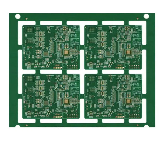
#Stackup Design
Explore tagged Tumblr posts
Visit Tumblr Blog
Explore Tumblr blogs with no restrictions, modern design and the best experience.
Last Seen Tumblr Blogs


Fun Fact
Post activity is at the highest at 4:00 pm EDT; notes peak at 10:00 pm EDT.
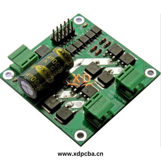
Text
Multilayer pcb is circuit boards composed of two or more conductive layers (copper layers). The copper layer is pressed together by the resin layer (prepreg).
King Credie manufacture multilayer pcb up to 32 Layer ,We accept pure single material or mixed-press materials ( e.g., FR4,Rogers,Polymide,metal Core).
#Multilayer PCB Stackup Design#Multilayer PCB Design#Multilayer Stackup Design#Multilayer Stackup#PCB Stackup Design#Stackup Design#PCB Design#Multilayer Design#Multilayer PCB Stackup#Multilayer construct Design
0 notes
Text
Tips for PCB Stackup Layout
With the continuous emergence of high-speed circuits, the complexity of PCB boards is also getting higher and higher. In order to avoid the interference of electrical factors, the signal plane and the power supply layer must be separated, so it involves the design of multilayer PCB, that is, the design of laminated structure.
1. Avoid Direct Connection of Two Signal Planes
In a multilayer PCB, it usually includes a signal plane (S), a power plane (P) plane and a ground plane (GND). How are the three arranged?
Power and ground planes are usually undivided solid planes that provide a good, low-impedance current return path for current from adjacent signal traces. Therefore, the signal plane is mostly adjacent to the power plane or the ground plane. Moreover, the power supply layer and ground plane use a large area of copper (so the power supply layer and ground plane are also called copper layer), and the large copper film can provide shielding for the signal plane, which is conducive to impedance control and improvement of signal quality.
In addition, should try to avoid two signal planes directly adjacent to each other. Crosstalk is easily introduced between adjacent signal planes, resulting in circuit failure. Adding a ground plane between the two signal planes can effectively avoid crosstalk.
2. Most Top and Bottom Planes are Signal Planes
The top and bottom planes of a multilayer PCB are usually used to place components and a small number of traces, so they are mostly signal planes. Generally, the top plane is the component, and the bottom plane (the second plane) of the component can be set as the ground plane, providing the device shielding layer and providing the reference plane for the top plane wiring.
In addition, note that these signal traces on the top and bottom planes cannot be too long to reduce direct radiation from the traces.
3.Reference Plane Preferred the Ground Plane
Both the power plane and the ground plane can be used as reference planes and have a certain shielding effect.
The difference between the two is that: the power supply layer has a high characteristic impedance, and there is a large potential difference with the reference level; while the ground plane is generally grounded and used as a reference point for the reference level, its shielding effect is much better than that of the power supply layer.
Therefore, when choosing a reference plane, the stratum is preferred.
4. The High-speed Signal Layer is Located in the Middle Plane of the Signal
The high-speed signal transmission layer in the circuit should be the signal intermediate plane and sandwiched between two copper layers. In this way, the copper film of the two copper layers can provide electromagnetic shielding for high-speed signal transmission, and at the same time, it can effectively limit the radiation of the high-speed signal between the two copper layers without causing external interference.
5.The Power Plane and the Ground Plane are Preferably Paired
The power supply layer and the ground plane appear in pairs, shortening the distance between the power supply and the ground plane can reduce the impedance of the power supply, which is beneficial to the stability of the power supply and reducing EMI. In particular, the main power supply should be as adjacent to its corresponding ground plane as possible. In the case of high speed, you can add extra ground planes to isolate the signal plane, but it is recommended not to add more power planes to isolate, because the power plane will bring more high-frequency noise interference.
6.Copper Layer Balance Design
The copper layer, that is, the power plane or the ground plane, is best arranged symmetrically, such as the second plane and the fifth layer of the 6-layer board, or the third layer and the fourth layer should be copper-plated together, which is considered to be flat and horizontal in the process. Structural requirements, as unbalanced copper layers may cause warpage as the PCB expands.
7.Multiple Power Planes away from High-speed Signal Planes
Multiple power supply layers should be kept away from high-speed digital signal wiring. Because the multi-power supply layer will be divided into several physical regions with different voltages, if the signal power is close to the multi-power supply layer, the signal current on the nearby signal layer will encounter an unsatisfactory return path, making the return path A gap appears.
8.Use Even-numbered layers
The classic PCB stack-up design is almost entirely even-numbered, not odd-numbered. Even-numbered layers of printed circuit boards have cost advantages, and even-numbered layers are more resistant to board warpage than odd-numbered layers.
9.Arrange Routing on Adjacent Layers
In order to complete complex wiring, the transition between layers of traces is inevitable. The two layers spanned by a signal path are called a "routing combination". The best routing combination design is to avoid return current flow from one reference plane to another reference plane, but rather to flow from one point (surface) of one reference plane to another point (surface).
Therefore, wiring combinations are preferably arranged on adjacent layers, because a path through multilayers is not clear for return currents. Although the ground bounce can be reduced by placing decoupling capacitors near the vias or reducing the thickness of the dielectric between the reference planes, it is not a good design.
10.The Routing Directions of Adjacent Signal Planes are Orthogonal
On the same signal plane, the direction of most wiring should be consistent, and it should be orthogonal to the wiring direction of adjacent signal planes. For example, the wiring direction of one signal plane may be set to the "Y-axis" direction, and the wiring direction of another adjacent signal plane may be set to the "X-axis" direction.
On the other hand, how to do impedance control is a headache for many users, but Hitech Circuits makes everything so easy. Hitech Circuits will automatically calculate the line width and line spacing corresponding to different impedance controls according to different stacks, so as to do impedance matching for the user, without the need to perform complex impedance calculations manually, saving effort and worry!
0 notes
Text
Top-Tier PCB Fabrication Services for Every Industry
High-performance printed circuit boards (PCBs) continue growing across every industry. From consumer electronics to aerospace, medical devices to automotive systems, the quality of a PCB can determine the performance, efficiency, and durability of an entire product. That's why top-tier PCB fabrication services are more critical than ever — and why choosing the right PCB fabrication company can make or break your success.
At the heart of every advanced electronic product lies a well-engineered PCB. As a trusted PCB manufacturing company, our mission is to deliver high-quality, precision-fabricated PCBs that meet the specific needs of your project, no matter how simple or complex.
Precision Engineering for Maximum Performance
Our PCB fabrication services are built on a foundation of engineering excellence. We use state-of-the-art technology and a highly skilled team to produce PCBs that meet tight tolerances and rigorous quality standards. Whether you're working with a standard double-sided design or a multilayer, high-density interconnect (HDI) board, we have the capability to deliver with precision.
Key fabrication capabilities include:
Single, Double, and Multilayer PCBs
HDI and Rigid-Flex Boards
High-Frequency & High-Speed PCBs
Heavy Copper & Metal Core PCBs
Lead-Free & RoHS Compliant Options
Through Hole PCB Assembly and Surface Mount Technology (SMT)
Each board is fabricated using high-grade materials and strict process control to ensure superior reliability and performance in real-world applications. Whether you need quick turn PCB assembly services for a prototype or a full-scale production run, we’re ready to meet your deadline.
Serving a Broad Spectrum of Industries
What sets us apart as a full-service PCB manufacturing company is our versatility. We support customers across a wide range of industries, offering specialized expertise in each vertical:
Consumer Electronics – Smartphones, wearables, and smart appliances require compact, high-speed PCBs with impeccable performance.
Automotive – From powertrain systems to in-car infotainment, automotive electronics rely on durable, high-temperature-resistant boards.
Medical Devices – Life-saving equipment like imaging systems and portable monitors demand extreme precision and zero-defect standards.
Industrial Automation – PCBs for control systems, robotics, and sensors must withstand harsh environments and continuous operation.
Telecommunications – Our fabrication processes support high-frequency RF boards essential to telecom infrastructure and 5G devices.
Aerospace & Defense – We offer military-grade fabrication for mission-critical electronics with strict adherence to industry standards.
No matter your application, our team works closely with you to understand your technical requirements and deliver boards that exceed expectations.
Customized PCB Fabrication Solutions
Every project is unique, and we believe in delivering tailored solutions that align with your product's performance, budget, and production timeline. As an experienced PCB fabrication company, we provide comprehensive design-to-delivery support to streamline your workflow.
Whether you're at the prototyping stage or preparing for full-scale production, we offer:
Quick-Turn Prototyping
Small to High-Volume Production
Custom Stackups & Impedance Control
Material Selection Guidance
DFM (Design for Manufacturability) Feedback
Quick Turn PCB Assembly Services to accelerate product development
Our design support team is available to review your Gerber files, assist with layout optimization, and ensure that your design is perfectly matched to our manufacturing capabilities.
Uncompromised Quality and Certification Standards
Quality is non-negotiable. All our fabrication processes are governed by international standards and robust quality management systems. We conduct multi-stage inspections and automated optical testing (AOI) at every critical phase of production.
Certifications and quality assurances include:
ISO 9001:2015 Certified
IPC Class 2 & Class 3 Compliant
UL Certification
RoHS and REACH Compliance
Full Traceability of Materials and Processes
Whether it's high-volume orders or through hole PCB assembly projects with complex layouts, our goal is to deliver zero-defect PCBs that perform flawlessly in their intended environment, every single time.
Fast Turnaround and On-Time Delivery
In fast-moving markets, time-to-market is everything. That’s why we offer quick turn PCB assembly services with guaranteed lead times, giving you the flexibility to meet tight project deadlines without compromising on quality.
Our streamlined workflow, in-house capabilities, and experienced logistics team ensure that your PCBs are delivered on time and ready for assembly — whether you're local or overseas.
Your Trusted PCB Fabrication Partner
Partnering with us means more than just placing an order — it means gaining a dedicated team invested in your product’s success. As a full-service PCB fabrication company, our focus on innovation, precision, and customer service has made us a trusted name in the electronics manufacturing industry for startups, engineers, and Fortune 500 companies alike.
We invite you to experience the difference of working with a fabrication house that puts your needs first.
Let’s Build the Future Together
Ready to get started? Whether you have a complex multilayer board, a custom design requiring through hole PCB assembly, or need quick turn PCB assembly services, our expert team is here to help you move from concept to reality — faster and better than ever before.
Contact us today for a free quote or design consultation, and discover how a trusted PCB manufacturing company can elevate your next project.
Let me know if you'd like this adapted into a landing page, brochure copy, or SEO-optimized blog!
0 notes
Text
Dive into the complexities of 10-layer PCB stack-up with this comprehensive guide. Viasion outlines key design principles, layer configurations, and considerations to ensure optimal performance, signal integrity, and reliability in multilayer board designs.
0 notes
Text
Exploring Rigid-Flexible Circuits: Advantages, Applications, and Design Considerations Rigid Flexible Circuits
Introduce the concept of rigid-flex circuits, highlighting their significance in modern electronics and their ability to combine the advantages of both rigid and flexible PCBs.Emphasize the importance of understanding the unique features and design considerations of rigid-flex circuits for various applications.
Section 1: What are Rigid-Flexible Circuits? Rigid Flexible CircuitsRigid Flexible Circuits
Define rigid-flex circuits as hybrid PCBs that incorporate both rigid and flexible substrates interconnected to form a single, integrated circuit.Explain the construction of rigid-flex circuits, including rigid sections for component mounting and flexible sections for bending and conforming to 3D shapes.
Section 2: Advantages of Rigid-Flexible Circuits: Rigid Flexible CircuitsRigid Flexible Circuits
Discuss the key advantages of using rigid-flex circuits over traditional rigid or flexible PCBs, such as:
Reduced assembly time and complexity by eliminating the need for connectors and interconnects.
Enhanced reliability and durability due to fewer solder joints and interconnection points.
Space savings and weight reduction in compact electronic devices, leading to improved design flexibility and performance.
Section 3: Applications of Rigid-Flexible Circuits: Rigid Flexible Circuits
Explore the diverse applications of rigid-flex circuits across various industries, including:
Wearable electronics (e.g., smartwatches, fitness trackers).
Medical devices and implantable electronics.
Aerospace and defense systems (e.g., avionics, unmanned aerial vehicles).
Automotive electronics (e.g., instrument clusters, infotainment systems).
Consumer electronics (e.g., smartphones, tablets, foldable displays).
Section 4: Design Considerations for Rigid-Flexible Circuits: Rigid Flexible Circuits
Provide guidelines and best practices for designing rigid-flex circuits, including:
Optimizing the layout and placement of rigid and flexible sections to minimize stress and strain during bending and flexing.
Selecting appropriate materials and stackup configurations to meet mechanical, thermal, and electrical performance requirements.
Considering factors such as bend radius, bend cycles, and dynamic flexing for long-term reliability and durability.
Section 5: Manufacturing Challenges and Solutions: Rigid Flexible Circuits
Discuss common manufacturing challenges associated with rigid-flex circuits, such as material compatibility, registration accuracy, and assembly processes.Offer solutions and strategies for overcoming these challenges, such as utilizing advanced manufacturing techniques, automation, and quality control measures.
Section 6: Future Trends and Developments: Rigid Flexible Circuits
Highlight emerging trends and developments in rigid-flex circuit technology, including:
Advancements in flexible substrate materials with improved mechanical properties and thermal stability.
Integration of additive manufacturing and 3D printing technologies for customized and complex rigid-flex designs.
Adoption of flexible hybrid electronics (FHE) concepts for seamless integration of sensors, actuators, and electronic components into flexible substrates.
Conclusion: Rigid Flexible Circuits
Summarize the key points discussed in the article about rigid-flex circuits and their importance in modern electronics.Encourage further exploration of rigid-flex circuit technology and collaboration with experienced PCB designers and manufacturers to leverage its benefits for innovative electronic products.
0 notes
Text
#stackup#multilayerpcb#dfm#impedance#pcbmanufacturing#pcbmaterial#prepreg#core#pcbdesigner#pcbdesign#electronicsengineering#usa#europe
0 notes
Text
Decoding PCBA Board Manufacture: A Roadmap to Efficient Production
PCBA (Printed Circuit Board Assembly) board manufacture stands as a pivotal stage in the journey from electronic concept to tangible product. This blog offers a detailed roadmap, guiding both novices and seasoned professionals through the multifaceted process of PCBA board manufacture.
The journey initiates with an elucidation of PCBA board components, ranging from basic resistors to intricate microprocessors. Understanding the role and compatibility of each component is paramount in crafting a functional and efficient board.
Subsequently, the blog navigates through the intricacies of PCB fabrication, encompassing design optimization, material selection, and fabrication techniques. Through insights into surface finishes, layer stackups, and trace routing, readers will grasp the fundamentals necessary for creating robust and reliable PCBs.
The narrative then transitions to the assembly phase, shedding light on component placement, soldering methodologies, and quality assurance protocols. From manual soldering to automated pick-and-place systems, readers will gain insight into the diverse assembly techniques and their respective advantages.
Moreover, the blog addresses the significance of thorough testing and inspection procedures to identify and rectify potential defects before the final product reaches the market. Topics such as in-circuit testing, functional testing, and quality control standards underscore the importance of delivering reliable and high-performance PCBAs.
In conclusion, "Decoding PCBA Board Manufacture" serves as a comprehensive guide for navigating the complexities of PCB assembly manufacturing. By leveraging the insights and best practices shared in this blog, electronics enthusiasts and industry professionals alike can streamline their manufacturing processes, ultimately fostering innovation and excellence in the realm of electronic design and production.
#pcb circuit#fr4 pcb#pcb factory#circuit board#led circuit board#flex pcb#pcb assembly#aluminum pcb#fpc#ems pcba
0 notes
Text
.
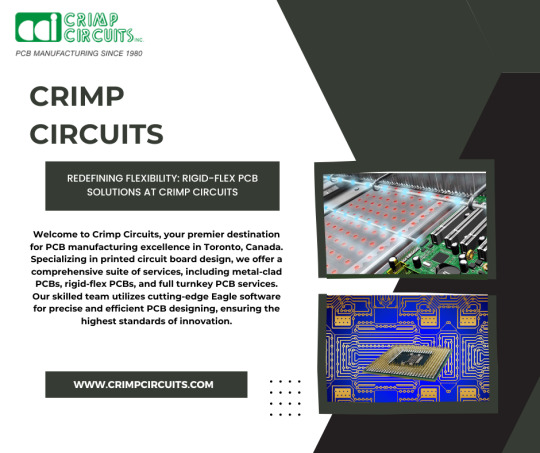
Rigid-Flex PCB: Revolutionizing Electronics with Flexibility and Rigidity
In the ever-evolving landscape of electronics, innovation often comes in the form of new materials and designs that push the boundaries of what is possible. Rigid-Flex PCB (Printed Circuit Board) is a prime example of such innovation, seamlessly combining the benefits of rigidity and flexibility to meet the demands of modern electronic devices. This hybrid construction has transformed the way electronic components are integrated, offering designers greater flexibility and versatility.
Understanding Rigid-Flex PCB: At its core, a Rigid-Flex PCB is a combination of rigid and flexible circuitry within a single board. It consists of both rigid sections, typically made of FR-4 material, and flexible sections, composed of polyimide or similar flexible substrates. This unique construction allows the board to bend or fold without compromising the integrity of the circuitry.
Versatility in Design: One of the primary advantages of Rigid-Flex PCB is its versatility in design. Traditional rigid boards are limited by their fixed shape, whereas flexible circuits can conform to non-planar surfaces. Rigid-Flex PCBs bridge this gap, offering designers the freedom to create 3D configurations that were once challenging or impossible with separate rigid and flexible boards.
Space Efficiency and Weight Reduction: The integration of rigid and flexible sections in a single board leads to enhanced space efficiency. Instead of using connectors and cables to link separate rigid and flexible boards, Rigid-Flex PCBs eliminate these additional components, reducing the overall size and weight of the electronic device. This is particularly beneficial in applications where size and weight constraints are critical factors.
Reliability and Durability: Rigid-Flex PCBs offer improved reliability compared to assemblies using connectors and cables. The elimination of interconnects reduces the points of failure, minimizing the risk of signal degradation, electrical noise, and mechanical wear. The seamless integration of rigid and flexible sections ensures durability, making Rigid-Flex PCBs suitable for applications subjected to repeated bending or flexing.
Complex Circuitry Integration: The combination of rigid and flexible sections facilitates the integration of complex circuitry within a compact space. Designers can strategically place rigid areas for components requiring stability and flexibility in sections that demand adaptability. This capability is especially advantageous in densely populated electronic devices where space optimization is critical.
Applications in Various Industries: Rigid-Flex PCB technology has found applications in a diverse range of industries. From aerospace and automotive to medical devices and consumer electronics, the adaptability of Rigid-Flex PCBs makes them suitable for numerous applications. In the automotive sector, for instance, Rigid-Flex PCBs are employed in airbag systems, control modules, and instrument clusters, benefiting from the space-saving and reliability features.
Challenges and Considerations: While Rigid-Flex PCBs offer significant advantages, their design and manufacturing present unique challenges. Designers must carefully consider factors such as material compatibility, bend radius, and layer stackup. Collaboration between electrical and mechanical engineers is crucial to ensure that the final design meets both electrical and mechanical requirements.
Conclusion: In conclusion, Rigid-Flex PCB technology represents a paradigm shift in the world of electronic design and manufacturing. Its ability to seamlessly blend rigidity and flexibility opens up new possibilities for compact, lightweight, and reliable electronic devices. As technology continues to advance, Rigid-Flex PCBs will likely play an increasingly pivotal role in shaping the future of electronic innovations, offering a harmonious blend of form and function in the realm of printed circuit boards.
For more details visit our website : www.crimpcircuits.com
#pcb manufacturing toronto#printed circuit board design#metal clad pcb#printed circuits#rigid flex pcb#full turnkey pcb services#turnkey pcb services#pcb parts#eagle software#pcb designing#flexible pcb#pcb assembly#printed circuit board manufacturers#pcb manufacturers in canada#circuit board manufacturers in canada#pcb quote#pcb prototype services in canada
0 notes
Text
Advancements in HDI PCB Technology: A Leap Towards Smaller, Faster, and More Efficient Electronics
In the ever-evolving world of electronics, the demand for smaller, faster, and more efficient devices has never been higher. High-Density Interconnect (HDI) Printed Circuit Boards (PCBs) have emerged as a game-changer in meeting these demands. HDI PCBs represent a technological leap that enables the development of sleeker, more powerful, and feature-rich electronic gadgets. This article explores the world of HDI PCBs, delving into their significance, manufacturing process, applications, and the impact they have on the electronics industry.
HDI PCBs: A Brief Overview
HDI PCBs are a specialized type of printed circuit board designed to optimize space usage and increase functionality. Unlike conventional PCBs, HDI PCBs offer a higher circuit density with multiple layers of closely packed components and traces. These boards are constructed using advanced manufacturing techniques, allowing for the creation of compact designs without compromising on performance.
The Manufacturing Process:
Creating HDI PCBs is a complex process that involves several stages. Here’s a simplified overview of the manufacturing process:
Layer Stackup: HDI PCBs consist of multiple layers, including inner layers, outer layers, and vias (connections between layers). The stackup is carefully designed to accommodate the required circuitry and components.
Laser Drilling: Laser drilling is a key step in HDI PCB manufacturing. It involves using laser technology to create small-diameter holes (microvias) that connect different layers of the board. This process allows for high-density component placement.
Copper Plating: After drilling, the microvias are plated with copper to establish electrical connections between layers. This process ensures reliable signal transmission and power distribution.
Surface Finishing: HDI PCBs are typically finished with various surface treatments, such as gold plating or solder mask, to protect the copper traces and improve solderability.
Component Placement: SMT (Surface Mount Technology) is used to mount electronic components onto the PCB. Advanced pick-and-place machines precisely position tiny components, ensuring optimal space utilization.
Applications of HDI PCBs:
HDI PCBs have found their way into a wide range of applications across industries. Some notable applications include:
Consumer Electronics: HDI PCBs are a cornerstone of smartphones, tablets, laptops, and wearable devices, enabling the compact design of high-performance gadgets.
Medical Devices: Medical equipment, such as pacemakers, MRI machines, and diagnostic devices, rely on HDI PCBs for their compactness and reliability.
Aerospace and Defense: HDI PCBs are crucial in aerospace applications, where size and weight constraints are significant factors.
Automotive Electronics: The automotive industry uses HDI PCBs in advanced driver-assistance systems, infotainment systems, and engine control units.
Industrial Automation: High-density PCBs are integral to the automation and control systems that drive modern factories and production lines.
Impact on the Electronics Industry:
HDI PCB technology has had a profound impact on the electronics industry in several ways:
Miniaturization: HDI PCBs have enabled the development of smaller and sleeker devices, leading to innovations like foldable smartphones and ultra-thin laptops.
Enhanced Performance: The high circuit density and optimized design of HDI PCBs result in improved signal integrity, reduced electromagnetic interference, and overall better performance.
Cost-Efficiency: Despite their complexity, advancements in HDI PCB manufacturing have made these boards more cost-effective over time, making them accessible to a wider range of applications.
Increased Functionality: HDI PCBs have opened the door to increased functionality in electronics, allowing for more features and capabilities in the same form factor.
Conclusion:
High-Density Interconnect (HDI) Printed Circuit Boards are a remarkable technological advancement that has revolutionized the electronics industry. Their ability to pack more functionality into smaller spaces has driven innovation across various sectors, from consumer electronics to aerospace and healthcare. As we continue to demand smaller, faster, and more efficient devices, HDI PCBs will remain at the forefront of this transformation, propelling us into a future filled with increasingly compact and powerful electronics
0 notes
Photo

Next extra seats.? These light weight chairs may be a good choice. Stack up if you don't use them. . #lightweight #lightchair #stackup #colorchairs #chairs . #chairdesigns #chair #seats #extraseats #seatingarea . #fantasticfurniture #furnituredesign #furniture #newchairs #newfurniture . . #renovation. #Design. #renovating #reno #renovatingSydney . #renovationconsultant #kingsmanconsultants @kingsmanconsultants #旅行好きな人と繋がりたい (at Sydney, Australia) https://www.instagram.com/p/B9Sb20YFcqj/?igshid=eea36sb5ol01
#lightweight#lightchair#stackup#colorchairs#chairs#chairdesigns#chair#seats#extraseats#seatingarea#fantasticfurniture#furnituredesign#furniture#newchairs#newfurniture#renovation#design#renovating#reno#renovatingsydney#renovationconsultant#kingsmanconsultants#旅行好きな人と繋がりたい
0 notes
Text
Thiết kế máy tính nhúng BeagleBone AM3359


Các hạng mục thiết kế mạch (PCB):
Placement và Routing chuyên nghiệp.
BOM list (danh sách linh kiện) với chi phí tối ưu nhất.
Thiết kết tuân thủ tiêu chuẩn: DFM (Design For Manufacturing) và DFA (Design for Assembly) đảm bảo SMT và sửa chữa dễ dàng.
Thiết kết tuân thủ EMI, EMC.
Thiết kết board nâng cao: Stackup design, Impedance control, Differential pair, RF...
https://epcb.vn/pages/thiet-ke-mach-thiet-bi-dien-tu-pcb-design-tai-tp-hcm
1 note
·
View note
Text
Exploring Rigid-Flexible Circuits: Advantages, Applications, and Design Considerations Rigid Flexible Circuits
Introduce the concept of rigid-flex circuits, highlighting their significance in modern electronics and their ability to combine the advantages of both rigid and flexible PCBs.Emphasize the importance of understanding the unique features and design considerations of rigid-flex circuits for various applications.
Section 1: What are Rigid-Flexible Circuits? Rigid Flexible CircuitsRigid Flexible Circuits
Define rigid-flex circuits as hybrid PCBs that incorporate both rigid and flexible substrates interconnected to form a single, integrated circuit.Explain the construction of rigid-flex circuits, including rigid sections for component mounting and flexible sections for bending and conforming to 3D shapes.
Section 2: Advantages of Rigid-Flexible Circuits: Rigid Flexible CircuitsRigid Flexible Circuits
Discuss the key advantages of using rigid-flex circuits over traditional rigid or flexible PCBs, such as:
Reduced assembly time and complexity by eliminating the need for connectors and interconnects.
Enhanced reliability and durability due to fewer solder joints and interconnection points.
Space savings and weight reduction in compact electronic devices, leading to improved design flexibility and performance.
Section 3: Applications of Rigid-Flexible Circuits: Rigid Flexible Circuits
Explore the diverse applications of rigid-flex circuits across various industries, including:
Wearable electronics (e.g., smartwatches, fitness trackers).
Medical devices and implantable electronics.
Aerospace and defense systems (e.g., avionics, unmanned aerial vehicles).
Automotive electronics (e.g., instrument clusters, infotainment systems).
Consumer electronics (e.g., smartphones, tablets, foldable displays).
Section 4: Design Considerations for Rigid-Flexible Circuits: Rigid Flexible Circuits
Provide guidelines and best practices for designing rigid-flex circuits, including:
Optimizing the layout and placement of rigid and flexible sections to minimize stress and strain during bending and flexing.
Selecting appropriate materials and stackup configurations to meet mechanical, thermal, and electrical performance requirements.
Considering factors such as bend radius, bend cycles, and dynamic flexing for long-term reliability and durability.
Section 5: Manufacturing Challenges and Solutions: Rigid Flexible Circuits
Discuss common manufacturing challenges associated with rigid-flex circuits, such as material compatibility, registration accuracy, and assembly processes.Offer solutions and strategies for overcoming these challenges, such as utilizing advanced manufacturing techniques, automation, and quality control measures.
Section 6: Future Trends and Developments: Rigid Flexible Circuits
Highlight emerging trends and developments in rigid-flex circuit technology, including:
Advancements in flexible substrate materials with improved mechanical properties and thermal stability.
Integration of additive manufacturing and 3D printing technologies for customized and complex rigid-flex designs.
Adoption of flexible hybrid electronics (FHE) concepts for seamless integration of sensors, actuators, and electronic components into flexible substrates.
Conclusion: Rigid Flexible Circuits
Summarize the key points discussed in the article about rigid-flex circuits and their importance in modern electronics.Encourage further exploration of rigid-flex circuit technology and collaboration with experienced PCB designers and manufacturers to leverage its benefits for innovative electronic products.
0 notes
Text
0 notes
Text
"Designing an Efficient PCB Circuit: A Comprehensive Guide for Electronics Enthusiasts"

In the dynamic world of electronics, creating a well-optimized Printed Circuit Board (PCB) circuit is a crucial skill for anyone venturing into hardware design. PCBs serve as the backbone of electronic devices, providing a compact and organized platform for connecting various components. This blog aims to demystify the process of designing a PCB circuit, offering valuable insights for both beginners and seasoned enthusiasts.
The journey begins with understanding the fundamentals of PCB design, including the selection of components, layout considerations, and the importance of signal integrity. The blog will delve into the role of schematic diagrams in visualizing the circuit, aiding in the identification of potential issues before the physical implementation.
Readers will gain insights into the significance of layer stackup and routing techniques to ensure optimal performance and minimize interference. The discussion will also touch upon the use of specialized software tools for PCB design, making the process more accessible and efficient.
Furthermore, the blog will address common challenges in PCB design and provide practical tips for troubleshooting and debugging. Real-world examples and case studies will be explored to illustrate successful PCB designs and the lessons learned from less-than-perfect implementations.
In conclusion, "Designing an Efficient PCB Circuit" aims to empower electronics enthusiasts with the knowledge and confidence to create well-crafted PCBs for their projects. Whether you're a hobbyist or a professional, mastering PCB design is a key step in unleashing the full potential of your electronic creations.
#pcb circuit#pcb factory#circuit board#flex pcb#led circuit board#pcb assembly#aluminum pcb#fr4 pcb#fpc
0 notes
Text
The Process of PCB Prototyping
In the technological era, PCBs play an important role. Printed Circuit Boards are foundation that enables the connection between electronic components and thus play an important role in multidisciplinary industries. As a critical component in the majority of industries, PCB design needs to be on the mark & meet demands of the hour; thus, design flaws must be avoided at all costs.
PCB designs are complex and require careful planning to achieve success in a single pass. There are numerous factors that influence the function of a PCB, and all of them can be tested before the PCB design is manufactured.
A prototype is an early sample of a design that is used to test the design and assist the manufacturer in streamlining the assembly process. Along with detecting flaws, prototyping serves the following purposes.
Assists in learning about circuit design in order to work according to requirements.
Assists in checking the functionality of PCB in a cost-effective manner.
To monitor PCB behavior under various environmental conditions such as temperature, pressure, and so on.
The PCB Prototyping Process begins with gathering all of the necessary information, such as the number of layers of PCB, board thickness, weight, and thickness of copper.
The first step is to learn about the system's electric parameters, which include voltages, signal types, circuit component type and location, as well as a detailed net wire listing and schematic.
Creating Schematics is a crucial step in determining the framework of a "nets connection". It refers to the design at the electrical level of the board’s purpose and function. To identify any errors in schematics, an ERC (Electric Rule Check) is performed.
Designing the PCB stackup
At this stage, the arrangement of copper and insulating layers are arranged to form a PCB. It aids in the design of high-density, high-performance PCBs with enhanced signal integrity, thermal management, and reliability.
Footprint Preparation
The preparation of the footprint is an important step in the PCB design process because it determines how the component will be physically mounted and connected to the circuit board.
Placing of Components
Component placement is an important step in the PCB design process. The placement of components has an impact on the circuit's functionality, reliability, and manufacturing. A few factors are considered most important when placing components, such as component orientation, signal flow, thermal considerations, mechanical constraints, and manufacturing requirements.
Routing the Traces
Once the components have been installed and the footprint has been completed, the board is ready to route the traces, which involves connecting the path segments.
Marking
Adding labels, identifiers, markings, or reference designators to the layout aids in determining whether or not specific components will be used on the board.
Generate Design
The process contains all of the information pertaining to the circuit board. The PCB is ready for fabrication once the design is completed.
PCB Fabrication
It is the process of making a PCB from a design file. PCB fabrication is a complex process that necessitates specialized equipment and expertise for surface finishing and cutting. Any flaws or errors in the fabrication process can lead to poor device or system performance or failure. To ensure the highest possible quality and dependability of the final product, it is critical to work with a reputable and experienced PCB fabrication service provider.
Assembly
The most important step in PCB prototyping is component assembly, which is followed by a final functionality test.
There are a few tricks that can help you complete the prototype process in one go, such as
Taking care of Spacing
Listing out all the components
Simply focusing on traces
While all of the above tricks are beneficial, there is one more factor that must be considered: preventing overheating throughout the process.
Hence, starting with a prototype makes the manufacturing process more cost-effective and efficient in the long run, resulting in higher quality and more predictable performance.
At PCB Power Market USA, we have no minimum order value, so you can carry out prototyping flawlessly. Think of us, when in need of PCB prototyping!
Original Source: https://www.pcbpower.us/blog/the-process-of-pcb-prototyping
0 notes
Text
Breakthrough Technologies: Exploring the Future of PCB Circuit Design
Printed circuit board (PCB) design is essential to the creation of cutting-edge electronic products in today’s continuously changing technological environment. Innovative PCB circuit design solutions are crucial as businesses and consumers want devices that are more complex and compact. This article examines the prospects for PCB circuit design and presents ground-breaking innovations that promise to transform the market.

Designing PCB Circuits: Its Importance
Recognising PCBs
The basis for electrical connections and the foundation for parts like resistors, capacitors, and integrated circuits, PCBs comprise the core of contemporary electronic gadgets. The functionality, dependability, and manufactureability of electronic devices are significantly influenced by the design and arrangement of these boards.
Demands of a Changing Industry
Electronic devices becoming smaller, more powerful, and feature-rich as technology develops. Due to this development, PCB designers are under more pressure to produce compact boards that can hold more components while ensuring ideal signal integrity and thermal management.
What a PCB Circuit Design Does
The process of designing a PCB circuit is laying out and connecting electronic components physically on a board. Electrical engineering, materials science, and manufacturing process knowledge are prerequisites. Effective PCB circuit design promotes reliable electronic device operation and transfer of signals while minimising electromagnetic interference.
PCB Circuit Design Development
From Traditional to Modern
PCB (Printed Circuit Board) Design has advanced significantly from its infancy. The placement of individual components on a board and their wiring together were traditionally done manually to construct PCBs. But technological developments have revolutionised this industry and improved its accuracy and efficiency.
CAD (Computer-Aided Design) introduction
In the field of PCB circuit design, the arrival of Computer-Aided Design (CAD) software has completely changed the game. Using CAD tools, engineers can digitally design, simulate, and test circuits, greatly decreasing the time and effort needed to create intricate PCB layouts.
Integration and Miniaturisation
The need for smaller and more potent electrical devices has increased dramatically as a result of the quick development of technology. Component integration and miniaturisation inside PCBs have resulted from this. Engineers can now fit an astonishing amount of components onto a single board thanks to creative design processes and advanced manufacturing procedures, leading to smaller and more effective electronic gadgets.
New techniques for designing PCB circuits
1. Smaller size and more dense interconnects
Miniaturisation is a major consideration in PCB circuit design due to the demand for smaller electronic devices. Higher component density and interconnection are now possible thanks to improvements in manufacturing techniques like microvia technology and multilayer stacking. These developments make it possible for designers to create small layouts without sacrificing performance.
2. Rigid-Flex and Flexible PCBs
Flexible and rigid-flex PCBs provide distinctive design options for a range of applications. They enable flexible form factors, which are especially advantageous in applications for wearable electronics, medical devices, and aerospace. Compared to conventional rigid boards, these PCB types offer greater design flexibility, higher durability, and lower weight.
3. Signal Integrity and High-Speed Design
Signal integrity is increasingly important when electronic devices operate at higher frequencies. Techniques for high-speed PCB design that reduce signal degradation problems including crosstalk, reflections, and electromagnetic interference include differential signalling, controlled impedance routing, and advanced layer stackups. These methods make it possible to transmit high-speed communications successfully while preserving data accuracy.
4. Advanced Substrates and Materials
The performance and dependability of PCBs are significantly influenced by the substrate and material selection. Innovative materials, like high-temperature substrates and sophisticated laminates, provide better thermal management, less signal loss, and enhanced mechanical strength. Additionally, flexible substrates and conductive inks based on nanotechnology are creating new opportunities for PCB designs of the future.
5. Additive manufacturing and 3D printing
A number of industries, including PCB circuit design, have been transformed by the introduction of 3D printing and additive manufacturing. Complex three-dimensional structures with intricate connections can be made because to this technology. Traditional PCB manufacturing is pushed to its limits by 3D printed PCBs, which offer quicker prototyping, more customization choices, and enhanced design freedom.
6. Integration of the Internet of Things
The PCB circuit design is evolving to enable linked devices as a result of the growth of the Internet of Things (IoT). PCBs must have wireless connectivity, sensors, and power management features in order to support IoT integration. To satisfy the expectations of this networked age, designers are creating IoT-focused PCBs with improved energy efficiency, data processing capabilities, and secure connection protocols.
7. Artificial intelligence and automation
Automation and artificial intelligence (AI) are becoming increasingly important in expediting the design and production processes as PCB circuit designs become more elaborate and complex. AI algorithms can reduce signal interference, improve circuit layouts, and find potential design defects, saving time and money. Automation tools, like CAD software and robotic assembly systems, are accelerating, improving, and lowering the cost of PCB production. The PCB sector is being revolutionised by automation and AI, which is launching us into a future with effective and knowledgeable design processes.
Conclusion
PCB circuit design will be replete with innovative new technologies that will push the limits of what is conceivable in the electronics industry. These innovations are poised to revolutionise the market, from miniaturisation and high-density interconnects to flexible and rigid-flex PCBs, high-speed design, innovative materials, 3D printing, and IoT integration. PCB circuit designers must embrace these technologies to provide creative solutions as businesses and customers continue to seek smaller, more potent, and connected gadgets. PCB circuit designers may ensure they maintain their competitiveness and produce cutting-edge electronics that influence the future by staying at the forefront of these innovations.
About the Author: Avi Gupta, Founder of PCB Must Innovations, is a dynamic force in the world of electronics design. With a wealth of industry experience, Avi thrives on solving intricate problems and delivering dependable solutions. A tech enthusiast, Avi stays ahead of trends while cherishing precious moments with family. Avi could be reached at [email protected]
Electronics, Electronics Design
0 notes