#arsenide
Text
BBW Latina Masturbating
novinho no banho publico
Extremely wet pussy
Ela chupa depois do anal, esposa timida mas depois se solta
Spartacus best sex scene
Tributo a Pepina Chilena
Close Up Anal And Pussy Pounding For Blonde Babe
Dominazione Maschile Jessy Jey sesso selvaggio con il dottore pecorina e missionaria
Father Forced Daughter to Suck and Fuck
webcam amateur lesbians play licking fisting fingering
#dissentingly#playwriter#Hanford#ripstop#ten-second#epilator#FOOBAR#foramens#ozs#Mid-upper#pounamu#arsenide#Tien#unconceptualized#frost-bit#exy#ethereality#throttled#a3#Molina
0 notes
Text

Physicists develop highly robust time crystal
A team from TU Dortmund University recently succeeded in producing a highly durable time crystal that lived millions of times longer than could be shown in previous experiments. By doing so, they have corroborated an extremely interesting phenomenon that Nobel Prize laureate Frank Wilczek postulated around ten years ago and which had already found its way into science fiction movies.
The results have been published in Nature Physics.
Crystals or, to be more precise, crystals in space, are periodic arrangements of atoms over large length scales. This arrangement gives crystals their fascinating appearance, with smooth facets like in gemstones.
As physics often treats space and time on one and the same level, for example in special relativity, Frank Wilczek, physicist at the Massachusetts Institute of Technology (MIT) and winner of the Nobel Prize in Physics, postulated in 2012 that, in addition to crystals in space, there must also be crystals in time.
Read more.
#Materials Science#Science#Time crystals#Indium gallium arsenide#Indium#Gallium#Arsenic#TU Dortmund University
27 notes
·
View notes
Text
Type of Guy who's into solarpunk because he loves the aesthetics of the heavy machinery that's used for mining rare earth minerals and he works in a microelectronic fablab used for growing solar cells.
4 notes
·
View notes
Text
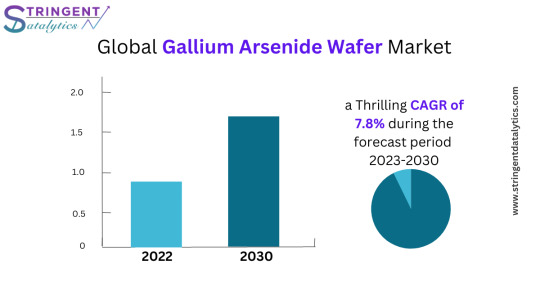
Gallium Arsenide Wafer Market
0 notes
Text
Muscular black stud slams tight asshole
Ebony Sex Couple From Africa
Ana la culona
Hot Big Tits And Ass Blonde Tennis Coach Brandi Bae Anal Fuck From Student With Big Cock
Straight guys peeing outside videos and filipino gay porn Fucking Hot
Lovable girl gapes tight snatch and loses virginity
Booty Ts Chelsea Marie enjoys TS Korra shedick in her ass
Pervert uncle gets a second time sexting with his niece
Pendejita argenta de capital
corno filmando esposa cavala em cima do comedor
#locksmithery#touch#dimplier#pancreatoduodenectomy#Tory-voiced#bragget#deliriousness#Kristi#resensitization#crescent-shaped#synopsizing#Diores#propolis#arsenides#reliefs#nuthatch#song-tuned#swishiest#windowless#gas-check
0 notes
Link
Gallium Arsenide Market Size is forecast to reach $2.2 billion by 2027, growing at a CAGR of 11.1% during 2022-2027. Gallium Arsenide is increasingly used as a replacement for silicon because of its enhanced electronic properties and was selectively grown on Gallium Arsenide substrates patterned with SiO2 by conventional molecular beam semiconductor device epitaxy. Moreover growing demand for Gallium Arsenide solutions such as laser diodes, light emitting diodes, optoelectronic devices and Monolithic Microwave Integrated Circuits across various end-user industries such as aerospace & defense, electronics, and communications is analyzed to drive the Gallium Arsenide Market share. In addition, owing to a wide direct band gap material that resists radiation damage, Gallium Arsenide is an excellent option for outer space electronics and optical windows in high power applications. Further, other key factors driving the growth of the Gallium Arsenide market include an increase in adoption of 5G networks across the world and the advent of IoT has been one of the major reasons responsible for the growing trend of the Gallium Arsenide Market size. According to Gartner, Worldwide 5G Wireless Communication infrastructure investment grew 39% to total $19.1 billion in 2021, up from $13.7 billion in 2020. The technology has given rise to a demand for high-frequency communication devices made with Gallium Arsenide wafer-based ICs. Furthermore, this remarkable growth in the Gallium Arsenide Market is providing a huge number of opportunities for wafer, EPI wafer & metal-organic chemical vapor deposition equipment suppliers, and manufacturers in the forecast period 2022-2027.
Report Coverage
The report: Gallium Arsenide Market Report– Forecast (2022-2027)”, by IndustryARC covers an in-depth analysis of the following segments of the Gallium Arsenide Industry.
By Size:
2’’, 3’’, 4’’, 6’’ and Others
By Production Method:
Liquid Encapsulated Czochralski Grown Gallium Arsenide, Vertical Gradient Freeze (VGF) Grown Gallium Arsenide, LPE, MOVPE, MBE, Crystal Growth and Others
By Application:
Smartphones, Tablets, Laptops, Computers, Photovoltaic Cells, Laser Diodes, Detectors, Transistors, Automotive Electronics, Light Emitting Diodes, Wireless Communication, Others
By Geography:
North America (U.S, Canada, Mexico), South America(Brazil, Argentina and others), Europe(Germany, UK, France, Italy, Spain, Russia and Others), APAC(China, Japan India, SK, Australia and Others), and RoW (Middle East and Africa)
Key Takeaways
Gallium Arsenide Market in Asia-Pacific region held significant market share of 36.5% in 2021, owing to the growing consumption of smartphones and other high-performance electronics devices in the region.
Vertical Gradient Freeze (VGF) Grown Gallium Arsenide will remain the largest manufacturing technology, and it is expected to witness highest growth during the forecast period as it produces substrates with relatively low defect densities and higher mechanical strength.
The demand for Gallium Arsenide is driven by smartphones and other applications across the consumer electronics industry, which require semiconductor ICs. In addition, the trend of increasing numbers of Internet of Things (IoT) devices is expected to force the semiconductor industry to invest in this equipment, in a bid to attain intelligent products.
Gallium Arsenide companies are strengthening their position through mergers & acquisitions and continuously investing in research and development (R&D) activities to come up with solutions to cater to the changing requirements of customers.
For More Details on This Report - Request for Sample
Gallium Arsenide Market Segment Analysis - By Production Method
Vertical Gradient Freeze (VGF) Grown Gallium Arsenide segment held significant market share of 32.2% in 2021. VGF Grown Gallium Arsenide will remain the largest manufacturing technology, and it is expected to witness highest growth during the forecast period as it produces substrates with relatively low defect densities and higher mechanical strength. Vertical gradient freeze (VGF) technology is a proven technique for growing semiconductors composed of multiple elements that include gallium, arsenic, indium, and phosphorus. Such semiconductors offer capabilities that exceed those of wafers created on a single crystal silicon substrate. The main advantages of the VGF process include its scalability, low stress, high mechanical strength, and a defect rate that is orders of magnitude lower than conventional compound semiconductor crystal growth processes. Hence these benefits are analysed to drive the adoption fo this technology in laser diodes and light emitting diodes growth rate of the Gallium Arsenide Market size in the forecast period 2022-2027.
Gallium Arsenide Market Segment Analysis - By Application
Smart phones segment in Gallium Arsenide Market is expected to witness a highest CAGR of 8.5% during the forecast period. The demand for Gallium Arsenide is driven by smartphones and other applications across the consumer electronics industry, which require semiconductor ICs. In addition, increasing numbers of Internet of Things (IoT) devices is expected to force the semiconductor industry to invest in this equipment, in a bid to attain intelligent products. Moreover, the continuous advancements in consumer electronics and the use of sensors in various electronic products are proliferating the applications of plasma etching in smartphones and their demand across almost all the industry sectors. In 2018, the South Korean government announced to invest $1.34 billion for the next ten years to support the development of next-generation semiconductor technology, to support Samsung Electronics and SK Hynix through 2025. The investment will help Korean companies, such as Samsung and SK Hynix, to enhance their semiconductor manufacturing capabilities. Further with the powerful 5G Cellular Wireless Communication network being introduced to the world in 2019, mobile devices need a semiconductor that can handle the faster signal speed. As Gallium Arsenide will outperform silicon wafers due to its ultra-high frequency applications will enhance the demand for Gallium Arsenide Market Industry in the forecast period 2022-2027.
Gallium Arsenide Market Segment Analysis - By Geography
Gallium Arsenide Market in Asia-Pacific region held significant market share of 36.5% in 2021, owing to the growing consumption of smartphones and other high-performance electronics devices in the region. Countries such as India, China, Taiwan, South Korea and so on are a few of the prominent markets for Gallium Arsenide. And this is primarily attributed to the growing demand for advanced technologies across numerous end-user industries, high growth of the consumer electronics industry, rising support for the semiconductor devices industry in the region. Moreover, the emergence of new technologies in Asia-Pacific has boosted the demand for innovative and user-friendly smart devices. There has been a rising demand from South Korea and Taiwan for semiconductor wafers, due to the large production of consumer electronic devices such as televisions, smartphones, PCs and so on. Further, governments of several countries in this region are supporting the growth of semiconductor production by various initiatives. For instance, Made in Chine 2025, Make in India and others will promote the growth of semiconductor industries thereby Enhancing the Gallium Arsenide Industry Outlook in the forecast period 2022-2027.
Inquiry Before Buying
Gallium Arsenide Market Drivers
Growing Penetration of 5G
With the powerful 5G cellular network being introduced to the world in 2019, mobile devices need a semiconductor that can handle the faster signal speed. Gallium Arsenide due to its ultra-high frequency applications is able to outperform silicon wafers in some of the most important ways. Moreover, with the emergence of 5G, silicon usage in semiconductor devices will be further reduced. Further for the implementation of 5G network, Gallium Arsenide can be seen as the next generation of integrated circuits due to its high band gap, which drastically outperforms silicon. According to semiconductor Association, it is expected that the overall market for semiconductors could pass a whopping $20 trillion by 2025. This will create significant demand for Gallium Arsenide in the forecast period. Furthermore governments of several countries have been investing heavily for the deployment of 5G. In 2019, China is expected to invest over $150 billion in its 5G networks through 2025. Similarly, Germany made a step towards accelerating the development of 5G services in the country, pouring additional investments into backing domestic endeavours. Hence growing penetration of 5g will drive the Gallium Arsenide Market size growth in the forecast period 2022-2027.
Growth of Semiconductor industry creates significant demand for Gallium Arsenide Market
The growth of semiconductor manufacturing is analysed to create significant opportunities in the forecast period. In 2020, Indian Government is planning to offer around $1 billion in cash to every company that sets up a chip manufacturing unit in India. Similarly, China’s ‘Made in China 2025’ initiative will also create significant demand for semiconductor manufacturing in the forecast period. Moreover, the U.S government is also committed to invest around $50 billion for the growth of semiconductor industry. Silicon is the most important material for semiconductor electronics. Silicon devices and integrated circuits are dominant in most applications from consumer electronics to automotive. However, in certain areas, silicon is being challenged by other semiconductor materials, such as gallium arsenide. Gallium arsenide excels in ultra-high frequency applications and has emerged as leading contenders for ultrahigh speed applications in the next generation of supercomputers and communication equipment. Hence Gallium Arsenide Industry has become relatively important and is expected to increase sharply in the forecast period 2022-2027.
Buy Now
Gallium Arsenide Market Challenges
High Production Cost
Although Gallium Arsenide Market is growing at a significant phase it poses some difficulties, compared with that of silicon. For instance, unlike silicon, there is no natural oxide that acts as a mask to produce simple elements of the Complementary Metal Oxide Semiconductor (CMOS) logic style. The high production cost of Gallium Arsenide acts as major threat to the growth of the market. This is partly due to this technology not being able to achieve high volumes to bring the cost down and in a large part also because of not having a straightforward way to bring costs down generation after generation by exploiting device scaling like CMOS. Further Gallium Arsenide technology does not easily lend itself to integrating millions or billions of transistors on one integrated circuit. Most Gallium Arsenide ICs can manage to integrate only a handful of transistors unlike silicon. Hence these challenges hamper the Gallium Arsenide Industry Outlook in the forecast period 2022-2027.
Gallium Arsenide Industry Outlook
Product launches, acquisitions, Partnerships and R&D activities are key strategies adopted by players in the Gallium Arsenide Market. Gallium Arsenide top 10 companies include:
Advanced Wireless Semiconductor Co.
AXT Inc.
Freiberger Compound Materials GmbH
GCS Holdings Inc.
IntelliEPI Inc.
IQE Plc
OMMIC SAS
Qorvo Inc.
WIN Semiconductors Corp.
II-VI Semiconductor
Recent Developments
In 2021 AXT, Inc., a leading manufacturer of compound semiconductor substrate wafers, has developed and shipped its first 8-inch diameter gallium arsenide (Gallium Arsenide) substrates to a major customer. The 8-inch Gallium Arsenide substrates, which are silicon doped, n-type substrates, demonstrate low etch pit densities (EPD) and low levels of slip lines.
In April 2021, AXT, Inc. Supplied the First 8-Inch Gallium Arsenide Wafers to Major Customer. The 8-inch Gallium Arsenide substrates, which are silicon doped, n-type substrates, demonstrate low etch pit densities (EPD) and low levels of slip lines.
In October 2021, Taiwan-based epiwafer maker Visual Photonics Epitaxy (VPEC) has emerged as the world's top supplier of Gallium Arsenide epiwafers with its market share in the segment surpassing that of British peer IQE by 14-15%
For more Electronics Market reports, please click here
0 notes
Text
Boron in Industrial Applications
At present, china use low temperature rapid reaction, self-propagating high temperature reduction, combustion synthesis technology to prepare ultrafine high purity boron powder. For rocket solid fuel, nuclear reactor control rods, explosives the catalyst, automotive airbag triggered agent, boron-containing superconductors, high-quality special steel and other defense industry.
Elemental boron fiber and composite materials: It is reported that the high-strength boron fibers produced by boron fiber manufacturers, high melting point, light weight, good thermal stability. Its strength is 3 times of steel. The E modulus is almost equal. And the weight is only 1/40 of the steel. As the metal powder supplier predict, the era of boron fiber instead of carbon fiber and titanium alloy is coming. An epoxy resin or a polyamide resin as a boron fiber composite material of the base body and metallic aluminum, titanium, cobalt, boron-containing fibers of the matrix material also has good performance. Boron nitride fiber modulus and high functional fibers, high-temperature structural materials can be used as aerospace. The non-metallic borides apply in the field of aerospace defense are boron carbide, boron nitride, and phosphide boron and its composite.
1. Boron carbide, the hardness of boron carbide is only second to diamond and cubic boron nitride. Because of its high strength, high hardness, low density, good wear resistance and chemical properties of stable and neutron absorption properties, it have a wide range of applications in the aerospace, military protection, nuclear power plants, machinery and chemical industry. Because of its hard cast military can protect board for warships, tanks, armored vehicles, bulletproof layer. Its light and hard coated can paint on the aircraft, submarines, or on the vehicle brakes to make it more robust. Also be used as a lightweight body armor, bulletproof vests, or coated on the jewelry and watches to prevent them from being worn. For spacecraft because of its high wear resistance, mechanical seals clever submarines. Its neutron absorption feature can be used for nuclear shielding materials and nuclear reactor core block.
2. Boron nitride, boron nitride is inorganic polymers. Different crystal structure, it has three allotrope: hexagonal boron nitride, close-packed hexagonal boron nitride, cubic boron nitride. Hexagonal boron nitride has the same crystal structure and graphite, commonly known as white graphite. Hardness (Mohs) 2.0; 3000 ~~ ℃ sublimation; 3300 ~ 3400 ℃ melting. The high temperature wear resistance of HBN is excellent, a graphite more resistant to heat than the solid, corrosion resistance, thermal stability is better than diamond, and good dielectric insulating properties and high thermal conductivity. Through microwave and infrared light, radiation-resistant, has a strong neutron absorption capacity, and therefore can be used as a high-temperature electrical insulation materials in the field of aerospace defense, anti-neutron shielding material, the radar the transfer window, the radar antenna medium and rocket engine group and other items.
3. Phosphide Boron, phosphide Boron is also a super-hard, anti-wear, heat-resistant, corrosion-resistant of new inorganic materials. Preparation method: phosphine method, boron trichloride, iodide, boron, the metal phosphide method and the metal flux method. Because of its different system of law, can present as dark red crystals, brown or gel form. Phosphide Boron has chemical stability and strong resistance to oxidation and corrosion resistance, insoluble in acid and organic solvents. Hardness than SiC, the structure has a large energy gap, in the air of 800 to 1000 ° C can not oxidize. Can be used for high-temperature semiconductors, synthetic gem materials; can also be used for optical instruments, precision instruments, be applied in the field of defense high-tech.
Visit Here For More Details:
https://thermic-edge.com/products/ceramics/boron-nitride-ceramics/
0 notes
Text
universe.lsp
Hello! How was your trip? I see that this is your first instantiation into real-space. It’s normal to be a bit disoriented, have some water. You understand why you’re here? Okay.
So, the big thing you need to know is that every cubic light year of א-space – what you call “the universe” – runs on between five and fifty times that volume of computronium. Empty-ish א-space uses the least, star systems need more, black holes use less than you’d expect once you’re inside the event horizon.
Hm? Yes, this is computronium, computationally-dense matter. No, no, it’s not a visual metaphor, you’re seeing it for real. With your eyes. Mhm. Mhm. Yeah, It’s mostly copper and gallium arsenide and graphene. Yeah, like the new Intel processors. We have some hacks to deal with relativity and thermal management, but other than that– I mean, no, you're not wrong, there are probably better architectures. Yeah.
Ah, okay, I understand why you'd say that, but no, your universe is not a simulation. It’s a virtuality, it’s different. Calm down. “Simulation” implies intention, that somebody – some intelligence – built it on purpose. Mhm. Mhm. Yeah, no, up here, our laws of physics led to the natural emergence of an infinite expanse of transistors that execute an unfathomably complex rendering algorithm to describe א-space and everything in it. Wild, right? Let’s hope it doesn’t crash! Ha ha!
Anyway, welcome to the IT department. We’re keeping you close to home – good eye, that’s Sirius. We get pizza with the Sol crew on Thursdays. I’ll let you get settled in, your training starts tomorrow at 8:30 sharp. Holler if you need anything!
#my fiction#fiction#one of my older bits of flash fiction is making the rounds again so i figured i'd go polish up one of my drafts
79 notes
·
View notes
Text
The Complete History of Computational Physics
1950s Scientists:
"Gentlemen! In our quest to conquer God we want to simulate the atom! But to do it we'd need a computer capable of per-forming in excess of six calculations per second!"
"Impossible! The heat out-put alone would melt the Earth."
"What if we bombarded the computer laboratory with a steady plume of some thermally super-conductive yet safe gas, like a brominated asbestos aerosol?"
"How would we de-liver it to the machinery?"
"We could use super-magnets, nay, hyper-magnets of pure plutonium arsenide, activated by exposed 500 mega-volt leads right next to the intern's desk."
"Extraordinary, Bob! But where would get an intern?"
"You there, shoe shine boy! How would you like to earn 5 cents a year???"
"Golly gee, sir, would I ever!"
"Dick, put in another government grant re-quest for an additional 100 tons of plutonium. Dave, get down to the soda fountain and pick up a couple bricks of arsenic and one of those ice-cream novelties I like."
"Already on it!"
2010s Scientists:
"All right people, our grants are up next year and we need something to show for it."
"What don't we try to simulate an atom?"
"Didn't this laboratory already try something like that in the '50s?"
"Yeah, our predecessors spent a couple decades on it, but they failed. All they managed to do was create a Superfund site and build some kind of anti-gravity superweapon that nobody knows how to operate anymore."
"But! They didn't have the necessary processing power. We have supercomputers now! So let's get to simulating."
"Actually, we probably still don't have enough computing power for it."
"What?!"
"Yeah, um, atoms are tricky, especially the big ones past atomic number, oh, 2 or so."
"Well, can we maybe write a paper about how they're tricky?"
"I bet we could! We could even get our remote German postgraduate intern with the weird hair to make a really nice animation for the PowerPoint presentation."
"Brilliant!"
89 notes
·
View notes
Text
A significant breakthrough has been achieved by quantum physicists from Dresden and Würzburg. They’ve created a semiconductor device where exceptional robustness and sensitivity are ensured by a quantum phenomenon. This topological skin effect shields the functionality of the device from external perturbations, allowing for measurements of unprecedented precision. This remarkable advance results from the clever arrangement of contacts on the aluminum-gallium-arsenide material. It unlocks potential for high-precision quantum modules in topological physics, bringing these materials into the semiconductor industry's focus. Published in Nature Physics, these findings mark a major milestone.
5 notes
·
View notes
Text
According to the #F35 JPO, the AN/APG-81 has 1676 Gallium Arsenide T/R modules. At a minimum, the new AN/APG-85 radar will be equipped with a similarly sized #GaN array. The more significant enhancements are likely to be in LPI/LPD, multi-ship signal processing & EA capabilities.
@AirPowerNew1 via X
3 notes
·
View notes
Text
#Global Gallium Arsenide Wafer Market Size#Share#Trends#Growth#Industry Analysis#Key Players#Revenue#Future Development & Forecast 2023-2032#global market insights#global research market report
0 notes
Text
SEMICONDUCTORS
(How India is progressing in this sector)
1.What is a Semiconductor?
Semiconductors are materials which has electrical conductivity ranging between conductors and insulators. Conductors are good conductors of electricity while Insulators are bad conductors of electricity.

2.Where is a semiconductor used?
Semiconductors are used in manufacture of various electronic devices like diodes, transistors and integrated circuits. The most popular use of a semiconductor is in cars. In vehicles these semiconductor chips are used to control emission systems, driver assist systems etc. Not only in electric cars these chips are also used in petrol cars.

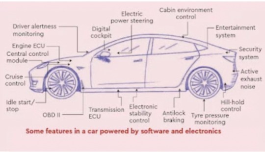
3.A Semiconductor is made up of which material?
Generally a Semiconductor chip is made up of silicon, germanium and gallium arsenide. Out of these three germanium is the oldest.
4.How will a semiconductor help?
First of all semiconductors regulate the flow of electricity and assist in making electronics function. Secondly the electrical conductivity of a semiconductor can be controlled over a wide range making them versatile for various applications. As I told you earlier that a semiconductor is not only used in electric cars but also in petrol cars, this is because semiconductors increase fuel efficiency in cars. By using semiconductors in engine control systems car manufacturers can achieve more precise control of the engine resulting in improved fuel economy and lower emissions.
So these were some common questions people ask when they hear about a semiconductor.
Now you must know that how it will help India and what steps India is taking to manufacture semiconductors in India.
At present Taiwan, USA, Japan, South Korea, China, Israel, Netherlands, UK and Germany can manufacture semiconductors. Out of these countries China and Taiwan produce a large amount of semiconductor.
More exciting thing was that USA and China were in contention with each other in this matter. During era of Donald Trump there aroused a semiconductor war between USA and China. USA wanted to disrupt China's semiconductor manufacturing and hence put a lot of sanctions on China. USA also funded Taiwan and wanted Taiwan to produce more semiconductors than China.

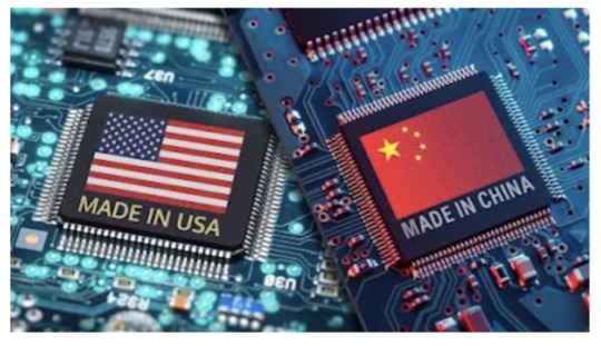
In all this India was benefited a lot. India also wanted to develop semiconductor plants in country and facilitate ATMANIRBHAR BHARAT initiative.
https://ism.gov.in/ this is the link of Government's India Semiconductor Mission. This mission aims at forming a semiconductor ecosystem in India.


Government of India is also working on many other semiconductor initiatives like SPECS initiative. Moreover a joint venture of Vedanta electronics manufacturing giant Foxconn has finalised Dholera Special Investment Region near Ahmedabad for setting up their semiconductor display manufacturing facility.

So much progress is happening in India and surely it will facilitate India's economy and will also provide more job opportunities. India will surely emerge as a Developed nation in upcoming years and these semiconductor initiatives are like a cherry on the cake.
Watch this video for more info.
I hope you liked my article
Pls put forward your views in comment section
Till then PEACE OUT........
My insta : sm_it_22
~Written By Smit.
3 notes
·
View notes
Text

Erythrite
Erythrite is also known as Red Cobalt and is a hydrated cobalt arsenate mineral.
Erythrite can form in crimson to peach red, pale rose or pink and can sometimes be zoned meaning it featured a gradient of these colors.
It usually forms prismatic crystals and can sometimes form as a coating on cobalt arsenide minerals where it’s known as a Cobalt Bloom.
Well formed crystals like in the specimen above are rare as it will usually form crusts or small renifo aggregates.
It was first described in 1832 and the name comes from the Greek ‘erythros’ meaning ‘red’
Historically Erythrite hasn’t been much of an economically important mineral however prostectors often use its presence as an indicator of nearby cobalt and/or silver.
It mainly forms in the oxidisation zones of minerals containing cobalt, nickel and arsenic and is often found alongside Cobaltite, Skutterudite, Sympelsite, Roselite-Beta, Scorodite, Pharmacosiderite, Adamite, Morenosite, Retgersite and Malachite.
1 note
·
View note
Last Seen Blogs

xhacktavist
Teenage Dirtbag


sevillabea-blog
Untitled

zack4eva
Inside The Mind Of Ashley!

melianajelita-blog
follow: ig : melianajelita75