#copper beryllium foil
Text
Beryllium Copper Strip Suppliers | Copper Strip | Copper Beryllium Foil
Looking for reliable Beryllium Copper Strip Suppliers? Look no further! Our website offers a wide range of Copper Strip options, including Copper Beryllium Foil. We provide high-quality products that are durable and efficient for various industrial applications. Explore our website to learn more about our Copper Strip selection and find the perfect fit for your project needs.
#copper strip#beryllium copper strip#beryllium copper strip suppliers#beryllium copper coil#copper beryllium foil#steel strips#copper strip price
0 notes
Text
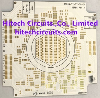
What is Ceramic PCB?
Ceramic PCB board is also called ceramic substrate, ceramic circuit board, ceramic copper coated plate, ceramic substrate refers to the copper foil directly bonded to alumina (Al2O3) or aluminum nitride (AlN) ceramic substrate or other ceramic substrate surface (single or double) on the special process board.
The ceramic pcb can be described as an organic binder and ceramic powder that conducts heat. The thermal conductivity at which this PCB is prepared is between 9 to 20W/m.
To explain further, ceramic PCBs are printed circuit boards, with ceramic as its base material. This base material is highly thermally conductive like aluminum nitride, alumina, and beryllium oxide. These are very effective in the transfer of heat from hot spots and then dissipating this heat over the entire surface.
Asides from this, the fabrication of ceramic PCB is done with the LAM technology. This technology is a laser quick activation metallization type. Therefore, ceramic PCBs are highly versatile and can easily substitute the whole traditional PCBs. This PCB will achieve this with even more enhanced performance and involving less complicated construction.
1. The difference between ceramic substrate and pcb board
Ceramic substrate is that we say ceramic circuit board, ceramic pcb and printed circuit board have the same circuit interconnection, through hole conduction characteristics. So what are the differences between ceramic substrate and pcb board?
(1)The thermal conductivity of PCB board and ceramic substrate is different
Ceramic substrate is made of ceramic substrate, that is, the medium is ceramic material, including alumina ceramic base, aluminum nitride ceramic base, silicon nitride ceramic base, ceramic heat dissipation performance is very good, the thermal conductivity of ceramic substrate from 25w to 230w, different ceramic medium thermal conductivity is different. The thermal conductivity of alumina ceramic substrate is 25w~30w, the thermal conductivity of aluminum nitride ceramic substrate is above 170w, and the thermal conductivity of silicon nitride ceramic substrate is 80w~90w. Then pcb board is usually the use of medium is fr4 or metal substrate, thermal conductivity is less than 3w, and the gap is too large compared with ceramic substrate, especially the need for high heat dissipation performance of the product field, ceramic substrate has become a very popular medium material.
2. Ceramic substrate and pcb board insulation is different
Ceramic substrate is generally line layer - ceramic base - line layer structure, ceramic substrate insulation is very good, is also determined by the ceramic material itself, no need to add insulation layer. pcb board needs to add an insulating layer to play a mobile insulation role, but the insulation effect is far less than ceramic substrate.
(3)The heat dissipation structure of ceramic substrate is different from that of pcb board
The heat dissipation structure of the ceramic substrate is the structure of the circuit layer - ceramic base - circuit board layer. Because there is no insulating layer in the middle, the heat of the device is transferred directly from the ceramic base to the circuit layer and the heat dissipation is out, the heat dissipation is fast and the effect is good. pcb board is the need for heat from the medium layer - insulation layer - line layer, separated by an insulation layer at the same time, the dielectric layer itself of the thermal conductivity is poor, then add heat conduction adhesive, heat conduction effect is still not improved, often can not achieve the purpose of rapid heat dissipation device. In particular, some high-power devices need to use ceramic substrate as a cooling substrate in the product field where the heat dissipation and temperature change is relatively large.
(4)Ceramic substrate and pcb board application is different
Ceramic substrate and pcb board application is different, mainly the performance of the two is different, ceramic substrate is used in high thermal conductivity, high heat dissipation, high insulation, product field, such as high power LED lighting, high power module, high-frequency communication, track power supply; Ordinary pcb board is used in some more extensive, heat dissipation, insulation and other requirements are not strict, used in private commercial commodities.
(5) The price of ceramic substrate is different from that of pcb board
The material and performance of ceramic substrate and pcb board are different, and the final decision is that their prices are different. The board of ceramic substrate is very high and the production cost is high.
Ceramic substrate has outstanding advantages, but the ceramic substrate is fragile and has a high scrap rate, which requires a high level of production technology. However, you can't make a circuit board with the size of more than one meter like ordinary pcb boards. Hitech Circuits has more than 10 years of experience in the ceramic circuit board industry, and many universities and R & D institutions are in cooperation, welcome to inquiry.
2.Ceramic substrate and high-frequency plate difference
The material is different. The ceramic substrate is made of aluminum oxide or aluminum nitride, and the high frequency plate is made of Rogers, Yaron, PTFE, etc., with low dielectric constant and high frequency communication speed.
Performance is different. Ceramic substrate is widely used in refrigeration and systems, high power modules, automotive electronics and other fields. High frequency board is mainly used in high frequency communication field, aviation, high-end consumer electronics and so on. High-frequency communication field involves heat dissipation requirements, usually need to be combined with the ceramic base and high frequency plate, such as high frequency ceramic pcb.
1. Application of ceramic substrate
Ceramic substrates are used in led chips to achieve better thermal conductivity. In addition, ceramic substrate is also used to make ceramic chips in the following electronic devices:
◆High power semiconductor module
◆Semiconductor cooler, electronic heater; Power control circuit, power mixing circuit
◆Intelligent power module; High frequency switching power supply, solid state relay
◆Automotive electronics, aerospace and military electronics components
◆Solar panel module; Telecommunications private exchange, receiving system; Laser and other industrial electronics
Application of ceramic substrate in third generation semiconductor
The mainstream power devices represented by MOSFET, IGBT and transistor occupy a place in their own frequency and power supply segments. Due to the comprehensive excellent performance of IGBT, it has replaced GTR, become the inverter, UPS, frequency converter, motor drive, high-power switching power supply, especially now the hot electric vehicle, high-speed rail and other power electronic devices in the mainstream devices.
Application of alumina ceramic substrate in electronic power field
In the field of power electronics, such as power switching power supply, electric drive, etc., dielectric ceramic substrate is needed to achieve better thermal conductivity, prevent current burn out and short circuit.
Application of alumina ceramic co-fired plate in lithium battery industry
With the recommendation of artificial intelligence and environmental protection, the automobile industry has also launched electric cars, mainly through battery storage. Lithium batteries made of ceramic substrate can achieve better current and heat dissipation functions, promoting the market demand for new energy vehicles.
2. Advantages of ceramic substrate
A. The thermal expansion coefficient of ceramic substrate is close to that of silicon chip, which can save Mo sheet of transition layer, save labor, save material and reduce cost;
B. Reduce the welding layer, reduce the thermal resistance, reduce the cavity;
C. Under the same load flow, the wire width of copper foil 0.3mm thick is only 10% of that of ordinary printed circuit board;
D. Excellent thermal conductivity, so that the chip packaging is very compact, so that the power density is greatly increased, improve the reliability of the system and device;
E. Ultra-thin (0.25mm) ceramic substrate can replace BeO, without environmental toxicity problems;
F. Large load capacity, 100A current continuously through 1mm wide 0.3mm thick copper body, temperature rise about 17℃; With 100A current continuously passing through a 2mm wide 0.3mm thick copper body, the temperature rise is only about 5℃.
G. Low thermal resistance, 10×10mm ceramic substrate 'thermal resistance of 0.63mm thickness of ceramic substrate is 0.31K/W, 0.38mm thickness of ceramic substrate is 0.19K/W, 0.25mm thickness of ceramic substrate is 0.14K/W.
H. High insulation and high pressure resistance to ensure personal safety and equipment protection.
I. New packaging and assembly methods can be realized, so that the product is highly integrated and the size is reduced.
3. Ceramic substrate technology
At present, the common types of ceramic heat dissipation substrate include HTCC, LTCC, DBC and DPC. DBC and DPC for the domestic in recent years to develop mature, and energy production of professional technology, DBC is the use of high temperature heating Al2O3 and Cu plate combination, its technical bottleneck is not easy to solve the problem of micro-pores between Al2O3 and Cu plate, which makes the mass production energy and yield of the product by the greater challenge. DPC technology is the use of direct copper plating technology, Cu deposition on the Al2O3 substrate, its process combined with the material and film technology, its product is the most commonly used ceramic cooling substrate in recent years. However, its material control and process technology integration ability requirements are high, which makes the technical threshold of entering the DPC industry and stable production is relatively high.
(1) HTCC (High-Temperature Co-fired Ceramic)
The manufacturing process of HTCC is very similar to that of LTCC. The main difference is that the ceramic powder of HTCC is not added with glass material. Therefore, the ceramic powder of HTCC must be dried and hardened into embryonic form at a high temperature of 1300~1600℃. Due to its high co-firing temperature, the choice of metal conductor materials is limited, its main materials for high melting point but poor conductivity tungsten, molybdenum, manganese... Such as metal, and finally laminated sintering molding.
(2) LTCC (Low-Temperature Co-fired Ceramic)
LTCC is also known as low-temperature co-fired multilayer ceramic substrate. In this technology, inorganic aluminum oxide powder and about 30%~50% glass material are combined with organic binder to make it evenly mixed into mud slurry. Then, the slurry is scraped into sheets with a scraper, and then through a drying process, the sheet slurry is formed into a thin piece of raw blank. As the transmission of signals at all levels
For the internal lines of LTCC, the screen printing technology is used to fill holes and print lines on the raw embryos, and the internal and external electrodes can be used respectively of silver, copper, gold and other metals. Finally, the layers are stacked and sintered in the sintering furnace at 850~900℃.
(3) Direct Bonded Copper (DBC)
Direct copper coating technology is the use of copper oxygen eutectic liquid directly on the ceramic coating, the basic principle is to introduce an appropriate amount of oxygen between copper and ceramic before or during the coating process, in the range of 1065℃~1083℃, copper and oxygen form Cu-O eutectic liquid, DBC technology uses the eutectic solution to chemically react with the ceramic substrate to form CuAlO2 or CuAl2O4 phase on the one hand, and to infiltrate the copper foil to realize the combination of the ceramic substrate and copper plate on the other hand.
(4) DPC (Direct Plate Copper)
DPC is also known as direct copper-plated substrate. Take DPC substrate process as an example: First of all, the ceramic substrate is pre-treated and cleaned, and the ceramic substrate is sputtered on the ceramic substrate and combined with the copper composite layer by using the vacuum coating technology of thin film manufacturing. Then the circuit is made by the re-exposure, development, etching and film removal process with the yellow light microshadow photoresistance. Finally, the thickness of the circuit is increased by electroplating/electroless plating deposition, and the metallized circuit is made after the photoresistance is removed.
3. Production process of ceramic substrate
1. Drilling
Ceramic substrate is generally used by laser punching, compared with the traditional punching technology, laser punching technology has the advantages of high precision, fast speed, high efficiency, large-scale mass punching, suitable for the vast majority of hard and soft materials, no loss to tools, in line with the printed circuit board high density interconnection, fine development.
Through the laser drilling process of ceramic substrate has high bonding force of ceramic and metal, no falling off, foaming phenomenon, to achieve the effect of growth together, high surface smoothness, roughness in 0.1μm ~ 0.3μm, laser drilling aperture in 0.15mm-0.5mm, even can reach 0.06mm.
2、Copper-clad
Copper coating refers to the area without wiring on the circuit board covered with copper foil, connected with the ground wire, in order to increase the ground wire area, reduce the loop area, reduce voltage drop, improve power efficiency and anti-interference ability. Copper coating can not only reduce the ground impedance, but also reduce the cross-sectional area of the loop and enhance the mirror loop of the signal. Therefore, the copper coating process plays a very key role in the ceramic substrate PCB process, incomplete, truncated mirror loop or incorrect position of the copper layer often lead to new interference, have a negative impact on the use of the board.
3. Etching
Ceramic substrates also need to be etched, with the circuit pattern pre-coated with a lead-tin resist layer, and then chemically etched away the unprotected, non-conductive copper to form the circuit. Etching is divided into inner layer etching and outer layer etching, inner layer etching using acid etching, with wet film or dry film as corrosion resistance; The outer etching is alkaline etching with tin and lead as resist.
There are many kinds of manufacturing process of ceramic products in circuit board factory. It is said that there are more than 30 kinds of manufacturing processes, such as dry pressing, grouting, extrusion, injection, casting and isostatic pressing. Because the electronic ceramic substrate is a "flat" type, the shape is not complicated, the manufacturing process of dry forming and processing is simple and the cost is low, so most of them use dry pressing forming method. The manufacturing process of dry press PCB electronic ceramics mainly includes blank forming, blank sintering and finishing, forming circuit on the substrate.
1. Green manufacturing of ceramic substrate (forming)
Use high purity alumina (content ≥95% Al2O3) powder (different particle sizes are required depending on the purpose and manufacturing method. For example, from a few illiterates to tens of microns) and additives (mainly adhesives, dispersants, etc.). Form a "paste" or processed material.
(1) Dry pressing of ceramic substrate to produce green parts (or "green").
Dry pressing billet is the use of high purity alumina (electronic ceramics with alumina content greater than 92%, most of the use of 99%) powder (dry pressing particles shall not exceed 60μm, for extrusion, rolling, injection and other powder particles should be controlled within 1μm) add the appropriate amount of plasticizer and binder, mixed evenly after dry pressing billet. At present, the offspring of square or round pieces can reach 0.50mm, or even ≤0.3mm (depending on plate size). Dry pressed billets can be processed before sintering, such as dimensioning and drilling. Machining, but be careful to compensate for the size shrinkage caused by sintering (magnify the size of the shrinkage).
(2) Production of green billet by ceramic substrate spreading method.
Flow glue liquid (aluminum oxide powder + solvent + dispersant + adhesive + plasticizer mixed evenly + screening) manufacturing + flow casting (in the flow casting machine glue on metal or heat-resistant polyester belt) + drying + trimming (can also be other processing) + degreasing + sintering and other processes. It can realize automation and scale production.
2. Sintering and finishing of green billet after sintering. The raw parts of ceramic substrate often need to be "sintered" and finished after sintering.
(1) Sintering of raw ceramic substrate.
Ceramic billet "sintering" refers to the process of "sintering", the billet (volume) in the cavity, air, impurities and organic matter such as dry pressure removal, so that its volatilization, combustion, extrusion, and removal of alumina particles. Achieve close contact or combined growth process, so after sintering of ceramic green billet, there will be weight loss, size shrinkage, shape deformation, compressive strength increase and porosity reduction and other changes.
The sintering methods of ceramic billet are as follows: ① atmospheric sintering, non-pressure sintering will bring large deformation; ② pressure (hot pressing) sintering, pressure sintering, can get good flat products is the most commonly used method; ③ Hot isostatic sintering is the use of high pressure hot gas sintering. Its characteristic products are finished at the same temperature and pressure. All kinds of performance balance, the cost is relatively high. In the added value of products, or aerospace, national defense and military products in the use of this sintering method, such as the military field of mirrors, nuclear fuel, barrel and other products. The sintering temperature of dry pressed alumina green billets is mostly between 1200℃ and 1600℃ (depending on composition and flux).
(2) Finishing of ceramic substrate after sintering (cooked) blank.
Most sintered ceramic billets require finishing. The purpose is: ① to obtain a flat surface. In the process of high temperature sintering of green billet, due to the imbalance of particle distribution, voids, impurities and organic matter in the green billet, it will cause deformation, unevenness or excessive roughness and difference. These defects can be solved by surface finishing; ② Obtain high finish surface, such as specular reflection, or improve lubricity (wear resistance).
Surface polishing treatment is to use polishing materials (such as silicon carbide, B4C) or diamond sand paste to gradually polish the surface from coarse to fine abrasive. Generally speaking, the use of AlO powder or diamond paste ≤1μm, or laser or ultrasonic processing to achieve.
(3) strong (steel) treatment.
After surface polishing, in order to improve the mechanical strength (such as bending strength, etc.), electronic ray vacuum coating, sputtering vacuum coating, chemical vapor evaporation and other methods can be used to plating a layer of silicon compound film, through 1200℃ ~ 1600℃ heat treatment, can significantly improve the mechanical strength of ceramic parts!
3. Form a conductive pattern (circuit) on the substrate
To process conductive graphics (circuits) on ceramic substrates, it is necessary to manufacture copper-coated ceramic substrates first, and then to manufacture ceramic printed circuit boards according to PCB technology.
(1) Forming a copper-covered ceramic substrate. There are currently two methods of forming copper-coated ceramic substrates.
① Laminating method. It is formed by hot pressing one side of oxidized copper foil and alumina ceramic substrate. That is, the ceramic surface is treated (such as laser, plasma, etc.), get activated or rough surface, and then according to the "copper foil + heat-resistant binder layer + ceramic + heat-resistant binder layer + copper foil" laminate together, after 1020℃ ~ 1060℃ sintering, the formation of double-sided copper coated ceramic laminate. ② Electroplating method. After plasma treatment, the ceramic substrate is "sputtered titanium film + sputtered nickel film + sputtered copper film", and then conventional electroplating copper to the required copper thickness, that is, the formation of double-sided copper-coated ceramic substrate.
(2) Single and double sided ceramic PCB board manufacturing. According to traditional PCB manufacturing techniques, single - and double-sided copper-coated ceramic substrates are used.
(3) ceramic multilayer plate manufacturing.
① In single and double panels repeatedly coated insulation layer (alumina), sintering, wiring, sintering to form PCB multilayer board, or the use of casting manufacturing technology to complete. ② Ceramic multilayer plate is manufactured by casting method. The raw tape is formed on the casting machine, then drilling, plugging (conductive glue, etc.), printing (conductive circuit, etc.), cutting, laminating, isostatic pressing to form ceramic multilayer plate. Hitech Circuits has more than 10 years of experience in manufacturing ceramic substrates, so feel free to consult them if you need to know more technical questions.
1 note
·
View note
Text
0 notes
Video
youtube
Beryllium Copper Alloy 25 UNS C17200 CuBe 25 Foil Strip Tape Sheet
0 notes
Link
You’ve got the perfect electronic project ready to roll.
Now all you need is the right circuit board.
Before you rush out to buy, you might want to know a little more about what you’re getting into, especially if you’re new to the game.
Asking what are circuit boards made of can help lead you in the direction of finding a quality high-end PCB for your electronic components.
Printed Circuit Boards
Before you understand what printed circuit boards are typically made of, it is essential to know what a circuit board is and what it does.
A circuit board is a series of components, including wiring, resistors, and capacitors, that work together to manage the electrical flow.
Managing electrical flow means controlling current and voltage, and this is what the printed circuit board does exclusively.
Being able to manage electrical flow means engineers, hobbyists, or designers can fashion electrical devices to do whatever they want.
From televisions to personal massage devices, you’ll find a PCB in anything that requires electricity.
Ever wonder why older electronics components were so HUGE?
In part, it’s because their circuit boards were bulky. Not only were components like the resisters, transistors, and capacitors larger, but they required entire wires to carry the current.
Decades later, components become more compact. More importantly, all that honkin’ wiring became paper-thin trails made of copper foil.
Printed circuit boards are also known as printed wiring boards. The name says it all.
With compactness came more versatility. Electronics could not have evolved to fit inside your pocket without the printed circuit board.
While there are millions of different ways to design a PCB, it is essential to know its tired and try elements.
What Are Circuit Boards Made Of?
You may be a hobbyist, inventor or designer needing a specific type of circuit board.
Whether you are looking for a highly customized PCB or something you can easily use to prototype a wide variety of projects, here are the main components of a PCB.
1. Substrate
It’s helpful to understand the structure of a PCB like a sandwich. The thickest, middle layer is the substrate.
The substrate is the solid foundation of your PCB. Everything else gets embedded into the substrate, so it should be sturdy and thick.
And, by PCB standards, thick means an average of 1.6mm for the average prototyping board.
Some hobbyist boards, like the Arduino, intended for mass production and popular use, can be as thick as 1.8 mm.
Fiberglass is the most common substrate material known in manufacturing as F4.
Laminate is the thin resin layer that holds all parts of the PCB sandwich together.
Typically made of a thermal-tolerant resin, it is every bit as important to the structural integrity of the PCB as the substrate.
2. Copper
Thin, copper foil channels carry the charge that wires in older circuit boards once did.
Cut to any desired specification; the copper wire “traces�� are the road system through which electrons will travel.
Copper traces come affixed to the substrate and can exist on one or both sides of the PCB.
Most boards include copper traces on either side. Lower end electronics will likely have copper traces on just one side.
Whether it is on one or both sides of the base, copper traces can come as a single layer or as many as 16 or more, depending on the PCB’s desired function.
3. Soldermask
The soldermask is a thin lacquer layer of polymer that covers the copper traces.
Without this covering, the copper traces run the risk of damage when you solder close to them.
4. Silkscreen
Finally, the silkscreen is a thin layer of ink print that can identify different components, as well as logos and product codes.
PCB Components
Board components vary by functionality. You may need more of some of the essential elements, like capacitors. Some, like relay switches, you may not need at all.
Here is a list of of the major PCB components:
Resisters
These are small, cylindrical components, usually covered in colored stripes. Resisters limit the circuit’s flow of current.
Potentiometers
Sometimes called “variable resistors,” potentiometers can alter how they limit the current flow.
Capacitors
Usually marked with a “C,” capacitors come in the form of thick cylinders or small discs. They store electricity to distribute it more evenly throughout the circuit.
Connectors
Connect your PCB to devices as well as to other boards.
Diodes
Small components that direct the electrical current.
Other Components
Other standard PCB components include relays, transistors, inductors, crystals and oscillators, and integrated circuits (ICs).
With so much functionality to choose from, how do you find the best circuit board for your project?
How To Find The Best Circuit Board
Some of the most important questions to ask when choosing a circuit board are:
What do you need your circuit board to do?
Are you building a board for a computer? Do you need something small enough to fit into a portable device? How “smart” do you want it to be?
Electrical functionality is the biggest factor you’ll want to consider when choosing a circuit board.
The more functionality you want, the more layers of copper traces you’ll likely need, and the more intricate the component structure will be required.
You may even need a multi-board structure if your project requires a higher level of functionality.
Many companies will help you draw up schematics and manufacture your PCB for you.
Visit this page for detailed schematics of typical PCBs, and for more information on manufacturing your customized boards.
How hot is it going to get?
The amount of functionality, power, and the amount of time you’ll expect the device to be in work mode all translate to one thing: current.
How much current will your board need to accommodate? More current typically means more heat, so your components will need to take heat tolerance into account.
For example: while typical substrates consist of F4, which is versatile and moderately heat tolerant for most types of devices, you may need more.
Ceramic PCB substrates that include aluminum or beryllium oxide are some of the most heat tolerant substances around.
Plan It Then Build It
What are circuit boards made of? Now you know the essential components.
Drawing up a schematic is the vital next step to making your project a reality. Whatever you can dream up, there’s a circuit board for that!
Read more valuable information on our website.
The post What Are Circuit Boards Made Of and How to Find the Best One appeared first on Florida Independent.
0 notes
Video
instagram
The Question of the Day is "What is Beryllium Copper used for?" Answer: Beryllium Copper has few grades used for various applications, The rods, the bars, the plates are highly used in moulds because of high conductivity for faster heating and cooling, the strips are highly used for the spring action in switches, EMI Shielding, and many other applications, you can also use beryllium copper wire for springs. Beryllium Copper foils are also used where they need EMI shielding in some places. If you need to know more about Beryllium Copper, you need to visit https://www.domadia.net to download our catalogue or ask us more questions. Presented by @KairavDomadia Please Do Like, Comment and Follow... (at Mumbai, Maharashtra) https://www.instagram.com/p/B5UQhDjA7gs/?igshid=1hwgupnwkl3tf
0 notes
Text
The Global Market for Beryllium is Projected to Reach 681.8 Thousand Kilograms by 2024
Growing Use of Beryllium in Telecom Equipment & Electronics to Foster Growth in the Beryllium Market, According to a New Report by Global Industry Analysts, Inc.
GIA launches comprehensive analysis of industry segments, trends, growth drivers, market share, size and demand forecasts on the global Beryllium market. The global market for Beryllium is projected to reach 681.8 thousand kilograms by 2024, driven by the growing use of beryllium alloy in a wide range of industrial and electronic applications.
Beryllium (Be), a silver-gray metallic element with compelling properties, is used in a broad range of applications within the aerospace, energy, defense, appliance, automotive, electronics and medical equipment industries. Beryllium is suitable for applications requiring high levels of reliability, quality and safety and is recognized as a critical raw material in its various forms including metal, alloys, and oxides. In the automotive sector, a significant amount of beryllium is used in the form of copper, magnesium, aluminum and nickel alloys. The increasing use of electronics under-the-hood, body and exterior, interiors and cockpit will spur consumption of beryllium alloys in the automotive sector. In telecommunication industry, beryllium alloys find use in wireless, fixed and optical transmission tools such as broadband cable hubs, wireless base receiver stations and wireless network gateway equipment. Continued roll out of 4G/Wi-Fi technologies that enhance the power of mobile communications and increase Internet bandwidth are expected to drive demand for Be alloys in the sector. As Beryllium is transparent to X-rays and can withstand high levels of heat resistance, Beryllium foil is used as window in X-ray equipment and is regarded indispensible for high-resolution radiography systems such as CT scanning and mammography. Rise in imaging procedure volumes as a result of growing awareness levels and increasing incidence of chronic diseases will help drive demand for beryllium metal in the production of imaging equipment.
Beryllium consumption is poised to grow driven by advancements in automotive electronics, continuous rise in consumption of computing devices as well as emergence of novel aerospace and telecom technologies. The trend towards miniaturization of electronic products and the growing demand for low weight and high strength materials that can withstand higher stresses and operating temperatures are expected to drive demand for beryllium alloys in various industrial applications in the long term. However, environmental concerns continue to act as a key growth restraint, as exposure to beryllium particulates is known to result in conditions such as chronic beryllium disease (CBD), beryllium sensitization, and lung cancer.
As stated by the new market research report on Beryllium, the United States represents the largest market worldwide. About 65% of the global beryllium resources are located in the country. Asia-Pacific is poised to record the fastest CAGR of 8.5% over the analysis period and is expected emerge as the second leading market for beryllium worldwide, led by the robust growth in key end-use industries such as electronics, automotive, and telecommunications.
Major players in the market include American Beryllia Inc., Belmont Metals, Inc., Hunan Shuikoushan Nonferrous Metals Group Co., Ltd., IBC Advanced Alloys Corp., Materion Beryllium & Composites, Materion Corporation, Materion Performance Alloys, NGK Metals Corporation, Ningxia Orient Tantalum Industry Co., Ltd., Ulba Metallurgical Plant – UMP, and Xinjiang Xinxin Mining Industry Co., Ltd., among others.
The research report titled “Beryllium: A Global Strategic Business Report” announced by Global Industry Analysts Inc., provides a comprehensive review of market trends, issues, drivers, mergers, acquisitions and other strategic industry activities of global companies. The report provides market estimates and projections in Kilograms for all major geographic markets such as the US, Canada, Japan, Europe, Asia-Pacific and Rest of World. Market is also analyzed by key end-use sectors including Telecom Infrastructure/Computing, Electric Equipment & Consumer Appliances, Automotive Electronics, Aerospace & Defense, Industrial Components and Others.
For enquiries e-mail us at [email protected] or [email protected]. To connect with us, visit our LinkedIn page.
Global Industry Analysts, Inc. 6150 Hellyer Ave., San Jose CA 95138, USA, All Rights Reserved.
0 notes
Photo

Beryllium copper Strip/rod/bar/pipe/tube/plate/wire C17200 C17300 C17500 C17510 ETC. BeCu C17200 Strip/foil size from 0.01-2.0mm --------------------- Beryllium copper (BeCu), also known as copper beryllium (CuBe), beryllium bronze and spring copper, is a copper alloy with 0.5—3% beryllium and sometimes other elements. Beryllium copper combines high strength with non-magnetic and non-sparking qualities. It has excellent metalworking, forming and machining properties. It has many specialized applications in tools for hazardous environments, musical instruments, precision measurement devices, bullets, and aerospace. Beryllium alloys present a toxic inhalation hazard during manufacture. ------------------- Skype:saint2938 Email: [email protected] MB/Wechat/Whatsapp:+86-13712198704 Website: www.berylliumcopperalloys.com Any question,leave us the message, https://www.instagram.com/p/Bm2b86zhQVP/?utm_source=ig_tumblr_share&igshid=1547sm2ydvyqj
0 notes
Photo

Beryllium copper strip/foil C17200 0.01-1.0mm thickness. Be:1.8-2.0% Ni+Co:0.28% Fe:0.02% Cu:Balance ------------------- High strength, elasticity, hardness, fatigue strength, low elastic hysteresis, corrosion resistance, wear resistance, cold resistance, high electrical conductivity, non-magnetic, not sparks ------------------- Skype:saint2938 Email: [email protected] MB/Wechat/Whatsapp:+86-13712198704 Website: www.berylliumcopperalloys.com Any question,leave us a message,we will give you professional advice.
0 notes
Last Seen Blogs

hulda3231350c
美女視頻聊天

absurd-tiny-bee-in-space
An Absurd Tiny Bee, flying through outer space


belovedbunny222
bunny

awesome-voleaksan-blog
Welcome To Our Blog