#scanningelectronmicroscopy
Explore tagged Tumblr posts
Visit Tumblr Blog
Explore Tumblr blogs with no restrictions, modern design and the best experience.
Last Seen Tumblr Blogs


Fun Fact
China blocked Tumblr because of pornography and censorship problems in 2013.
Text
Diamond Membranes Unlock Scalable Quantum Tech Potential

Diamond Membrane
Diamond Membranes Improve Device Manufacturing and Quantum Scalability.
A breakthrough diamond nanostructuring process from EPFL and Basel could revolutionise advanced device manufacturing and scalable quantum technologies. The study, “Homogeneous Free-Standing Nanostructures from Bulk Diamond over Millimetre Scales for Quantum Technologies,” examines the difficulties of manufacturing large-scale, high-precision diamond nanostructures. devices that process and store data using colour centres' quantum properties, such as nitrogen-vacancy (NV) centres.
Scalable quantum technology has long struggled with diamond structural issues. Conventional methods often degrade surfaces and prevent high aspect ratios and uniformity, which are necessary for reliable device functioning. Andrea Corazza, Silvia Ruffieux, Yuchun Zhu, Claudio A. Jaramillo Concha, Yannik Fontana, Christophe Galland, Richard J. Warburton, and Patrick Maletinsky demonstrate their photolithographic method for millimetre-scale atomically clean diamond membranes in the current work.
These Diamond Membranes and their 70-nanometer structural integrity make quantum devices strong and reliable. The membranes' low surface roughness (less than 200 picometres) and great uniformity set a new standard for diamond microfabrication.
This development is primarily due to DRIE technique advances. DRIE uses complicated pulsed gas chemistry for accurate, damage-reducing etching. The oxide layer is intentionally generated with oxygen, and argon is used as a sputtering gas to efficiently remove it and reveal fresh diamond for etching. Etching at 200°C retains diamond crystalline structure and removes defects. This is substantial progress. This combination of approaches produces high selectivity, cutting diamond faster than any surrounding material, ensuring robust and reliable microstructures.
The study team verified structure accuracy and quality using advanced characterisation methods. Atomic force microscopy (AFM) showed that the new DRIE approach reduced surface roughness, outperforming standard production methods. SEM visibly confirmed the etched structures and confirmed the creation of vast fields of free-standing photonic nanostructures and their required geometry. Photonic nanostructures are tiny systems designed to regulate light. These are essential for nanomechanical resonators and NV centres. Nanomechanical resonators detect force and mass. These structures' outstanding structural integrity and uniformity enable more advanced gadgets.
The researchers used a micromanipulation station, binary markers, and an enhanced photolithography-based technique to ensure unequalled control and characterisation during manufacture. Binary markers simplify platelet alignment and give topographical data for quality assurance during AFM experiments. However, the micromanipulation station allows “pick-and-place” transfer for heterogeneous integration–integrating many materials or parts into one device. This allows precise and easy creation of complex device topologies. This powerful combination of approaches creates strong, contamination-free structures suitable for nanomechanical devices, better communication technologies, and quantum sensing.
Major benefits of this new approach include enhanced scalability and compatibility with multiple integration strategies. The DRIE technique's ability to build large fields of free-standing photonic nanostructures validates its scalability and versatility, enabling quantum gadget mass manufacture. This technology is crucial for quickly developing and implementing next-generation quantum and nanomechanical systems because to its scalability and compatibility with several integration techniques.
Advanced quantum sensing applications, especially those using nitrogen-vacancy (NV) centres in diamond, require these meticulously constructed diamond structures. NV centres are diamond lattice point defects with quantum mechanical properties that can sense temperature, electric field, and magnetic field. Coherence duration, or how long quantum features may be kept, is critical to quantum sensor performance. Coherence times are hampered by diamond membrane surface defects. This innovative technique maximises NV centre performance by generating atomically smooth, defect-free surfaces, improving quantum sensing device sensitivity and reliability.
The research team plans to improve DRIE. Novel materials, methods, and more accurate and effective etching operations will be investigated to improve diamond microstructure quality and functioning. The researchers want to explore novel diamond microstructure applications in fast-growing fields including enhanced sensing, quantum computing and creative energy storage. Diamond's potential to transform cutting-edge technology should be shown by this ongoing research.
#DiamondMembrane#scanningelectronmicroscopy#photonicnanostructures#quantumsensing#quantumcomputing#News#Technews#Technology#Technologynews#Technologytrends#Govindhtech
0 notes
Text
#agitators#vadodara#microbialgenetics#electronmicroscopy#engineering#microbiology#micropipette#eppendorftubes#immunohistochemistry#fetalbovineserum#thermofisherscientific#microbialfuelcell#electrophoresis#lab#labtested#centrifuge#scanningelectronmicroscopy#greenfluroscentprotein#astrobiology#incubator#autoclave#laminarairflow#lablife#justthinkitskk#molecularbiology#genetics#biochemistry#immunology#biotechnology#biowinglinkandthink
0 notes
Text

Scanning Electron Microscopy (SEM)
Scanning Electron Microscopy (SEM) is a powerful imaging technique that uses a focused beam of high-energy electrons to generate detailed surface images of samples at nanoscale resolution. SEM provides high-magnification, high-depth-of-field visuals, making it essential in materials science, nanotechnology, biology, and failure analysis. It reveals surface topography, composition, and microstructural features with exceptional clarity.
International Chemistry Scientist Awards
Website: chemistryscientists.org
Contact us: [email protected]
Nominate now: https://chemistryscientists.org/award-nomination/?ecategory=Awards&rcategory=Awardee
#sciencefather#researchawards#Professor,#Lecturer,#Scientist,#Scholar,#Researcher#ScanningElectronMicroscopy #SEM #ElectronMicroscopy #Nanotechnology #SurfaceAnalysis #MaterialCharacterization #Microstructure #Nanomaterials #HighResolutionImaging #ScientificImaging #MicroscopyMatters #SEMImaging #NanoScience #ResearchTools #AnalyticalTechniques
👉 Don’t forget to like, share, and subscribe for more exciting content!
Get Connected Here: =============
Blogger :https://www.blogger.com/blog/post/edit/6961521080043227535/467226973388921229
Twitter : https://x.com/chemistryS79687
Pinterest : https://in.pinterest.com/chemistryaward/
Instagram: https://www.instagram.com/alishaaishu01/
Youtube : https://www.youtu
be.com/channel/UCAD_pDvz3ZHqv_3hf-N0taQ
0 notes
Text

Track 13: Digital Electron Microscopy We look forward to receiving your abstracts and your participation in the 12th World Digital Pathology & AI UCGCongress, from December 17-19, 2024 in Holiday Inn Dubai, UAE & Virtual. WhatsApp us: https://wa.me/442033222718?text= Submit your abstract here: https://digitalpathology.utilitarianconferences.com/submit-abstract/ #ElectronMicroscopy #DigitalMicroscopy #TEM #ScanningElectronMicroscopy #CryoEM #MicroscopyImaging #NanoImaging #HighResolutionImaging #ElectronMicrographs #MicroscopyTech #CellularImaging #MaterialsScience #Nanotechnology #BiomedicalImaging #ScienceVisualization #ElectronBeam #MicroscopyAnalysis #ImageProcessing #DigitalAnalysis #ScientificResearch
0 notes
Photo

Tardigrade, otherwise known as a water bear, or moss piglet. This particulas sample had an extreme test, one year in a closed sample container. Not the best preservation but still a fun sample to image given the conditions. A mix/merge of the T1 and T2 trinity detectors with a bit of mixing of the mix using just RGB for each of the three channels on the @thermosciemspec Apreo UI functions. #scanningelectronmicroscopy #electrons #blackandwhite #waterbear #tardigrade #nanoscape #microworld #microscope #microscopy #artistsoninstagram #sciart #artandscience #scienceandart #science #art #backscatteredelectrons #unfiltered #unknown #seeingtheunseeable #electronmicroscope #electronmicroscopy #highmagnification #micrograph #microlife #instascience #scienceisfun🔬 #scienceisawesome #🔬 https://www.instagram.com/p/BokPsveBBaD/?utm_source=ig_tumblr_share&igshid=1a622pif3obr7
#scanningelectronmicroscopy#electrons#blackandwhite#waterbear#tardigrade#nanoscape#microworld#microscope#microscopy#artistsoninstagram#sciart#artandscience#scienceandart#science#art#backscatteredelectrons#unfiltered#unknown#seeingtheunseeable#electronmicroscope#electronmicroscopy#highmagnification#micrograph#microlife#instascience#scienceisfun🔬#scienceisawesome#🔬
2 notes
·
View notes
Photo

First image of the structure of a silicon crystal lattice taken by scanning tunneling microscope (STM), by Gerd Binnig and Heinrich Rohrer (1983) . . Credits: @atomstalk . . . . #scanningelectronmicroscopy #electronmicroscopy #electronmicroscope #microscopic #microscope #microscopes #microscopy #silicon #scanningtunnelingmicroscope #crystalsofinstagram https://www.instagram.com/p/CJdxjyJD4hB/?igshid=l7al6h9yux
#scanningelectronmicroscopy#electronmicroscopy#electronmicroscope#microscopic#microscope#microscopes#microscopy#silicon#scanningtunnelingmicroscope#crystalsofinstagram
0 notes
Photo

fais-moi confiance! ce n'est pas un coronavirus 🦠😉 nope, they’re not viruses, they are holes on the surfaces of some polymers 😉 #amazingadventuresofbeaujethro #filipinoscientist #sem #scanningelectronmicroscopy #electronmicroscopy #microscopy #univ_cotedazur #phd #2ndphd #deuxiemedoctorat #chemistry #materials #physics #science #scientist #organicchemistry #polymer (at Université Côte d'Azur) https://www.instagram.com/p/B71tX9Yivqr/?igshid=h9r1fqc9ei8g
#amazingadventuresofbeaujethro#filipinoscientist#sem#scanningelectronmicroscopy#electronmicroscopy#microscopy#univ_cotedazur#phd#2ndphd#deuxiemedoctorat#chemistry#materials#physics#science#scientist#organicchemistry#polymer
0 notes
Photo
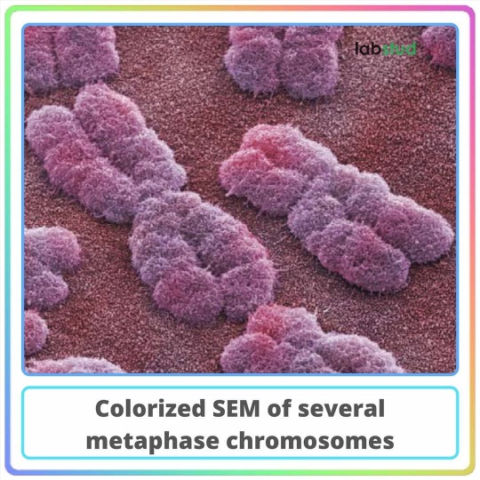
Colorized scanning electron micrograph of several metaphase chromosomes It is showing the paired identical chromatids associated loosely along their length and joined tightly at the centromere These chromatids split apart from one another in anaphase. @bylabstud via Andrew Syred/Photo Researchers, Inc. #sem #scanningelectronmicroscopy #microscopicworld #microscopy #chromosome #chromatids #telomeres #centromere #metaphase #cellbiology #cell #celldivision #cellcycle #biologyteacher #biologystudent #medstudents #biotechnology #biotechnologystudent (at Washington University Pathology Department) https://www.instagram.com/p/B65e4IPpmUZ/?igshid=ta2z7wf052zm
#sem#scanningelectronmicroscopy#microscopicworld#microscopy#chromosome#chromatids#telomeres#centromere#metaphase#cellbiology#cell#celldivision#cellcycle#biologyteacher#biologystudent#medstudents#biotechnology#biotechnologystudent
0 notes
Text
#scanningelectronmicroscope#scanningelectronmicroscopy#sem#microscopy#microscope#science#electronmicroscope#art#electronmicroscopy#sciart#biology#nature#microscopyart#design#scienceart#microscopes#preparedslides#womeninscience#micrograph#microscopio#diatomshop#diatomlab#macro#micrography#pollen#microscopic#diatomresearch#bnw#laboratory#eye
0 notes
Text

13: Digital Electron Microscopy We look forward to receiving your abstracts and your participation in the 12th World Digital Pathology & AI UCGCongress, from December 17-19, 2024 in Holiday Inn Dubai, UAE & Virtual. WhatsApp us: https://wa.me/442033222718?text= Submit your abstract here: https://digitalpathology.ucgconferences.com/digital-electron-microscopy/ #ElectronMicroscopy #DigitalMicroscopy #TEM #ScanningElectronMicroscopy #CryoEM #MicroscopyImaging #NanoImaging #HighResolutionImaging #ElectronMicrographs #MicroscopyTech #CellularImaging #MaterialsScience #Nanotechnology #BiomedicalImaging #ScienceVisualization #ElectronBeam #MicroscopyAnalysis #ImageProcessing #DigitalAnalysis #ScientificResearch
0 notes
Photo

Winged Ant #ant #creepy #creepyinsect #entemology #scanningelectronmicroscopy #blackandwhite #nanoscape #microworld #microscope #microscopy #artistsoninstagram #sciart #artandscience #scienceandart #science #art #backscatteredelectrons #unfiltered #unknown #seeingtheunseeable #electronmicroscope #electronmicroscopy #micrograph #instascience #scienceisfun🔬 #scienceisawesome #🔬#insectagram #insectalicious #insectphotography https://www.instagram.com/p/BpnF5QRhgku/?utm_source=ig_tumblr_share&igshid=cb6apv9fpr0i
#ant#creepy#creepyinsect#entemology#scanningelectronmicroscopy#blackandwhite#nanoscape#microworld#microscope#microscopy#artistsoninstagram#sciart#artandscience#scienceandart#science#art#backscatteredelectrons#unfiltered#unknown#seeingtheunseeable#electronmicroscope#electronmicroscopy#micrograph#instascience#scienceisfun🔬#scienceisawesome#🔬#insectagram#insectalicious#insectphotography
1 note
·
View note
Photo

Researcher Josh Einsle shares his typical day studying planets on the nanoscale on rockheadsciences.com #Earth #microscope #planets #space #minerals #magnetics #meteorites #laboratory #rocks #geology #physics #scanningelectronmicroscopy #engineer #crystals #careers #academics #UK
#engineer#crystals#physics#scanningelectronmicroscopy#uk#planets#careers#rocks#earth#minerals#magnetics#academics#meteorites#microscope#laboratory#space#geology
0 notes
Text
Part 2: Scanning Electron Microscopy (SEM) | Instrumentation of SEM | Electron Microscopy
https://superspunarticle.com/part-2-scanning-electron-microscopy-sem-instrumentation-of-sem-electron-microscopy/ Part 2: Scanning Electron Microscopy (SEM) | Instrumentation of SEM | Electron Microscopy https://superspunarticle.com/part-2-scanning-electron-microscopy-sem-instrumentation-of-sem-electron-microscopy/ Some tips on Content & Video Marketing. The above video post was published here. I trust that you found the above useful or of interest. You can find similar content on our blog here: superspunarticle.com/blog Please let me have your feedback below in the comments section. Let us know which subjects we should write about for you in future. #Dr.PuspendraClasses #electronmicroscopy #InstrumentationofSEM #InstrumentationofTEM #paidadvertising #payperclick #PPC #PrincipleofSEMandTEM #scanningelectronmicroscopy #searchenginemarketing #SearchEngineoptimisation #Searchengineoptimization #sem #semandtem #SEO #TEM #TransmissionElectronMicroscopy #ContentMarketingVideo
0 notes
Photo

Whoa, we're glad these guys are on our side! This scanning electron micrograph image gets up close and personal with a type of human immune cell called a 'natural killer' cell. They are a critical part of our immune systems, and help keep us safe from viral infections! 💪 📷: NIAID . . Follow @atomstalk . . . . #science #immunesystem #immunehealth #immunitysystem #immunesystemhealth #whiteblood #whitebloodcells #bloodcells #humananatomy #humanbiology #biology🔬 #microscopes #scanningelectronmicroscopy https://www.instagram.com/p/CCWCtHkj71t/?igshid=9tj10ca1uo44
#science#immunesystem#immunehealth#immunitysystem#immunesystemhealth#whiteblood#whitebloodcells#bloodcells#humananatomy#humanbiology#biology🔬#microscopes#scanningelectronmicroscopy
0 notes
Photo

i can’t focus my SEM image because i’m distracted with Batman! hahahaha he keeps appearing on the surface! 😂😂😂 #amazingadventuresofbeaujethro #batman #sem #scanningelectronmicroscope #scanningelectronmicroscopy #microscopy #electronmicroscopy #filipinoscientist #physicist #materials #materialsscience #physics #chemistry (at IMREDD)
#batman#materials#physicist#scanningelectronmicroscope#electronmicroscopy#chemistry#amazingadventuresofbeaujethro#scanningelectronmicroscopy#microscopy#physics#filipinoscientist#sem#materialsscience
0 notes
Photo

#Cytopathology, #ScanningElectronMicroscopy in Dental Studies, know more @ http://surgicalpathology.alliedacademies.com/
#pathology#surgical pathology#pathology conference#conference#congress#paris#france#cytyopathology#scanning electron microscopy
0 notes