#verilog ip core
Explore tagged Tumblr posts
Visit Tumblr Blog
Explore Tumblr blogs with no restrictions, modern design and the best experience.
Last Seen Tumblr Blogs


Fun Fact
Tumblr’s reach among the 26-to-35-year-olds in the US is 11%.
Text
Innovations in AHB DMA Controller for High-Speed Memory Access
In the rapidly evolving field of digital technology, efficient memory access remains a critical factor for system performance. At the heart of this challenge lies the AHB DMA controller, a key component designed to manage direct memory access with precision and speed. Digital Blocks has been at the forefront of innovating this technology, refining the AHB DMA controller to meet the demanding needs of modern applications.
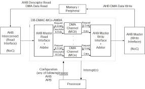
Understanding the Role of the AHB DMA Controller
The AHB DMA controller plays a pivotal role in facilitating high-speed data transfers between memory and peripherals without burdening the central processing unit. By enabling direct memory access, this controller significantly reduces latency and frees up processing power for other critical tasks.
Digital Blocks has recognised the importance of this function and invested in enhancing the efficiency and reliability of the AHB DMA controller. These innovations allow for smoother data flow and improved system responsiveness, which are essential for industries relying on high-performance computing.
Enhancements in Data Transfer Efficiency
One of the significant advancements introduced by Digital Blocks in the AHB DMA controller involves optimising data transfer protocols. By improving how the controller manages burst transfers and prioritises data requests, the new designs achieve faster throughput rates.
This optimisation ensures that large blocks of data move seamlessly between system components, reducing bottlenecks that traditionally slow down operations. The result is a system that performs consistently at high speeds, meeting the rigorous standards of applications such as multimedia processing, communication devices, and embedded systems.
Robustness and Flexibility in Design
Digital Blocks’ approach to the AHB DMA controller also emphasises robustness and adaptability. The controller now supports multiple channel operations, allowing simultaneous data transfers without conflict. This multi-channel capability is crucial for systems that require parallel processing and multitasking.
In addition, the controller design offers configurability to match specific application requirements. This flexibility means that engineers can tailor the AHB DMA controller to optimise performance according to system needs. Such customisation ensures better power management and resource allocation, contributing to overall system efficiency.
Integration with Advanced System Architectures
The continuous development of the AHB DMA controller by Digital Blocks aligns well with the trends in system architecture. Modern designs increasingly demand controllers that integrate seamlessly with advanced bus systems and processors.
By maintaining compliance with industry standards and supporting a wide range of protocols, the AHB DMA controller fits into diverse system environments. This compatibility simplifies integration, reduces development time, and lowers costs. It also ensures that the controller remains relevant as new technologies emerge.
Conclusion: Leading the Future of Memory Access
The innovations introduced by Digital Blocks in the AHB DMA controller mark a significant step forward in high-speed memory access. By focusing on efficiency, robustness, and integration, these developments provide a reliable solution for today’s demanding digital systems.

As technology continues to advance, the need for powerful memory management tools will only grow. Digital Blocks’ commitment to refining the AHB DMA controller ensures that it remains a key player in supporting the future of high-performance computing.visit our website
#ahb dma controller#axi dma ip core#ahb dma verilog#axi4 stream dma#axi dma controller ip#axi dma scatter gather#axi bridge ip core#axi dma verilog#axi stream dma#axi4 data mover
0 notes
Text
Agilex 5 E-Series with Power-Optimized Edge Performance
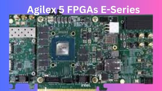
Intel Agilex 5 FGPA
Agilex 5 E-Series
Altera’s latest mid-range FPGAs, the Agilex 5 FPGAs E-Series, are now supported by the recently released Quartus Prime Software v24.1, which can be downloaded right now. Intel are happy to announce that it is now simpler than ever and completely free of charge to take use of the unmatched capability of Altera’s Agilex 5 FPGAs E-Series with the introduction of the state-of-the-art Quartus Prime Software from Altera.
Intel Agilex 5
Free Licence: Get rid of obstacles. With the help of Quartus Prime Pro Edition Software v24.1, you may use the newest E-Series devices at no cost, enabling you to innovate beyond limits!
Streamlined Design Flow: Use Quartus Prime Software to see the smooth integration of intellectual property (IP)-Centric design flow. Their easily customizable design samples streamline the process of getting started so you can concentrate on what really matters your innovative ideas.
New Embedded Processing Capabilities: Make use of the Simics simulator-supported dual-core ARM Cortex-A76 and dual-core ARM Cortex-A55 of the Agilex 5 SoC FPGA, the industry’s first asymmetric processing complex. Additionally, Agilex 5 FPGAs may be combined with the feature-rich, performance- and space-optimized Nios V soft-processor for smaller embedded FPGA applications. Additionally, they collaborate with a number of partners who provide a top-notch suite of tools to improve your FPGA and embedded development experience, including Arm, Wind River, Siemens, Ashling, MathWorks, and many more.
Comprehensive Intellectual Property (IP) Portfolio: With their tried-and-true IP portfolio for Agilex 5 FPGAs, many of which are free, you may shorten the time it takes to market. Reduce the amount of circuitry used and make design timing closure easier with hard IP solutions for PCI Express, Ethernet, and memory protocols, which also support LPDDR5. With PCS’s Ethernet 10G MAC, you can guarantee deterministic and synchronised communication, enhanced by Time-Sensitive Networking (TSN) features.
This version includes the Video and Vision Processing (VVP) portfolio IP for Agilex 5 FPGAs, which enables the entire portfolio of video solutions, as well as additional IPs supporting MIPI D-PHY and MIPI CSI-2. Begin developing your Agilex 5 FPGA designs and rely on additional validated advanced features like JESD204C IP, ORAN IP, LDPC IP, CPRI, and eCPRI among others.
Unprecedented Capabilities: Altera FPGAs may be programmed with cutting-edge capabilities like the following using the Quartus Prime Pro Edition Software v24.1.
Agilex 5 datasheet
Dashboard for Quartus Software Exploration (Preproduction)
With distinct instances of Quartus Prime software, numerous projects running concurrently may be easily coordinated and the compilation and timing results can be seen.
Fresh Features for Compilation: Generation flow of precompiled components (PCCs)Utilising the new precompiled component (PCC) generation flow during compilation, shorten the time it takes to compile synthesis.Start the Simulator using the Quartus Prime GUI.Effortlessly start simulations straight from the Quartus Prime GUI by using the handy “Tools ➤ Run Simulation” menu item. Remove the need for extra procedures to streamline your workflow and save time.
Features and Improvements of Synthesis
Use the RTL Linter Tool to convert older RTL files to Verilog/VHDL standards with ease, optimise RAM inference for better speed and resource use, and reduce warnings in error-free RTL modules to increase readability while developing.
Improved Timing Indicator
Gain more flexibility in timing analysis and SDC scripting with new scripting options; guarantee design integrity with sign-off capabilities for particular combinational loops; and learn more about timing characteristics with enhanced Chip Planner visualisation of asynchronous clock domain crossings (CDCs).
Innovations in Advanced Link Analysers
Link Builder: Use the brand-new Link Builder tool to quickly and easily build high-speed serial connections. Streamline the connection creation procedure by automatically generating schematics and importing channels and devices.
High DPI Monitor Assistance: Benefit from improved readability and display quality thanks to GUI scaling for high DPI displays and automated DPI recognition. Enjoy enhanced usability and user experience.
Enhanced Data Viewer: With improvements to the Data Viewer, analyse forward error correction (FEC) code word faults more effectively. Error outcomes may be easily interpreted and analysed for more efficient error correction techniques.
Enhancements to Simulation Time:
Easy-to-use UI for automated import of devices and channels and schematics. Agilex 7 IP offers faster simulation times with the updated Q run and FEC models.
Qualities:
R-Tile: Transaction Layer (TL) multi-channel DMA IP (AXI) up to Gen5 x16 For flexibility in incorporating third-party PCIe Switch IP, use the bypass mode. A new design example for Gen5 x4 endpoint configuration is also provided.
F-Tile: Utilising FastSIM to reduce simulation time in PIPE mode and providing Ubuntu driver support for all sample designs.increased compatibility for up to 64 embedded endpoints.For greater coverage, the Debug Tool Kit (DTK) was added to the switch IP.
Become a Part of the Community: Hua Xue, VP & GM Software Engineering, remarked, “Intel’re excited to offer Quartus Prime Software v24.1, a crucial milestone in FPGA design.”
“Now, engineers everywhere can easily access the unmatched potential of Agilex 5 FPGAs E-Series.” Quartus’s simplified design process and these cutting-edge technologies allow engineers to reach their full potential for innovation. With their state-of-the-art processing capabilities, Agilex 5 devices transform embedded FPGA applications. These are enhanced by Quartus’s vast IP portfolio, which includes a variety of solutions like Ethernet, PCI Express, memory protocols like LPDDR5, support for MIPI D-PHY, CSI-2, and a suite of video solutions, among many other IPs.
The Quartus Exploration Dashboard offers a user-friendly interface and optimization recommendations, which further improve the design exploration process. Intel’re pushing both the simplicity of use and the fast compiler technologies with Quartus v24.1’s open access to E-Series FPGAs and a simplified design pipeline to enable engineers and innovators to unleash their creativity like never before.”
Intel Agilex 5 price
Normally marketed to corporations and incorporated into bigger systems, the Intel Agilex 5 FPGAs do not have a set pricing that is made accessible to the general public. A number of variables affect the pricing, including:
Model specifics: The Agilex 5 family has two distinct series (D and E) with differing logic cell characteristics and capacities. Models with additional features will cost more.
Volume: If you buy in large quantities, you may be able to negotiate a lower price with distributors or directly with Intel.
Distributor: Price structures may vary significantly throughout distributors.
Read more on Govindhtech.com
#Agilex#intelagilex#agilex5#intelagilex5#govindhtech#FPGA#news#technews#technology#technologynews#TechnologyTrends Intel
0 notes
Link
0 notes
Text
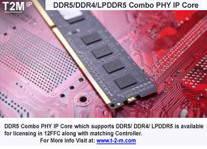
DDR5 DDR4 LPDDR5 Combo PHY IP Core
T2MIP, the global independent semiconductor IP Cores provider & Technology experts, is pleased to announce the immediate availability of its partner’s DDR5/DDR4/LPDDR5 Combo PHY IP Core in 12FFC process node with matching DDR5 Combo Controller IP Core which are silicon proven with High bandwidth and superfast data rate.
The DDR5/DDR4/LPDDR5 Combo PHY and Controller IP Core is also able to run on DDR4, DDR5, LPDDR5 modes separately. The structured yet simple design allows easy adoption into any design architecture and provides low latency and enables up to 5400MT/s throughput. There is availability of special feature of Programmable output impedance (DS) and Programmable on-die termination (ODT). Compliant with DFI version 5.0 Specification, the DDR5 Combo PHY with matching Controller can support up to 16 AXI ports with data width up to 512 bits.
The DDR5/DDR4/LPDDR5 Combo PHY IP core in 12nm FFC process technology supports varied DDR5/ DDR4/ LPDDR5 with Maximum Controller clock frequency of 675MHz, 400MHz, 600MHz resulting in maximum DRAM data rate of 5400MT/s for DDR5, 3200MT/s for DDR4 and 4800MT/s for LPDDR5 respectively. It Supports four modules for flexible configuration CA/DQ_X16/DQ_X8/ZQ. The 12FFC technology comes with added feature of ZQ calibration and supports 4 ranks by each CA module in different consideration of power consumption with an Operating Voltage of Core power of 0.8V.
The DDR5 Combo Controller IP Core is full-featured, easy-to-use, synthesizable design, compatible with DDR5 JESD79-5 and JESD79-5 specification. It is compliant with different clock frequency for DDR5, DDR4 and LPDDR5. It also supports PHY internal auto decision and has additional features such as Maximum Power Saving Mode (MPSM), Precharge Command modes, Error Checking, and correction (ECC), reordering of transactions for higher performance and Self-Refresh and Power Down operation. It is able to support up to 64GB device density and X4, X8, X16 device types These IP Cores functionalities are verified in NC-Verilog simulation software using test bench written in Verilog HDL, which are provided with the IP Core delivery.
The DDR5 Combo PHY IP core along with the DDR5 Combo Controller IP Core have been used in semiconductor industry’s Enterprise computing, storage area networks, Embedded systems, Graphics devices and other Consumer Electronics…
In addition to DDR5 IP Core, T2M ‘s broad silicon Interface IP Core Portfolio includes other USB, HDMI, Display Port, MIPI (CSI, DSI, UniPro, UFS, Soundwire, I3C), PCIe, 10/100/1000 Ethernet, V by One, programmable SerDes, SD/eMMCs, Serial ATA and many more, available in major Fabs in process geometries as small as 7nm. They can also be ported to other foundries and leading-edge processes nodes on request.
Availability: These Semiconductor Interface IP Cores are available for immediate licensing either stand alone or with pre-integrated Controllers and PHYs. For more information on licensing options and pricing please drop a request / MailTo
About T2M: T2MIP is the global independent semiconductor technology experts, supplying complex semiconductor IP Cores, Software, KGD and disruptive technologies enabling accelerated development of your Wearables, IOT, Communications, Storage, Servers, Networking, TV, STB and Satellite SoCs. For more information, please visit: www.t-2-m.com
2 notes
·
View notes
Text
What is a SPI Controller IP core?
The Serial Peripheral Interface (SPI) permits fast synchronous serial information exchange between microprocessors / microcontrollers and peripheral devices. The SPI-MS center can work either as a Master or a Slave SPI bus device. Digital Blocks offers full highlighted SPI Controller IP Verilog Cores, with discharges containing Master/Slave, Master-and Slave-just capacities, and QSPI Flash Memory Controller Verilog IP Cores. QSPI Flash Memory Controllers get to QSPI Flash by CPU with choice for Execute-In-Place (XIP) and boot.

Highlights of SPI Controller IP core:
• Support for both SPI Master and Slave.
• Multi Master Support.
• In Master Mode – bit rate created is System Clock/2.
• In Slave Mode – bit rate upheld is ≤ System Clock/8.
• Programmable SCK Phase and Polarity.
• Supports Repeated Start and Fast Read Operation.
• Transaction Layer actualized in HDL Source code too.
• Programmable interior information way width from 1 byte to 64 bytes.
• Technology free HDL Source code.
• Supports all FPGA gadgets.
• Well demonstrated IP against numerous SPI gadgets.
SPI Controller Reference Designs and Evaluations:
For FPGA configuration groups, we offer AMBA Interfaces to CPUs in all Master/Slave, Master- only and Slave-only discharges. For Altera® FPGAs, we furthermore offer the Avalon Interface to the Nios® II inserted processor. All SPI Controller IP Cores are accessible in Verilog RTL or, for bring down costs, Altera® or Xilinx® net list groups.

For ASIC, ASSP, Custom IC configuration groups, we offer AMBA Interfaces to CPUs in all Master/Slave, Master-only, and Slave-only discharges. All SPI Controller IP Cores are accessible in Verilog RTL. For organizations first seeking after FPGA emulation, Digital Blocks services will completely help. To take in more about the SPI Controller IP Core please contact Digital Blocks @ https://www.digitalblocks.com/spi-ip-core-reference-design.html
0 notes
Text
The Arty RISC-V Computer
Part 3: Finding a RISC-V core for the Arty
The Xilinx Arty A7 is a popular, low-cost Artix-7 FPGA Development Board designed for makers and hobbyists, with the capacity to run a soft processor. It includes a range of Input/Output (I/O) devices, such as LEDs, 7-segment displays, flash memory, SDRAM, and expansion connectors for PMOD modules. PMODs enable a range of additional hardware to be added, such as a VGA output, OLED display, switches, and A/D converters, which can be driven directly by the Artix-7 FPGA.

Figure 3. The Xilinx Arty A7 FPGA board
The other great benefit of the Arty is that it includes Vivado Design Studio (the license is device locked to the Arty), a software suite produced by Xilinx for synthesis and analysis of Hardware Development Language (HDL) designs. Vivado enables developers to synthesize (compile) their designs, perform timing analysis, examine RTL diagrams, simulate a design's reaction to different stimuli, and configure the target device with the programmer (see en.wikipedia.org/wiki/Xilinx_Vivado).
After I chose the Arty board for this project, the next step was to find an existing RISC-V processor design which could be loaded onto it. The first stop was the SiFive website, which has a downloadable Xilinx bitstream file containing a basic RISC-V SoC for the Arty board. In addition, SiFive offers their FreedomStudio development suite, which makes it easy to write programs in C, and upload them to the SoC.
I signed up at the SiFive website, downloaded and programmed the Arty with the RISC-V SoC bitstream, and LED0 changed colors to indicate the processor was running. Fantastic! Then I downloaded and installed FreedomStudio (based on Eclipse), and compiled the simple UART example project bundled with it. I uploaded it directly from FreedomStudio, and watched my serial terminal program dump out a text banner of the SiFive logo. Great stuff!

Figure 4. The SiFive logo
I thought I’d also be able to write RISC-V assembly language (ASM) code with FreedomStudio, but this doesn’t seem to be available. It is possible to view the assembler code for a compiled C program in a panel in FreedomStudio, but it’s not the ASM bare metal level of access I was hoping for. That was a bit disappointing. Maybe they’ll add this to a future version.
Now I wanted to have a closer look at their RTL source code, to see how they had built the RISC-V processor in VHDL/Verilog. I also wanted to add my own peripherals, such as the VGA output. I signed up on their website for access, and my request was quickly granted. I then downloaded the RTL source code, only to discover it was obfuscated (ie. mixed up to make it unreadable by humans). There were some fixed peripherals, and very small amounts of on-SoC RAM, effectively making it impossible to extend in the way I’d planned. Another disappointment, though I guess understandable, as they are selling their IP on a commercial basis.
The second promising RISC-V implementation I found was open source, and available on Github. It’s called the ‘Potato’ RV32I processor, “A simple RISC-V processor for use in FPGA designs”, and maintained by Kristian Klomsten Skordal (see github.com/skordal/potato). Kristian provides excellent instructions for setting up the Potato processor on the Arty board, and in his documentation suggested using the RISCV GNU toolchain repository site to build and install a 32-bit RISC-V toolchain.
The RTL code was in VHDL (my preferred language), using the Wishbone interconnect - I would have preferred AXI, but Wishbone is good too, and it’s open source. It looked like I was finally able to do everything I wanted to with a RISC-V SoC for Arty!
1 note
·
View note
Text
#ahb dma controller#axi dma ip core#axi dma scatter gather#axi bridge ip core#axi dma verilog#axi dma controller ip#axi stream dma#ahb dma verilog#axi4 stream dma#axi4 data mover
0 notes
Text
JPEG Resize on-demand: FPGA vs GPU. Which is the fastest?
https://www.fastcompression.com/blog/jpeg-resize-on-demand-fpga-vs-gpu-performance-comparison.htmHigh performance image processing is essential task for web applications. It's not a rare situation when companies need to process hundreds of millions images every day. In some services that number could reach several dozens of billions images per day. Here we review available hardware and software solutions for such tasks. We will not consider CPU-based implementations here and focus on FPGA vs GPU as the fastest hardware for parallel computations.
Internet traffic is increasing by ~25% annually (according to white paper from CISCO, see below) and images take considerable part of that data. Many companies are handling huge volumes of images in their data centers:
Cloud storage, CDN
Mobile instant messaging
Images for social networks, image social platforms, cloud albums, photo hosting centers
User-Generated Content platforms (UGC)
E-Commerce platforms
Market demand
Users generate more images and video data every day
User devices have higher resolution in capture and display
Users strive to better viewing experience
Better image quality and QoS
Customers demand instant access to the resource (reduced latency)
Challenges
Huge consumption of computational and storage resources
Server and storage performance is not enough
As a task for performance and latency comparison for FPGA vs GPU at image processing, we will consider JPEG Resize on-demand which is widely utilized in web applications. Total number of JPEGs in the world is absolutely huge and it's significantly increasing every day. That's why companies spend quite a lot on storages for these pictures and on hardware/software for image processing. The simplest approach is to store the same JPEG picture at several different resolutions and to send an image which is slightly bigger at each request. Such an approach can't match desired image resolution exactly. To cut the expences on storage and to respond to user faster, we can resize JPEG images in realtime according to necessary dimensions to accomplish full match with the requirements of user's device. In that case we need to store at datacenter just one original picture which will be processed according to individual request parameters. That idea about on-demand resize for JPEG images is not new and it has already been implemented in several internet services on CPU, GPU and FPGA.
Image processing pipeline for JPEG Resize on-demand
JPEG Decoding
Resizing and Cropping
Sharpening
Color profile handling
JPEG Encoding
That pipeline consists of different algorithms and we could hardly implement batch processing here for the whole pipeline, as soon as final dimensions are different, images could have different subsampling, individual quantization tables and Huffman tables. It means that we have to process these algorithms sequentially, though still there is a possibility to get a boost from batch mode. Most of the time in the pipeline is spent on JPEG Decoding, so we could implement batch just for JPEG decoding. We can prepare images for future batching by utilizing the same subsampling, quantization tables and Huffman tables. File size will increase a little bit, but we will get an opportunity to accelerate JPEG decoding.
Image Processing on FPGA
FPGA (Field Program Gate Array) is a specialized reconfigurable hardware which could be also utilized for fast image and video processing. This is very complicated approach for programming and FPGA engineers should know quite a lot: hardware architecture, Verlog or VHDL language, Intel (Altera) or Xilinx development tools, etc. Total understanding of hardware functioning is a must, so not everyone could do that. Still, that approach is evolving rapidly and there are some outstanding results in that field.
FPGA-based solutions posess some features which could hardly be beaten: hardware-based computations are usually very fast, the hardware could have very low dimensions and it could have extremely low power consumption. These are indispensible conditions for many embedded applications. In comparison with FPGA, any CPU or GPU-based solutions have bigger dimensions and need more power for processing with the same performance.
Despite the fact that FPGA-programming is very complicated, there are quite a lof of imaging solutions which are based on FPGA/ASIC hardware. Moreover, neural networks have already been implemented on FPGA and that hardware platform is considered to be very promising for Deep Learning and Artificial Intelligence tasks. Currently, neural networks are much more easier to implement on GPU, than on FPGA. But FPGA is a competitive solution, though at the moment it requires super high skills to work with.
Some frame grabbers have built-in library for internal FPGA-based image processing. Silicon Software framegrabbers (now belongs to Basler company) have such a feature and this is the way to implement FPGA-based image processing for camera applications without writing any code on VHDL or Verilog. This is important task to ensure faster than realtime image processing on FPGA for high speed and high performance cameras.
CTAccel solutions on Intel FPGAs
CTAccel company is based in Hong Kong and Shenzhen. This is a team of FPGA professionals with solid record of achievments in FPGA design, hardware/software co-design, system optimization and software engineering. The core team of CTAccel comes from the FPGA team of Clustertech Ltd.
CTAccel Image Processing Solutions
CTAccel Image Processor (CIP) effectively accelerates the following image processing/analytics workflows:
Thumbnail Generation/Transcoding
Image processing (sharpen/color filter)
Image analytics
CIP includes the following FPGA-based accelerated functions:
Decoder: JPEG
Pixel processing: Resize/Crop
Encoder: JPEG, WebP, Lepton
Software compatibility with OpenCV, ImageMagick and Lepton
CIP Image Processing Pipeline (image from that PDF)
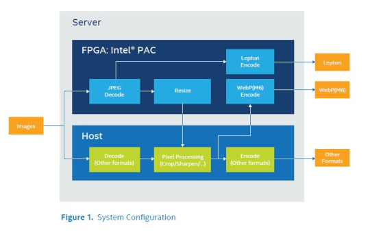
That diagram for suggested image processing pipeline shows that Crop, Sharp and Color conversions are implemented on Host CPU, not on FPGA. In that case we get combined heterogeneous solution, where image processing is done both on FPGA and CPU. This leads to additional load for CPU.
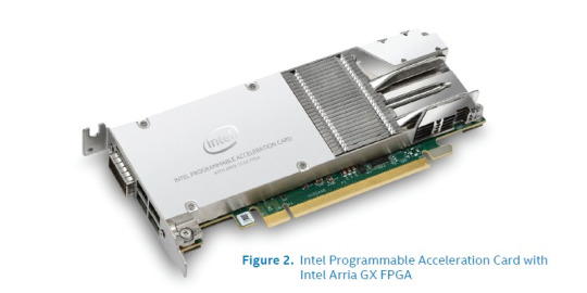
Intel FPGA board (image from that PDF)
The CIP accelerator features an Intel® Programmable Acceleration Card (PAC) with Intel Arria® 10 GX FPGA.
Performance evaluation for CTAccel CIP solution on Intel PAC
JPEG Resize solution from CTAccel for Intel® Programmable Acceleration Card can do JPEG decoding, image resize and JPEG encoding. This is the screenshot for Real-world customer use case from CTAccel site:
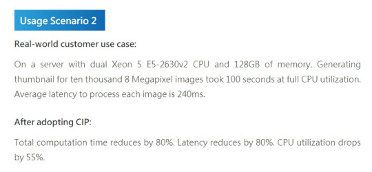
8 MPix image is converted to thumbnail on Intel Xeon E5-2639 v2 CPU within 10 ms (100 sec / 10,000 images), which means that on CTAccel CIP that image could be processed within 2 ms (total computation time 10 ms reduced by 80%). For further comparison we can conclude that 3 MPix jpeg image could be resized on Intel PAC with CTAccel CIP within 0.8 ms which is equal to 1250 fps (frames per second).
Averaged latency for 3 MPix image processing on FPGA is the following: (240 ms * (100 - 80) / 100 * 3 / 8 = 18 ms. This actually means that FPGA is processing around 18 / 0.8 = 22 images at the same time. It looks like a batch mode for JPEG decoding on CIP has already been implemented.
Unfortunately we don't have full info about parameters for that pipeline. Nevertheless, we can expect that original compressed image should be close to visually lossless compression. "Generating thumbnails" approach means that final image resolution is very small, so applied resize takes less time and output JPEG encoding takes almost no time. In real-life case of JPEG Resize on-demand we need to fit resolution of smartphone screen, and this is more computationally intensive (that scenario was used for tests with NVIDIA Tesla T4 GPU). Still, these performance results could be a ground to make indirect comparison with benchmarks on NVIDIA Tesla T4. To the best of our knowledge, pricing for Intel PAC board and NVIDIA T4 is comparable.
XILINX

Xilinx Alveo, a portfolio of powerful accelerator cards designed to dramatically increase performance in various tasks. Xilinx® Alveo™ U280 Data Center accelerator cards are designed to meet the constantly changing needs of the modern Data Center. Built on the Xilinx 16nm UltraScale™ architecture, Alveo U280 ES offers 8 GB of HBM2 410 GB/s bandwidth to provide high-performance, adaptable acceleration for memory-bound, compute intensive applications including database, analytics, and machine learning inference. The U280 ES acceleration card includes PCI Express 4.0 support to leverage the latest server interconnect infrastructure for high-bandwidth host processors. And like all Xilinx technology, customers can reconfigure the hardware, enabling them to optimize for shifting workloads, new standards and updated algorithms without incurring replacement costs.
Alveo accelerator cards are adaptable to changing acceleration requirements and algorithm standards, capable of accelerating any workload without changing hardware, and reduce overall cost of ownership.

Xilinx Alveo U280 Data Center accelerator card (image is taken here)
There are some libraries which allow to implement image processing algorithms on FPGA via C++ instead of Verilog/VHDL, though finally VHDL code will be generated. Xilinx Video and Image Processing Pack is an example how to do that. It includes full licenses to the following LogiCORE IP cores:
Chroma Resampler
Color Correction
Color Filter Array Interpolation
Gamma Correction
Image Edge Enhancement and Image Noise Reduction
On-Screen Display
Video Deinterlacer
Video DMA
Video Timing Controller
The Xilinx Video and Image Processing Pack provides bundled licensing option for all of the LogiCORE™ IP blocks. Video processing blocks provide optimized hardware implementations for video scaling, on-screen display, picture-in-picture, text overlay, video and image analysis and more. Image processing blocks enable pre-processing of images captured by a color image sensor with a Bayer Color Filter Array (CFA), correcting defective pixels, interpolating missing color components for every pixel, correcting colors to adjust to lighting conditions, setting gamma to compensate for the intensity distortion of different display devices and more.
CTAccel on Virtex UltraScale+ VCU1525
The above set of image processing features from Xilinx LogiCORE IP cores is not enough to accomplish the task of JPEG Resize on-demand. That task was solved on Xilinx FPGA hardware by CTAccel company, as in the case with Intel FPGA. That solution from CTAccel on Xilinx is utilized by Huawei Cloud for FPGA Image Transcoding Acceleration on Virtex VU9P to provide easy-to-use and cost-effective image transcoding services. For the task of thumbnail generation (which is alike the task of JPEG Resize on-demand, but more simple), published benchmarks for performance and latency are the same as for Intel FPGA solution - this is 0.8 ms for 3 MPix jpeg image. It should be noted that the same CTAccel CIP solution can work on Xilinx Alveo accelerator cards as well.
Xilinx VCU1525 developer board (image is taken here)
GPU Image Processing on NVIDIA CUDA
GPU architecture was initially created for image display and finally it was transformed for parallel computations. Image processing could be considered as native task for GPU, though we need SDK not to program GPU at low level. There are quite a lot of such SDKs with sofisticated set of features.
Full set of features for JPEG resize on demand exists at Fastvideo Image Processing SDK. That SDK contains wide variety of image processing modules which show very high performance at all NVIDIA GPUs, starting from Jetson to high-end Quadro and Tesla products. Highly optimized modules show just exceptional results. For many features the performance is much higher that bandwidth of PCIe Gen3 x16. This is important issue to offer fast solution, particularly for JPEG resize on demand.
That solution has been heavily tested for years and this is the proof of its reliability in the taks of JPEG Resize on-demand. Several high-load internet services have been utilizing that software and total number of processed JPEGs exceeds several quadrillions. In comparison with recently developed FPGA-based solutions it looks much more reliable.
Fastvideo Image Processing SDK on NVIDIA T4 can do decode-resize-sharp-encode at 1.2 ms for 3 MPix image resize which is around 800 fps, but this is the result without batch mode. As soon as image resize on GPU takes small part of that time, we see that performance on JPEG Decoder is the key to achieve maximum speed for that task. Usually resized image has smaller resolution and output JPEG Encoder can process it very fast. In general, GPU JPEG Encoder is much faster than GPU JPEG Decoder, that's why JPEG decoding is the bottleneck for that task.
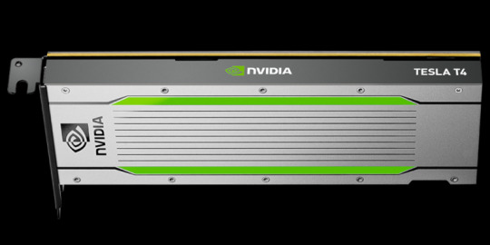
Despite the fact that we haven't yet implemented our own batch mode for JPEG Resize on-demand, there is an opportunity to increase GPU occupancy with CUDA MPS on Linux. CUDA MPS allows to utilize NVIDIA Hyper-Q technology in multi-process environment and this is the way to get much better performance if GPU is underutilized (this is exactly our case). We have run 4 processes of JPEG Resize on-demand on NVIDIA T4 and have achieved significant speedup with CUDA MPS. We've got final performance 2200 fps with CUDA MPS on NVIDIA Tesla T4.
The feature of FPGA partial reconfiguration doesn't bring any additional benefits in comparison with GPU solutions for high performance image processing tasks. Basically, the performance is defined by the hardware and software. And if we need to run any other task on the same hardware, we just need to load another software from available image processing modules. In the case with GPU, this is actually a question about availability of necessary modules in the software. Fastvideo Image Processing SDK has great variety of such modules and it can also work with any other third-party SDK, so the choice of available software features for CUDA image processing on Tesla T4 is impressive.
It should be noted that currently, versatility of GPU is much more profound in comparison with FPGA. NVIDIA GPUs have a lot of libraries which help developers to build their applications. And the idea of utilizing COTS (Commercial Off-The-Shelf) is very handy. GPU and FPGA have totally different architectures and that's why their "killer applications" are also quite different. NVIDIA, Intel and Xilinx invest a lot into their software, hardware, infrastructure, community and try to promote their solutions at full extent. They do compete everywhere and NVIDIA is now succeeding with implementation of embedded solutions on Jetson platform, though embedded solutions were always the main market niche for FPGA/ASIC. Intel and Xilinx are moving towards DL/AI to compete with NVIDIA as well.
Conclusions
We have published available results for GPU vs FPGA performance and latency for JPEG Resize on-demand task. That comparison is indirect because we have benchmarks for different scenarios: for FPGA this is thumbnail generation case for JPEG images, for GPU this is standard JPEG resize to most frequently used resolution which was acquired from statistics.
Achieved performance for the above tasks look very good in both cases: NVIDIA Tesla T4 result is around 2200 fps for JPEG Resize with CUDA MPS. Intel/Xilinx result is around 1250 fps for thumbnail generation with internal batch decoding, which is more simple task because it requires less computations. We can see that NVIDIA Tesla T4 significantly outperforms Intel/Xilins FPGA boards and we need to bear in mind that FPGA benchmarks were received in simplified test.
Computational latency in these tasks for NVIDIA Tesla T4 is 2-3 ms, for FPGA this is 18 ms.
FPGA dimensions and power consumption are not vitally important for JPEG Resize on-demand task. FPGA boards look like GPU boards and their dimensions are the same, though power consumption is still less for FPGA-based solutions which have 20W - 40W per FPGA card and 70W for NVIDIA Tesla T4.
Ease of programming is also looks alike, because mostly developers are utilizing high-level SDKs. If we have a look at low-level programming, then FPGA is much more complicated to handle.
Partial Reconfiguration and flexibility are essential benefits of FPGA, but for the current task they are not really important.
Reliability of GPU-based solution is higher due to long-term presence on the market.
Both GPU and FPGA could be utilized for other tasks, including DL/AI applications.
GPU-based solutions are basically software implementations, though FPGA solutions imply that there is non-standard hardware to work with. This is a great advantage of NVIDIA GPUs - they are commodity things. At the moment we can't call FPGA-based boards from Intel and Xilinx as commodity things yet.
NVIDIA, Intel (Altera), Xilinx, CTAccel, Fastvideo are great companies which move progress forward and create impressive software and hardware solutions for high performance applications.
What we finally get
GPU and FPGA high-performance processing capabilities offers the following benefits:
Increased image processing throughput
Reduced TCO
Reduced computational latency
Reduced size of cluster or less total number of servers
Low CPU utilization
Better user experience and QoS:
Less time to wait for image loading
Less power consumption on users's device
Less traffic due to optimal image resolutions
Better image quality (no local image resize on user's device)
Links
Cisco Visual Networking Index: Forecast and Trends, 2017–2022 White Paper (Internet traffic growth estimation)
JPEG Resize on-demand on NVIDIA Tesla V100 with Fastvideo software
Accelerating JPEG, WebP and Lepton decoding, encoding and resizing on Intel® Xeon®-based servers by offloading all functions to the Intel FPGA.
Xilinx Alveo U200, U250 and U280
Xilinx Video and Image Processing Pack
NVIDIA Tesla T4 specification
Fastvideo Image Processing SDK for NVIDIA Tesla GPUs
Jpeg2jpeg Acceleration with CUDA MPS on Linux at NVIDIA Quadro GV100
Original article see at:
0 notes
Photo

Display Controller IP
Digital Blocks Display Controller IP Cores can help ASIC/FPGA design teams with system implementations in Medical, Manufacturing, Aerospace/Defense, Automotive, Computer, Monitor, Consumer, AR/VR Headsets, IoT, Wearables, Signage, Gaming, Broadcasting, and Test Instrumentation.Visit us https://www.digitalblocks.com/ip-cores-tft-lcd-display-controller-verilog-ip-core.html
0 notes
Text
PCIe 5.0 SerDes PHY Controller IP Cores For All High-End Serial Connect Interfaces In Advanced SoCs
T2MIP, the global independent semiconductor IP Cores provider & Technology experts, is pleased to announce the immediate availability of its partner’s PCI-SIG compliant PCIe 5.0 Serdes PHY IP Cores in 12FFC process nodes with matching PCIe 5.0 Controller IP Core which are silicon proven with High bandwidth and superfast data transfer speed.
The PCIe 5.0 PHY and Controller IP cores supports the PCI 5.0 Specification, compliant with PIPE 5.1. The structured yet simple design allows easy adoption into any design architecture. Lower power consumption is achieved due to support of additional PLL control, reference clock control, and embedded power gating control. The PHY and Link Layer comes with backward compatibility support for parallel interface: 16/32- bit (Gen5/4), 10/20-bit (Gen3/2/1).
The PCIe SerDes PHY and Digital Controller IP Cores provides minimal latency and superfast isochronous data transfer. The PCIe 5.0 SerDes PHY IP Core in 12nm FFC process technology supports varied data transfer rates of 2.5 GT/s, 5.0 GT/s, 8.0 GT/s, 16.0 GT/s and 32GT/s with four (x4) physical lane width.
The 12FFC technology comes with added feature of built-in EYE-monitor and EYE checker, dual-port PLL with LC tanks and a 3-tap FFE for TX preset. Gated power for lowest leakage in L1.2 low power mode, Auto power saving for short reach and Configurable low power mode setting makes the PHY widely applicable for various scenarios under different consideration of power consumption with an Operating Voltage of 0.8V and 1.2V. ��
PCIe 5.0 Controller IP Core provides full PCIE Controller functionality with Root Complex and Endpoint BFM modes. It supports queuing for 8 configurable Virtual Channels and multi-function Configurable TC to VC queue mapping. Speed and Link Width negotiation, polarity inversion, and lane-to-lane skew Configurable timers and timeouts allows for high controllability and Scaled Flow Control. Emergency Power Reduction State allows for an advanced power management system.
These IP Cores functionalities are verified in NC-Verilog simulation software using test bench written in Verilog HDL, which are provided with the IP Core delivery. The PCIe 5.0 SerDes PHY IP core along with the PCIe 5.0 Controller IP core have been used in semiconductor industry’s Enterprise computing, storage area networks, Wireless and mobile devices, automotive, IoT, Embedded systems, Graphics devices and other industrial uses…
In addition to PCIe IP Cores, T2M‘s broad silicon Interface IP Core Portfolio includes other USB, HDMI, Display Port, MIPI (CSI, DSI, UniPro, UFS, Soundwire, I3C), DDR, 10/100/1000 Ethernet, V by One, programmable SerDes, SD/eMMCs and many more, available in major Fabs in process geometries as small as 7nm. They can also be ported to other foundries and leading-edge processes nodes on request.
3 notes
·
View notes
Text
FPGA Prototyping by SystemVerilog Examples - Pong P. Chu
FPGA Prototyping by SystemVerilog Examples Xilinx MicroBlaze MCS SoC Edition Pong P. Chu Genre: Electrical Engineering Price: $89.99 Publish Date: May 4, 2018 Publisher: Wiley Seller: John Wiley & Sons, Inc. A hands-on introduction to FPGA prototyping and SoC design This is the successor edition of the popular FPGA Prototyping by Verilog Examples text. It follows the same “learning-by-doing” approach to teach the fundamentals and practices of HDL synthesis and FPGA prototyping. The new edition uses a coherent series of examples to demonstrate the process to develop sophisticated digital circuits and IP (intellectual property) cores, integrate them into an SoC (system on a chip) framework, realize the system on an FPGA prototyping board, and verify the hardware and software operation. The examples start with simple gate-level circuits, progress gradually through the RT (register transfer) level modules, and lead to a functional embedded system with custom I/O peripherals and hardware accelerators. Although it is an introductory text, the examples are developed in a rigorous manner, and the derivations follow the strict design guidelines and coding practices used for large, complex digital systems. The book is completely updated and uses the SystemVerilog language, which “absorbs” the Verilog language. It presents the hardware design in the SoC context and introduces the hardware-software co-design concept. Instead of treating examples as isolated entities, the book integrates them into a single coherent SoC platform that allows readers to explore both hardware and software “programmability” and develop complex and interesting embedded system projects. The new edition: Adds four general-purpose IP cores, which are multi-channel PWM (pulse width modulation) controller, I2C controller, SPI controller, and XADC (Xilinx analog-to-digital converter) controller. Introduces a music synthesizer constructed with a DDFS (direct digital frequency synthesis) module and an ADSR (attack-decay-sustain-release) envelope generator. Expands the original video controller into a complete stream based video subsystem that incorporates a video synchronization circuit, a test-pattern generator, an OSD (on-screen display) controller, a sprite generator, and a frame buffer. Provides a detailed discussion on blocking and nonblocking statements and coding styles. Describes basic concepts of software-hardware co-design with Xilinx MicroBlaze MCS soft-core processor. Provides an overview of bus interconnect and interface circuit. Presents basic embedded system software development. Suggests additional modules and peripherals for interesting and challenging projects. FPGA Prototyping by SystemVerilog Examples makes a natural companion text for introductory and advanced digital design courses and embedded system courses. It also serves as an ideal self-teaching guide for practicing engineers who wish to learn more about this emerging area of interest. http://bit.ly/2XjoKFG
0 notes
Photo

Axi Dma Controller for CPU Programming ..
Digital Blocks DMA Controller IP Cores offer a flexible CPU programming interface and high-performance transfer rates with leading AMBA Interconnects and standard or customized peripheral interfaces. Digital Blocks DMA Controllers are feature-rich with Multi-Channel, Scatter-Gather capability with IP releases targeting CPU AXI/AHB backbone DMA Engines, PCI Express DMA, or Peripheral high/low data-rate DMA transfers. More can be viewed @ https://www.digitalblocks.com/dma.html
0 notes
Text
No, Hackers Didn’t Just Steal the ‘Source Code’ to AMD’s Big Navi or Xbox Series X GPUs
Two days ago, we covered news from AMD that the company had suffered an IP breach. We now know more about what was taken from the company and how serious the theft is — or more appropriately, isn’t.
At first glance, the news looks bad. The data in question is supposedly for Big Navi and Arden, the codename for the Xbox Series X GPU. Given how important both of these products are to AMD’s future, theft of their underlying core technology would be quite damaging.
WCCFTech has published a story — corroborated by certain sources ExtremeTech has spoken to — arguing that this IP theft is, while serious by its very nature, didn’t actually get the thief all that much. What was reportedly stolen were some Verilog files with information on how to implement a specific GPU function. If you don’t know what Verilog is, it’s a Hardware Description Language (HDL). You could say that a GPU or CPU is “written” in Verilog, and that’s where all the statements about AMD having had a “source code” theft are coming from. It’s not even clear the Verilog files could be useful to a third party; they’re reportedly built on a proprietary schematic that’s only compatible with AMD’s internal design language in the first place.
The important takeaway is this: There’s no way to build a product based on what was stolen and the data cannot be used to reverse engineer product performance. It might be possible to derive some high-level specification data from the full file list, but since most or all of this information is public, there’s not a lot of reason to do so. There are no known security implications from the theft at this time, though there is a slim chance that there might be an exploitable bug in the functions that were stolen. This is more-or-less a given: While we haven’t talked about security audits lately, auditing software (and Verilog is software) is an intensely time-consuming process.
We are watching the story as it develops, and obviously AMD has a very good reason to downplay the significance of what happened, but thus far everything points in the same direction: The idiot trying to extort $100M out of AMD doesn’t realize that he’s sitting on something worth much less money. Given how many people are currently sitting at home twiddling their thumbs, law enforcement would probably be glad to have something to do.
Even if it were possible for someone to buy this IP and build something off it, it wouldn’t be a smart move. You can bet AMD would be keeping a sharp eye on the horizon for any company shipping a new consumer part with conspicuously crimson capabilities. While it might be fair to say the hacker took “some” source code for these GPU families, there’s no evidence they got away with “the” source code in the manner required to reverse engineer confidential capabilities or improve a competitor product.
Now Read:
AMD Targets Mobile Core i9 With Ryzen 9 4900HS: 8 Cores, 16 Threads, Just 35W
Intel Is Still Fighting the EU Over Its Anti-Competitive Actions Against AMD
AMD Analyst Day 2020: Zen 3, Infinity Fabric 3, and 3D Packaging
from ExtremeTechExtremeTech https://www.extremetech.com/computing/308335-no-hackers-didnt-steal-source-code-amd-big-navi-xbox-series-x-gpus from Blogger http://componentplanet.blogspot.com/2020/03/no-hackers-didnt-just-steal-source-code.html
0 notes
Text
FPGA Market to Reach US$9,734.4 mn by 2020
A FPGA is an integrated circuit or semiconductor device used to implement logical function that an application-specific integrated circuit (ASIC) could perform, but the ability to update the functionality after manufacturing offers advantages such as re-programming in the field for rapid prototyping and debugging for many applications. FPGAs use programmable routing channels and pre-built logic blocks for implementing custom hardware functionality, depending upon the embedded system developer configuring these devices. FPGAs are programmed and configured using Hardware Description Language (HDL) such as VHDL and Verilog. Medical imaging equipment demands numerous processing requirements based on the definite data acquisition principles and algorithms used in image processing. High performance computing capabilities in imaging equipment is one of the major factors contributing to the growth of high-end processors and field-programmable gate arrays. The advantages of FPGA in digital signal processing (DSP) over other processors make it a feasible alternative for most imaging equipment such as computerized tomography (CT) and positron emission tomography (PET) machines. Though FPGAs have begun to replace DSP in most applications, there exists a trend to use them as co-processors. General diagnostic imaging devices include X-rays, mammography equipment, ultrasounds, CT scanners, MRIs, and nuclear medicine imaging.
The automobile market continues to witness a proliferation of electronic content due to governmental guidelines on pollution, security and safety regulations, and the ongoing oil crisis. Furthermore, increasing luxury features in automobiles require efficient solutions, thereby boosting demand in the FPGA market. Moreover, rising fuel prices in the global market have resulted in demand for electric and hybrid vehicles, which in turn is expected to drive FPGA content in automobiles. In Europe, regulations such as the Antilock Braking System (ABS), Electronic Stability Program (ESP), and electronically controlled independent suspension are expected to generate substantial revenues in the near future. North America dominates the automobile market; however, Asia Pacific has significant potential to become the key contributor to FPGA revenues. FPGA is used in automobiles for various applications including driver assistance, rear-view camera, forward camera, surround-view camera, infotainment, and electric vehicles.
Read Report Sample @
https://www.transparencymarketresearch.com/sample/sample.php?flag=S&rep_id=1405
High performance computing in the financial sector is continuously challenged by rising demand for capability to process larger volumes of data with faster results. FPGA can significantly increase the throughput of systems and decrease data center load. As a result, FPGAs are extensively adopted in mainstream embedded computing to build complex mission-critical systems. FPGA’s underlying programmable architecture is being used for numerous purposes in the financial sector including real-time trading, performance arbitrage, risk analysis, and ex-post factor data analysis. Companies such as Fixnetix have launched ix-eCute, the pre-trade risk FPGA microchip for ultra-low latency implementation for Canada. In addition, companies such as Enyx are focusing on software and IP cores for optimizing FPGAs for the trading floor. Accelize is serving the finance industry with its ultra-low latency FPGA network platforms. Thus, the FPGA market is expected to witness substantial growth in the financial domain over the forecast period.
Telecom is the largest application segment for FPGA. Other applications include automobile, consumer electronics, industrial, data processing, military and aerospace, and medical industries. Unlimited demand for bandwidth in wireless networks is driving this market. In addition, increase in demand for smartphones and tablets are boosting the market. FPGA is widely used in imaging equipment and the automobile industry to enable high performance computing abilities. This is contributing to growth of the market.
Read Report Brochure @
https://www.transparencymarketresearch.com/sample/sample.php?flag=B&rep_id=1405
‘Accumulating 3D ICs with FPGA, processors, SerDes, and memory controller, and other part offering DDR memory is expected to open up opportunity to the market growth during the forecast period. Also, there is major demand for FPGA for low power, cost-sensitive, and space-constrained applications. With increase in number of industries operating in industrial, automotive, and telecom sector, Asia Pacific dominates FPGA market, followed by the U.S. and Europe.
Major market participants profiled in this report include Xilinx Inc., Altera Corporation, Lattice Semiconductor Corporation, Microsemi Corporation, among others.
0 notes
Text
Logic Design Lead
Location: Austin, TX / Hudson, MA / Sunnyvale, CA FullTime Opportunity Job Description: 9+ years of experience and Participated in 2-3 SoC projects Must have extensive experience in Micro-architecture design at IP/Subsystem level Experience in any of the following domain is highly desirable: o HBM o PCIe Gen3/4 o Any high speed chip to chip interconnect o Multi core processor architecture and SIMD processors Extensive experience in SoC RTL coding (Verilog or System-Verilog). Experience in RTL Code Linting and CDC checks. Experience in RTL integration using Industry standard tools, is an added advantage Experience in low power design techniques Good unders...
Source: https://www.jobisite.com/sj/id/9046150-Logic-Design-Lead-
0 notes
Text
Logic Design Lead
Location: Austin, TX / Hudson, MA / Sunnyvale, CA FullTime Opportunity Job Description: 9+ years of experience and Participated in 2-3 SoC projects Must have extensive experience in Micro-architecture design at IP/Subsystem level Experience in any of the following domain is highly desirable: o HBM o PCIe Gen3/4 o Any high speed chip to chip interconnect o Multi core processor architecture and SIMD processors Extensive experience in SoC RTL coding (Verilog or System-Verilog). Experience in RTL Code Linting and CDC checks. Experience in RTL integration using Industry standard tools, is an added advantage Experience in low power design techniques Good unders... from Job Portal https://www.jobisite.com/sj/id/9046150-Logic-Design-Lead-
0 notes