#2d array
Explore tagged Tumblr posts
Visit Tumblr Blog
Explore Tumblr blogs with no restrictions, modern design and the best experience.
Last Seen Tumblr Blogs


Fun Fact
1,644 Tumblr posts in 1 second.
Text
Rain Worlds


#rainworld#rain world#art#garbage wastes#farm arrays#sky islands#rw squidcada#rw raindeer#rw garbage wastes#rw farm arrays#rw sky islands#digital 2d#2d art#environment#environmental art
2K notes
·
View notes
Text
A Background for a MAP part I am working on

Just don't grow attached to the scav, it won't end well.....
#rainworld#rain world#rw farm arrays#rw scavenger#scavenger#background#animation#2d animation#map part
94 notes
·
View notes
Text
MIT engineers grow “high-rise” 3D chips
New Post has been published on https://thedigitalinsider.com/mit-engineers-grow-high-rise-3d-chips/
MIT engineers grow “high-rise” 3D chips
The electronics industry is approaching a limit to the number of transistors that can be packed onto the surface of a computer chip. So, chip manufacturers are looking to build up rather than out.
Instead of squeezing ever-smaller transistors onto a single surface, the industry is aiming to stack multiple surfaces of transistors and semiconducting elements — akin to turning a ranch house into a high-rise. Such multilayered chips could handle exponentially more data and carry out many more complex functions than today’s electronics.
A significant hurdle, however, is the platform on which chips are built. Today, bulky silicon wafers serve as the main scaffold on which high-quality, single-crystalline semiconducting elements are grown. Any stackable chip would have to include thick silicon “flooring” as part of each layer, slowing down any communication between functional semiconducting layers.
Now, MIT engineers have found a way around this hurdle, with a multilayered chip design that doesn’t require any silicon wafer substrates and works at temperatures low enough to preserve the underlying layer’s circuitry.
In a study appearing today in the journal Nature, the team reports using the new method to fabricate a multilayered chip with alternating layers of high-quality semiconducting material grown directly on top of each other.
The method enables engineers to build high-performance transistors and memory and logic elements on any random crystalline surface — not just on the bulky crystal scaffold of silicon wafers. Without these thick silicon substrates, multiple semiconducting layers can be in more direct contact, leading to better and faster communication and computation between layers, the researchers say.
The researchers envision that the method could be used to build AI hardware, in the form of stacked chips for laptops or wearable devices, that would be as fast and powerful as today’s supercomputers and could store huge amounts of data on par with physical data centers.
“This breakthrough opens up enormous potential for the semiconductor industry, allowing chips to be stacked without traditional limitations,” says study author Jeehwan Kim, associate professor of mechanical engineering at MIT. “This could lead to orders-of-magnitude improvements in computing power for applications in AI, logic, and memory.”
The study’s MIT co-authors include first author Ki Seok Kim, Seunghwan Seo, Doyoon Lee, Jung-El Ryu, Jekyung Kim, Jun Min Suh, June-chul Shin, Min-Kyu Song, Jin Feng, and Sangho Lee, along with collaborators from Samsung Advanced Institute of Technology, Sungkyunkwan University in South Korea, and the University of Texas at Dallas.
Seed pockets
In 2023, Kim’s group reported that they developed a method to grow high-quality semiconducting materials on amorphous surfaces, similar to the diverse topography of semiconducting circuitry on finished chips. The material that they grew was a type of 2D material known as transition-metal dichalcogenides, or TMDs, considered a promising successor to silicon for fabricating smaller, high-performance transistors. Such 2D materials can maintain their semiconducting properties even at scales as small as a single atom, whereas silicon’s performance sharply degrades.
In their previous work, the team grew TMDs on silicon wafers with amorphous coatings, as well as over existing TMDs. To encourage atoms to arrange themselves into high-quality single-crystalline form, rather than in random, polycrystalline disorder, Kim and his colleagues first covered a silicon wafer in a very thin film, or “mask” of silicon dioxide, which they patterned with tiny openings, or pockets. They then flowed a gas of atoms over the mask and found that atoms settled into the pockets as “seeds.” The pockets confined the seeds to grow in regular, single-crystalline patterns.
But at the time, the method only worked at around 900 degrees Celsius.
“You have to grow this single-crystalline material below 400 Celsius, otherwise the underlying circuitry is completely cooked and ruined,” Kim says. “So, our homework was, we had to do a similar technique at temperatures lower than 400 Celsius. If we could do that, the impact would be substantial.”
Building up
In their new work, Kim and his colleagues looked to fine-tune their method in order to grow single-crystalline 2D materials at temperatures low enough to preserve any underlying circuitry. They found a surprisingly simple solution in metallurgy — the science and craft of metal production. When metallurgists pour molten metal into a mold, the liquid slowly “nucleates,” or forms grains that grow and merge into a regularly patterned crystal that hardens into solid form. Metallurgists have found that this nucleation occurs most readily at the edges of a mold into which liquid metal is poured.
“It’s known that nucleating at the edges requires less energy — and heat,” Kim says. “So we borrowed this concept from metallurgy to utilize for future AI hardware.”
The team looked to grow single-crystalline TMDs on a silicon wafer that already has been fabricated with transistor circuitry. They first covered the circuitry with a mask of silicon dioxide, just as in their previous work. They then deposited “seeds” of TMD at the edges of each of the mask’s pockets and found that these edge seeds grew into single-crystalline material at temperatures as low as 380 degrees Celsius, compared to seeds that started growing in the center, away from the edges of each pocket, which required higher temperatures to form single-crystalline material.
Going a step further, the researchers used the new method to fabricate a multilayered chip with alternating layers of two different TMDs — molybdenum disulfide, a promising material candidate for fabricating n-type transistors; and tungsten diselenide, a material that has potential for being made into p-type transistors. Both p- and n-type transistors are the electronic building blocks for carrying out any logic operation. The team was able to grow both materials in single-crystalline form, directly on top of each other, without requiring any intermediate silicon wafers. Kim says the method will effectively double the density of a chip’s semiconducting elements, and particularly, metal-oxide semiconductor (CMOS), which is a basic building block of a modern logic circuitry.
“A product realized by our technique is not only a 3D logic chip but also 3D memory and their combinations,” Kim says. “With our growth-based monolithic 3D method, you could grow tens to hundreds of logic and memory layers, right on top of each other, and they would be able to communicate very well.”
“Conventional 3D chips have been fabricated with silicon wafers in-between, by drilling holes through the wafer — a process which limits the number of stacked layers, vertical alignment resolution, and yields,” first author Kiseok Kim adds. “Our growth-based method addresses all of those issues at once.”
To commercialize their stackable chip design further, Kim has recently spun off a company, FS2 (Future Semiconductor 2D materials).
“We so far show a concept at a small-scale device arrays,” he says. “The next step is scaling up to show professional AI chip operation.”
This research is supported, in part, by Samsung Advanced Institute of Technology and the U.S. Air Force Office of Scientific Research.
#2-D#2023#2D materials#3d#ai#AI chip#air#air force#applications#Arrays#Artificial Intelligence#atom#atoms#author#Building#chip#Chip Design#chips#coatings#communication#computation#computer#computer chips#computing#craft#crystal#crystalline#data#Data Centers#Design
2 notes
·
View notes
Text
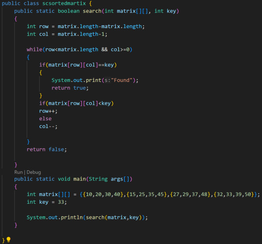
#this was an interesting way to search a element in a sorted 2D array#staircase#javaprogramming#coding#saved
6 notes
·
View notes
Text
Sair’s guide to File Management

also known as ‘there’s that fucker!’
#i organize and explore ideas in 2d arrays#which design software haaates#and this one is getting unwieldy#and about ready to retire
3 notes
·
View notes
Text
My comsci class is online now and Google meet is just as horrifying and scary as I remembered it <3
#i need my teacher to check my code so he can tell me what to do next but i dont wanna let the whole class know 😭#ive left a note in my internal commentary but idk when he'll next check my code#hate it here#my brain has been mush all day so i have no idea how to do what we're doing rn (2d arrays. wtf)#words are going in one ear out the other 😭#psii.txt
5 notes
·
View notes
Text
augh
#ITS SO COOL WHEN THINGS GO THE WAY I WANT!! =w=bb#augh programming can suck but <33#it did the thing i want it to do!!!#YIPPEEE#i made a lil pathway with the cords i provided in a 2d array.#its. not difficult.#but man i'd have no clue about any of this a month ago so <333#heheheheh i love learning#im so glad the internet exists oml i couldnt do it without you!#sillyposting#yay
4 notes
·
View notes
Text
i think i'm too tired to work much on my image viewer build tonight but i'll try in the morning
#have been so slow#thought i'd finish this in 24hrs#need to quickly implement the json formatting/bounding box display and user interactions with file update#and i think that's mostly it? outside of multiple select and maybe some color based speaker display system#then of course need to write the whole ocr backend lol#which is coming out to maybe be training-own-model extent of nightmare#depending on how nicely it plays with furigana#and if it does play nicely with furigana then i need to implement a whole second stage of string analysis#doing some 2d math to combine bounding boxes to display nicely for the viewer i guess#and associating the relevant furiganas#which in json i guess i can just store as an array of kanji char pos len and associated furigana in the recognized line
0 notes
Text
see like i shouldve not procrastinated on finishing this assignment so long but also i literally didnt have time to work on it until today. technically i had yesterday too but i was so dead inside if i actually had to try this i tihnk i wouldve just cried
1 note
·
View note
Text
love finding the right data structure to solve a problem I created. feel like I've mastered engineering or something
#needed a 2d map but c doesnt have hash maps built in#realized i could do it with an array of linked lists#which should have the same if not better amortized/worst case performance due to the structure of the key set#couldnt find a source for how real 3d renderers do what im trying to do#my plan for after graduation honestly might be to keep working on this thing for a while 😂
0 notes
Text
Cars are not the best way to deliver things to you. Radical concept, I know. Even so, our roads are now clogged with a ton of folks just trying to eke out a living by running their personal vehicles into the ground in order to deliver Barbie® clothes, hot dog bun warmers, and last-minute orders of snake penis wine. This constant traffic volume has not gone unnoticed by our plutocratic tormentors: now they must look to the sky to make that quick 5000% margin on a delivery they didn't make.
Drones are the future of last-mile delivery, they tell us. There's a lot more room in the 3D sky than the 2D road, ignoring the fact that a lot of that 3D sky is currently occupied by passenger aircraft that don't want to suck in a buzzing R/C airplane stuffed full of Grandma's prescriptions on its way back from the Kroger-Anne. Those sound like laws, they say, and happily ignore them. The result is that my house is inundated with wasplike shrieking overhead at all hours of the day. Their tiny gerotors and multi-props efficiently slice the wind into the glorious miracle of lift, annoying the shit out of me in the process.
What is an average schlub like myself to do? I'll tell you what the fat cats sending these drones don't want me to do. They don't want me to erect a giant, four-storey-tall net which catches those drones, dropping them helplessly to my lawn where I hit them with a baseball bat until they stop moving. I used to steal the deliveries, too, but you can only drink so much last-minute-ordered snake penis wine before the cops get there. Now I just leave it on the lawn and make it look like an accident.
Of course, the delivery companies are starting to notice a pattern. They probably have hired a particularly bright intern who has plotted all the crashes onto Google Maps, a giant blinking red arrow at my house. That's why I do the catching over my neighbour's house, while he's at work, and also why, in the last couple of weeks, I've been helping myself to more and more of the drone parts.
Sure, there's no law against launching a sixty-ton drone mashed up of thousands of its fallen brethren. There might be a law against flying it slowly over the industrial complex, blotting out the sun on their rooftop solar arrays, and ramming any lesser drone that tries to take off out of the sky, but there probably should be.
697 notes
·
View notes
Text
Researchers Safely Integrate Fragile 2D Materials Into Devices - Technology Org
New Post has been published on https://thedigitalinsider.com/researchers-safely-integrate-fragile-2d-materials-into-devices-technology-org/
Researchers Safely Integrate Fragile 2D Materials Into Devices - Technology Org
The advance opens a path to next-generation devices with unique optical and electronic properties.
Two-dimensional materials, which are only a few atoms thick, can exhibit some incredible properties, such as the ability to carry electric charge extremely efficiently, which could boost the performance of next-generation electronic devices.
This artist’s rendition shows a new integration platform developed by MIT researchers. By engineering surface forces, they can directly integrate 2D materials into devices in a single contact-and-release step. Image credit: Sampson Wilcox/Research Laboratory of Electronics
But integrating 2D materials into devices and systems like computer chips is notoriously difficult. These ultrathin structures can be damaged by conventional fabrication techniques, which often rely on the use of chemicals, high temperatures, or destructive processes like etching.
To overcome this challenge, researchers from MIT and elsewhere have developed a new technique to integrate 2D materials into devices in a single step while keeping the surfaces of the materials and the resulting interfaces pristine and free from defects.
Their method relies on engineering surface forces available at the nanoscale to allow the 2D material to be physically stacked onto other prebuilt device layers. Because the 2D material remains undamaged, the researchers can take full advantage of its unique optical and electrical properties.
They used this approach to fabricate arrays of 2D transistors that achieved new functionalities compared to devices produced using conventional fabrication techniques. Their method, which is versatile enough to be used with many materials, could have diverse applications in high-performance computing, sensing, and flexible electronics.
The developed platform leverages industry-compatible toolsets, allowing for the process to be scaled. Here, lead author Peter Satterthwaite uses a modified alignment tool in MIT.nano to do a patterned, aligned integration. Credits: Courtesy of Weikun Zhu / MIT
Core to unlocking these new functionalities is the ability to form clean interfaces, held together by special forces that exist between all matter, called van der Waals forces.
However, such van der Waals integration of materials into fully functional devices is not always easy, says Farnaz Niroui, assistant professor of electrical engineering and computer science (EECS), a member of the Research Laboratory of Electronics (RLE), and senior author of a new paper describing the work.
“Van der Waals integration has a fundamental limit,” she explains.
“Since these forces depend on the intrinsic properties of the materials, they cannot be readily tuned. As a result, there are some materials that cannot be directly integrated with each other using their van der Waals interactions alone. We have come up with a platform to address this limit to help make van der Waals integration more versatile, to promote the development of 2D-materials-based devices with new and improved functionalities.”
Niroui wrote the paper with lead author Peter Satterthwaite, an electrical engineering and computer science graduate student; Jing Kong, professor of EECS and a member of RLE; and others at MIT, Boston University, National Tsing Hua University in Taiwan, the National Science and Technology Council of Taiwan, and National Cheng Kung University in Taiwan. The research is published today in Nature Electronics.
The diverse surface forces available at the nanoscale enable researchers to adapt the adhesive matrix transfer to many different materials. For example, here, by using adhesive polymers, they are able to transfer patterned graphene, a one-atom-thick sheet of carbon, from a source substrate (top image), to a receiving adhesive polymer (bottom image). Credits: Courtesy of the Niroui Group
Advantageous attraction
Making complex systems such as a computer chip with conventional fabrication techniques can get messy. Typically, a rigid material like silicon is chiseled down to the nanoscale, then interfaced with other components like metal electrodes and insulating layers to form an active device. Such processing can cause damage to the materials.
Recently, researchers have focused on building devices and systems from the bottom up, using 2D materials and a process that requires sequential physical stacking. In this approach, rather than using chemical glues or high temperatures to bond a fragile 2D material to a conventional surface like silicon, researchers leverage van der Waals forces to physically integrate a layer of 2D material onto a device.
Van der Waals forces are natural forces of attraction that exist between all matter. For example, a gecko’s feet can stick to the wall temporarily due to van der Waals forces.
Though all materials exhibit a van der Waals interaction, depending on the material, the forces are not always strong enough to hold them together. For instance, a popular semiconducting 2D material known as molybdenum disulfide will stick to gold, a metal, but won’t directly transfer to insulators like silicon dioxide by just coming into physical contact with that surface.
However, heterostructures made by integrating semiconductor and insulating layers are key building blocks of an electronic device. Previously, this integration has been enabled by bonding the 2D material to an intermediate layer like gold, then using this intermediate layer to transfer the 2D material onto the insulator, before removing the intermediate layer using chemicals or high temperatures.
Instead of using this sacrificial layer, the MIT researchers embed the low-adhesion insulator in a high-adhesion matrix. This adhesive matrix is what makes the 2D material stick to the embedded low-adhesion surface, providing the forces needed to create a van der Waals interface between the 2D material and the insulator.
Making the matrix
To make electronic devices, they form a hybrid surface of metals and insulators on a carrier substrate. This surface is then peeled off and flipped over to reveal a completely smooth top surface that contains the building blocks of the desired device.
This smoothness is important, since gaps between the surface and 2D material can hamper van der Waals interactions. Then, the researchers prepare the 2D material separately, in a completely clean environment, and bring it into direct contact with the prepared device stack.
“Once the hybrid surface is brought into contact with the 2D layer, without needing any high-temperatures, solvents, or sacrificial layers, it can pick up the 2D layer and integrate it with the surface. This way, we are allowing a van der Waals integration that would be traditionally forbidden, but now is possible and allows formation of fully functioning devices in a single step,” Satterthwaite explains.
This single-step process keeps the 2D material interface completely clean, which enables the material to reach its fundamental limits of performance without being held back by defects or contamination.
And because the surfaces also remain pristine, researchers can engineer the surface of the 2D material to form features or connections to other components.
For example, they used this technique to create p-type transistors, which are generally challenging to make with 2D materials. Their transistors have improved on previous studies, and can provide a platform toward studying and achieving the performance needed for practical electronics.
Their approach can be done at scale to make larger arrays of devices. The adhesive matrix technique can also be used with a range of materials, and even with other forces to enhance the versatility of this platform.
For instance, the researchers integrated graphene onto a device, forming the desired van der Waals interfaces using a matrix made with a polymer. In this case, adhesion relies on chemical interactions rather than van der Waals forces alone.
In the future, the researchers want to build on this platform to enable integration of a diverse library of 2D materials to study their intrinsic properties without the influence of processing damage, and develop new device platforms that leverage these superior functionalities.
Written by Adam Zewe
Source: Massachusetts Institute of Technology
You can offer your link to a page which is relevant to the topic of this post.
#2D materials#adhesion#applications#approach#Arrays#atom#atoms#Building#carbon#challenge#chemical#chemicals#Chemistry & materials science news#chips#computer#computer chips#Computer Science#computing#contamination#development#devices#easy#electrodes#electronic#electronic devices#Electronics#Engineer#engineering#Environment#Fabrication
0 notes
Text
been messing around with making a (faked, actually 2D) 3D dungeon crawler without a game engine the last few days - never tried making anything in just C# and monogame with visual studio before, its like a fun puzzle…
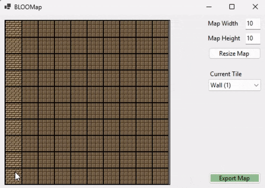
simple little external tool for making the number arrays that generate the maps I put together today, haven't done much like this before either so it's fun, idk how I'd do something like this as simply in unity lol
1K notes
·
View notes
Note
Hey Tracy! Have you heard about the new Ai called Sora? Apparently it can now create 2D and 3D animations as well as hyper realistic videos. I’ve been getting into animation and trying to improve my art for years since I was 7, but now seeing that anyone can create animation/works in just a mare seconds by typing in a couple words, it’s such a huge slap in the face to people who actually put the time and effort into their works and it’s so discouraging! And it has me worried about what’s going to happen next for artists and many others, as-well. There’s already generated voices, generated works stolen from actual artists, generated music, and now this! It’s just so scary that it’s coming this far. 
Yeah, I've seen it. And yeah, it feels like the universe has taken on a 'fuck you in particular' attitude toward artists the past few years. A lot of damage has already been done, and there are plenty of reasons for concern, but bear in mind that we don't know how this will play out yet. Be astute, be justifiably angry, but don't let despair take over. --------
One would expect that the promo clips that have been dropping lately represent some of the best of the best-looking stuff they've been able to produce. And it's only good-looking on an extremely superficial level. It's still riddled with problems if you spend even a moment observing. And I rather suspect, prior to a whole lot of frustrated iteration, most prompts are still going to get you camera-sickness inducing, wibbly-wobbly nonsense with a side of body horror.
Will the tech ultimately get 'smarter' than that and address the array of typical AI giveaways? Maybe. Probably, even. Does that mean it'll be viable in quite the way it's being marketed, more or less as a human-replacer? Well…
A lot of this is hype, and hype is meant to drive up the perceived value of the tech. Executives will rush to be early adopters without a lot of due diligence or forethought because grabbing it first like a dazzled chimp and holding up like a prize ape-rock makes them look like bleeding-edge tech geniuses in their particular ecosystem. They do this because, in turn, that perceived value may make their company profile and valuations go up too, which makes shareholders short-term happy (the only kind of happy they know). The problem is how much actual functional value will it have? And how long does it last? Much of it is the same routine we were seeing with blockchain a few years ago: number go up. Number go up always! Unrealistic, unsustainable forever-growth must be guaranteed in this economic clime. If you can lay off all of your people and replace them with AI, number goes up big and never stops, right?
I have some doubts. ----------------------
The chips also haven't landed yet with regards to the legality of all of this. Will these adopters ultimately be able to copyright any of this output trained on datasets comprised of stolen work? Can computer-made art even be copyrighted at all? How much of a human touch will be required to make something copyright-able? I don't know yet. Neither do the hype team or the early adopters.
Does that mean the tech will be used but will have to be retrained on the adopter's proprietary data? Yeah, maybe. That'd be a somewhat better outcome, at least. It still means human artists make specific things for the machine to learn from. (Watch out for businesses that use 'ethical' as a buzzword to gloss over how many people they've let go from their jobs, though.)
Will it become industry standard practice to do things this way? Maybe. Will it still require an artist's sensbilities and oversignt to plan and curate and fix the results so that it doesn't come across like pure AI trash? Yeah, I think that's pretty likely.
If it becomes standard practice, will it become samey, and self-referential and ultimately an emblem of doing things the cookie-cutter way instead of enlisting real, human artists? Quite possibly.
If it becomes standard industry practice, will there still be an audience or a demand or a desire for art made by human artists? Yes, almost certainly. With every leap of technology, that has remained the case. ------------------ TL;DR Version:
I'm not saying with any certainty that this AI blitz is a passing fad. I think we're likely to experience a torrential amount of generative art, video, voice, music, programming, and text in the coming years, in fact, and it will probably irrevocably change the layout of the career terrain. But I wouldn't be surprised if it was being overhyped as a business strategy right now. And I don't think the immensity of its volume will ever overcome its inherent emptiness.
What I am certain of is that it will not eliminate the innate human impulse to create. Nor the desire to experience art made by a fellow soul. Keep doing your thing, Anon. It's precious. It's authentic. It will be all the more special because it will have come from you, a human.
920 notes
·
View notes
Text
Here’s a personal take!
The Sonic Prime 3D models have the best facial expressions seen from the modern cast. Why? Well, I’ll explain with my 0 experience in 3D animation. I’m only explaining as an observer. Not a professional. Anyways, onto the fun.

First of all, let’s talk about the current models in the games. The animators became better at animating them in Sonic Frontiers.

You can tell effort was being put in, but Frontiers still has limits due to the structure of Sonic’s face and eyes. I’ve seen fan animations with this model which animates him wonderfully. But no matter what, he’s still going to have limitations because his hands are too big, eyes are too far apart, mouth looks like it was made to only stay on the side, and more issues. The design frankly looks dead. Even in motion.


In all fairness, this character was built for a 2D design due to it being inspired by Mickey Mouse. But Sonic Unleashed (because they used different models like Dream Team) proves this character CAN be expressive in 3D with a good workable model. It’s not the animation that’s the problem in Frontiers. Here are similar expressions from Sonic Prime and Frontiers.

See how wider the expressions are in Prime? It allows their faces to be more flexible and warped. Prime!Sonic has rounder eyes making his head look easier for his facial structure to have an array of expressions. It’s kind of close to Sonic Dream Team with the minor tweaks of the OG models. Which is why the expressions in that game looked so good. ESPECIALLY when animated.

It’s even why other designs are able to have great facial expressions. The eyes being close together just works. While the OG looks like he’s pushing expressions that’s near impossible to push. Yes, it’s still expressive, but you can see how limiting it is because the eyes aren’t supporting the face. And his mouth is always stuck to one side.
Onto more compliments to the Sonic Prime models. They emphasize the hight differences too. I personally think Sonic and Shadow look like mixtures between their 06, modern, Boom, and movie designs. They have long quills like 06. Their entire look is inspired by the modern designs. Their eyes are shaped similar to Sonic Boom and they have cool textures like in the movies. Other characters count but it most notably is for the two hedgehogs.

The hands are smaller like in the movies and Boom. The pupils being bigger gives volume to the faces. I also adore their fur and quill patterns to give the designs flare. Their gloves have little details too. I especially love how they can change the quills for Sonic and Shadow and make them look similar to a 2D style. Usually they’d make the quills smaller in the games to get that 2D look but Prime Shadow and Sonic are able to have long quills while the animators adjust them however and whenever they need to.

Their mouths are also well animated and smooth when transitioning to different sides of the face. The characters body shapes are also 100% better. While the Game model looks too straight the Prime model has a pear shape torso that are also given to Boom and Movie Sonic respectively. The Prime models look like they were made for action scenes.

I know some people complain about the eyes not going down, but honestly it’s what makes the expressions weaker when used in 3D. I’m glad they have a balance of it sometimes to allow the expressions to get their points across. I really appreciate the colors on everyone also. They look lovely and bright with help of the lighting.
The few critiques I have are due to multiple watches but they’re not a HUGE deal.
1. I can easily see their necks at points.
2. The mouth animation looks weird when characters makes an O shape and the tongues/teeth are jarring.
3. I wish their hands weren’t so flat and skinny. Other models had their hands shaped like Disney characters, but Prime’s hands can look flat sometimes.
These are just nitpicks though.

Even compared to the CGI cutscenes while still good I think Prime conveys a subtly previous models didn’t do too often. Of course the CGI looks amazing and it still holds up, but the nuance in Sonic Prime cannot be ignored. Hope my take makes the slightest of sense.
Stay Creative! 💜
#sonic prime#sonic the hedgehog#sth#amy rose#amy rose hedgehog#shadow the hedgehog#shadow the ultimate lifeform#miles tails prower#tails the fox#sonic wachowski#movie sonic#sonic movie#Sonic boom#boom!sonic#sonic idw#sonic frontiers#prime!shadow#knuckles the echidna#cream the rabbit#rouge the bat#chip sonic unleashed#Sonic unleashed#shadow games#sonic 06#sonic games#sonic animation#animation#character animation#character design#sonic art
313 notes
·
View notes
Text
This is sort of an indirect addition to this ask maddy got about learning rust, I haven't actually gotten to learning rust yet but I do want to talk about an incident I recently had with python (I think with C the reasons why you'd rather not use it are fairly obvious) So recently tried to implement a basic matrix class in python, and since I wanted to do a whole thing where I did my own implementations of numerical optimization and more general linear algebra stuff, I tried to do it "properly" and make it "robust" and everything, but without installing any external libraries.
And to me, that obviously involved making sure that the matrix is formatted sensibly, i.e. that a matrix contains m rows of n numbers each. This seemed like a very obvious thing you should do in any serious piece of code, since if the contents of a matrix are accidentally formatted in a weird way, then you might get errors, or, significantly worse, python might just decide that it "can handle them" anyways and do some really unintuitive dumb stuff that's really hard to debug. (See this older post of mine for an example of how the pythonic willingness to work with bad inputs leads to really weird unintuitive behavior).
Turns out this is not something you can do directly in python without installing external type checking libraries! And I didn't want to just loop through all the contents and check their type individually during object creation, since that felt incredibly slow, stupid and inefficient. It didnt help that my algorithms theory exam was coming up soon, which meant I was thinking about asymptotic runtimes all day.
And so I was like "well surely at least it's easy to check for a matrix being a 2D array with consistent row sizes". However, at this point, with dawning horror, I came to a realization:

and at this moment I could just feel pretty much all of my remaining "python is easy to work with" attitude turning into dust and soaring away in the wind. If anyone here knows a way to enforce a given argument being a 2D array of numbers with consistent row sizes that doesn't involve O(n*m) overhead during object creation and that can be implemented in python using only internal modules (no external type checkers that need to be installed manually first) please tell me lol
48 notes
·
View notes