#Electronic Design Automation
Explore tagged Tumblr posts
Visit Tumblr Blog
Explore Tumblr blogs with no restrictions, modern design and the best experience.
Last Seen Tumblr Blogs


Fun Fact
Tumblr is available in 18 languages.
Text
PCBs: The Shift from Wire Wrap and Point-to-Point Construction to Automated Manufacturing
Printed Circuit Boards (PCBs) have revolutionized the electronics industry by replacing earlier methods of circuit construction such as wire wrap and point-to-point wiring, both of which were once popular but have now become rarely used due to the growing demand for efficiency, precision, and automation.
Wire Wrap and Point-to-Point Construction: A Historical Overview
In the early days of electronic devices, wire wrap and point-to-point construction were the dominant methods for assembling circuits. Wire wrap involved wrapping a thin wire around a post at each connection point, while point-to-point wiring involved manually connecting components with individual wires. Both methods were labor-intensive and prone to errors, making them less suitable for complex circuits.
While these techniques worked for early applications, they struggled to keep pace with the rapid development of modern electronics, especially as devices grew smaller and more complex. The manual nature of both wire wrap and point-to-point methods meant that they were time-consuming, required skilled labor, and were prone to inconsistency.

The Evolution to PCBs
The advent of PCBs marked a significant departure from these earlier methods. A PCB is a flat board made of non-conductive material, typically fiberglass or composite epoxy, onto which conductive pathways are etched or printed. These pathways, known as traces, connect different electronic components, such as resistors, capacitors, and integrated circuits, without the need for manual wiring.
PCBs offer numerous advantages over wire wrap and point-to-point construction:
Compact Design: PCBs allow for compact and organized circuit layouts, making them ideal for modern electronics where space is a premium.
Reduced Complexity: By eliminating the need for individual wires, PCBs simplify the layout of complex circuits.
Enhanced Durability: The soldered connections on a PCB are more reliable and durable than hand-wrapped or manually connected wires.
Scalability: PCBs are easily scalable for mass production, unlike manual methods that require individual attention to each connection point.
Design Challenges and Automation in PCB Manufacturing
Although PCBs offer many advantages, their design requires careful planning. Unlike wire wrap and point-to-point methods, where connections can be made on-the-fly, PCBs must be carefully designed before they can be manufactured. The layout of a PCB involves placing components and designing the traces that connect them, a process that can be intricate and time-consuming.
To address these challenges, Electronic Design Automation (EDA) software plays a critical role in modern PCB design. EDA tools automate many of the tasks involved in laying out a circuit, including optimizing the placement of components and routing the traces to avoid errors such as short circuits or excessive electromagnetic interference (EMI). These tools not only speed up the design process but also ensure that the resulting board meets the necessary electrical and mechanical requirements.
Automation in PCB Manufacturing and Assembly
Once the design is finalized, PCB manufacturing and assembly can be fully automated. Automated systems can produce large volumes of PCBs with extreme precision, which is essential for industries like consumer electronics, aerospace, and telecommunications.
Manufacturing: Automated machines create PCBs by etching conductive traces onto the board, drilling holes for component leads, and applying solder masks. These processes are highly efficient and scalable for mass production.
Assembly: Surface-mount technology (SMT) and through-hole technology (THT) are commonly used in automated assembly processes. Robotic arms place components onto the board with precision, followed by soldering processes that create strong electrical connections.
Conclusion
While wire wrap and point-to-point construction were once popular techniques for assembling circuits, the advent of PCBs has made these methods largely obsolete. PCBs require additional design effort, but the rewards in terms of automation, reliability, and scalability make them the preferred choice for modern electronics. With the help of electronic design automation software and automated manufacturing processes, PCBs have become the foundation of the modern electronics industry, enabling the rapid production of complex devices with high precision and efficiency.
1 note
·
View note
Text
Exploring Electronic Design Automation (EDA) - ACEIT
Electronic Design Automation (EDA) technologies are critical in the fast-paced field of electronics, where innovation is the key to success and Understanding EDA is essential for students interested in pursuing careers in electrical engineering and industrial automation also we will dissect the complexity of Electronic Design Automation, investigating its relevance, applicability, and critical position in the specialized subject of Industrial Automation within Electrical Engineering schools.
What Is Electronic Design Automation (EDA)?
Electronic Design Automation refers to a category of software tools used for designing electronic systems such as integrated circuits and printed circuit boards. EDA tools facilitate the design, analysis, and simulation of electronic systems, ensuring efficiency and accuracy in the development process.
Significance Of EDA In Electrical Engineering
Streamlining the Design Process:
EDA tools streamline the design process by providing a virtual platform where engineers can create, test, and modify their designs This iterative process enhances creativity and innovation.
Cost Efficiency:
By identifying errors and optimizing designs before physical prototypes are created, EDA tools significantly reduce development costs, also this cost efficiency is paramount, especially in large-scale industrial projects.
Simulation and Analysis:
EDA tools enable engineers to simulate and analyze the behavior of electronic circuits under different conditions as well as this virtual testing ensures that the final product meets the required specifications and standards.
Time-Saving:
In the competitive world of technology, time-to-market is crucial. EDA tools accelerate the design process, allowing engineers to meet tight deadlines without compromising on quality.
Applications Of EDA:
Integrated Circuit (IC) Design:
EDA tools are extensively used in IC design, enabling engineers to create complex circuits with millions of transistors However, these circuits power various electronic devices, from smartphones to computers.
Printed Circuit Board (PCB) Design:
In PCB design, EDA tools assist engineers in creating the layout of electronic components on a board, So this layout is fundamental for the proper functioning of devices like laptops, televisions, and medical equipment.
FPGA (Field-Programmable Gate Array) Design:
FPGAs are versatile chips that can be programmed to perform specific tasks also EDA tools aid engineers in designing and programming FPGAs for applications in telecommunications, automotive, and aerospace industries.
1 note
·
View note
Text

#robot#robotics#robots#technology#art#engineering#arduino#d#electronics#transformers#mecha#tech#toys#anime#robotic#scifi#gundam#ai#drawing#artificialintelligence#digitalart#innovation#illustration#electrical#automation#robotica#diy#design#arduinoproject#iot
33 notes
·
View notes
Text
North America Electronic Design Automation Market Analysis by Business Methodologies 2027
North America Electronic Design Automation Market is expected to grow from US$ 4.10 Bn in 2018 to US$ 9.70 Bn by the year 2027 with a CAGR of 10.2% from the year 2019 to 2027.
Market Overview
The significant growth impetus emanating from the semiconductor industry is a primary driver fueling the substantial expansion of the North America Electronic Design Automation Market. Furthermore, the increasing focus on the reduction in size of electronic devices is widely anticipated to stimulate the progress of the North America Electronic Design Automation Market throughout the forecast period. Moreover, the growing number of significant collaborations and strategic partnerships among key players within the electronic design automation (EDA) sector is a crucial factor fostering market expansion. The North America Electronic Design Automation Market is characterized by the strong presence of numerous well-established global companies, alongside a considerable number of smaller, tier-two enterprises. These EDA companies are playing a vital role in enabling semiconductor manufacturers to effectively meet the continuously increasing demand for sophisticated semiconductor products from their diverse customer base within the North America Electronic Design Automation Market.
Request sample PDF:
https://www.businessmarketinsights.com/sample/TIPRE00005732
In the year 2018, the Semiconductor Intellectual Property (SIP) segment held a dominant position within the Electronic Design Automation market, commanding the largest share of the market. However, industry forecasts indicate an anticipated shift in dominance, with the Computer-Aided Engineering (CAE) segment projected to surpass SIP over the forecast period within the North America Electronic Design Automation Market. Semiconductor IP is fundamental to the creation of large-scale and highly intricate Integrated Circuits (ICs), which are essential building blocks in a vast array of electronic devices. Notably, the automotive industry has experienced a remarkable surge in its demand for semiconductors, fueled by the continuous advancements in automotive electronics, including sophisticated driver-assistance systems and advanced infotainment platforms, impacting the North America Electronic Design Automation Market. Furthermore, the IT & Telecommunications sector has witnessed a dynamic and sustained increase in the demand for semiconductors, particularly for processor IP, which, in turn, is prompting memory semiconductor IP manufacturers to actively invest in expanding their production capacities to cater to the growing needs of the North America Electronic Design Automation Market. This proactive investment is projected to contribute to a favorable outlook for the semiconductor IP market throughout the forecast period. The escalating demand for advanced System-on-Chip (SoC) designs has significantly propelled the growth of this market segment within the North America Electronic Design Automation Market. Further contributing to this trend is the increasing adoption of consumer electronics within the North America region, which is specifically driving the greater utilization of semiconductor IP.
The United States held a leading position in the electronic design automation market in 2018 and is projected to maintain its dominance within the market across the North American region throughout the forecast period. The semiconductor industry has consistently been a critical pillar of national security, economic prosperity, and global technological leadership for North America. The US, within the context of the semiconductor industry, is not only the foremost economy in North America but also a substantial contributor to the global market. Furthermore, as a technologically advanced nation, the adoption and implementation of EDA software are anticipated to remain at a high level within the North America Electronic Design Automation Market. However, it is anticipated that the North America Electronic Design Automation Market may gradually approach a state of maturity in the coming years, primarily due to the projected moderation in the growth rate of the semiconductor industry. Nevertheless, ongoing innovation and the persistent demand for advanced electronic products will ensure the continued significance and dynamism of the North America Electronic Design Automation Market.
About Us:
Business Market Insights is a market research platform that provides subscription service for industry and company reports. Our research team has extensive professional expertise in domains such as Electronics & Semiconductor; Aerospace & Defense; Automotive & Transportation; Energy & Power; Healthcare; Manufacturing & Construction; Food & Beverages; Chemicals & Materials; and Technology, Media, & Telecommunications
#North America Electronic Design Automation Market#North America Electronic Design Automation Market Segmentation#North America Electronic Design Automation Market Overview
0 notes
Text
Beats, Bytes & The Future Sound: AI Meets Electronic Music
Electronic music has always been about pushing boundaries, breaking rules, and bending sound into new dimensions. Now, artificial intelligence is stepping into the booth, reshaping how beats are built, melodies emerge, and tracks come to life. This isn’t about robots replacing producers—it’s about a new creative partnership, where human intuition meets machine-driven possibilities.The Evolution…
#AI and sound design#AI beat generation#AI for producers#AI in electronic music#AI in music production#AI mixing and mastering#AI music algorithms#AI music collaboration#AI music creation#AI music technology#AI music trends.#AI rhythm generation#AI-driven sound synthesis#AI-generated beats#AI-powered music software#artificial intelligence in techno#artificial intelligence music production#automated music production#creative AI music#digital music production#electronic music and AI#electronic music tools#future of music production#machine learning music#music composition AI#music innovation AI#music production AI tools#music production tools#neural networks in music#sound design AI
0 notes
Text
UK must act to secure its semiconductor industry leadership
New Post has been published on https://thedigitalinsider.com/uk-must-act-to-secure-its-semiconductor-industry-leadership/
UK must act to secure its semiconductor industry leadership
The UK semiconductor industry is at a critical juncture, with techUK urging the government to act to maintain its global competitiveness.
Laura Foster, Associate Director of Technology and Innovation at techUK, said: “The UK has a unique opportunity to lead in the global semiconductor landscape, but success will require bold action and sustained commitment.
“By accelerating the implementation of the National Semiconductor Strategy, we can unlock investment, foster innovation, and strengthen our position in this critical industry.
Semiconductors are the backbone of modern technology, powering everything from consumer electronics to AI data centres. With the global semiconductor market projected to reach $1 trillion by 2030, the UK must act to secure its historic leadership in this lucrative and strategically vital industry.
“We must act at pace to secure the UK’s semiconductor future and as such our technological and economic resilience,” explains Foster.
UK semiconductor industry strengths and challenges
The UK has long been a leader in semiconductor design and intellectual property (IP), with Cambridge in particular serving as a global hub for innovation.
Companies like Arm, which designs chips used in 99% of the world’s smartphones, exemplify the UK’s strengths in this area. However, a techUK report warns that these strengths are under threat due to insufficient investment, skills shortages, and a lack of tailored support for the sector.
“The UK is not starting from zero,” the report states. “We have globally competitive capabilities in design and IP, but we must double down on these strengths to compete internationally.”
The UK’s semiconductor industry contributed £12 billion in turnover in 2021, with 90% of companies expecting growth in the coming years. However, the sector faces significant challenges, including high costs, limited access to private capital, and a reliance on international talent.
The report highlights that only 5% of funding for UK semiconductor startups originates domestically, with many companies struggling to find qualified investors.
A fundamental need for strategic investment and innovation
The report makes 27 recommendations across six key areas, including design and IP, R&D, manufacturing, skills, and global partnerships.
Some of the key proposals include:
Turn current strengths into leadership: The UK must leverage its existing capabilities in design, IP, and compound semiconductors. This includes supporting regional clusters like Cambridge and South Wales, which have proven track records of innovation.
Establishing a National Semiconductor Centre: This would act as a central hub for the industry, providing support for businesses, coordinating R&D efforts, and fostering collaboration between academia and industry.
Expanding R&D tax credits: The report calls for the inclusion of capital expenditure in R&D tax credits to incentivise investment in new facilities and equipment.
Creating a Design Competence Centre: This would provide shared facilities for chip designers, reducing the financial risk of innovation and supporting the development of advanced designs.
Nurturing skills: The UK must address the skills shortage in the semiconductor sector by upskilling workers, attracting international talent, and promoting STEM education.
Capitalise on global partnerships: The UK must strengthen its position in the global semiconductor supply chain by forming strategic partnerships with allied countries. This includes collaborating on R&D, securing access to critical materials, and navigating export controls.
Urgent action is required to secure the UK semiconductor industry
The report warns that the UK risks falling behind other nations if it does not act quickly. Countries like the US, China, and the EU have already announced significant investments in their domestic semiconductor industries.
The European Chips Act, for example, has committed €43 billion to support semiconductor infrastructure, skills, and startups.
“Governments across the world are acting quickly to attract semiconductor companies while also building domestic capability,” the report states. “The UK must use its existing resources tactically, playing to its globally recognised strengths within the semiconductor value chain.”
The UK’s semiconductor industry has the potential to be a global leader, but this will require sustained investment, strategic planning, and collaboration between government, industry, and academia.
“The UK Government should look to its semiconductor ambitions as an essential part of delivering the wider Industrial Strategy and securing not just the fastest growth in the G7, but also secure and resilient economic growth,” the report concludes.
(Photo by Rocco Dipoppa)
See also: AI in 2025: Purpose-driven models, human integration, and more
Want to learn more about AI and big data from industry leaders? Check out AI & Big Data Expo taking place in Amsterdam, California, and London. The comprehensive event is co-located with other leading events including Intelligent Automation Conference, BlockX, Digital Transformation Week, and Cyber Security & Cloud Expo.
Explore other upcoming enterprise technology events and webinars powered by TechForge here.
#2025#academia#ai#ai & big data expo#amp#arm#Artificial Intelligence#automation#Big Data#billion#Building#california#China#chip#chips#chips act#Cloud#clusters#Collaboration#Companies#comprehensive#conference#consumer electronics#cyber#cyber security#data#Data Center#data centres#Design#designers
1 note
·
View note
Text
Electronic Design Automation Software Market Size And Share Report, 2030
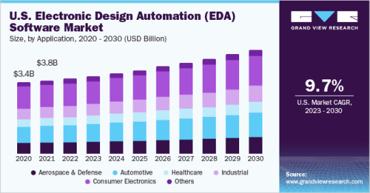
Electronic Design Automation Software Market Growth & Trends
The global electronic design automation software market size is anticipated to reach USD 22.21 billion by 2030, expanding at a CAGR of 9.1% from 2023 to 2030, according to a new study by Grand View Research Inc. The growing usage of advanced electronic components across different areas of healthcare, automotive, and consumer electronic sectors is driving Electronic Design Automation (EDA) software market growth. Apart from this, the proliferation of the Internet of Things (IoT) and connected devices further promotes EDA software market advancement.
Miniaturization of devices and chips is expected to create lucrative opportunities for EDA software. This software assists chipmakers in lowering the errors in Integrated Circuit (IC) and chips, thereby driving the electronic design automation software industry growth. The exponential growth of the integrated circuits market is driving the need for electronic design automation software. The software is increasingly being adopted for designing electronic systems such as printed circuit boards and integrated circuits, supporting the growth of the EDA market.
Furthermore, developments in technology, growing digitization, growth of the electronics manufacturing industry, and increasing adoption of advanced rendering & simulation tools by hardware designers are expected to positively influence the electronic design automation software industry growth over the forecast period. Furthermore, the increasing acceptance and awareness of smart fitness devices are factors enabling electronic design companies to invest in innovative design software tools for designing enhanced & compact products, thereby propelling the EDA software market growth over the forecast period.
Growing demand for EDA software is encouraging various market players to adopt various business strategies to achieve higher profitability in the market for electronic design automation software. Market players are unveiling new solutions by partnering with technology providers to improve their brand identity, propelling the EDA software market growth. For instance, in January 2022, Altium LLC announced a partnership with MacroFab, Inc., a U.S.-based cloud platform provider for electronic production, to launch “Altimade.” The new solution combines elastic manufacturing capabilities and real-time supply chain data, available on the Altium 365 electronic design platform. Altimade empowers customers to request instant quotes and place orders for manufacturing their PCB assembly without exiting the design environment.
Request a free sample copy or view report summary: https://www.grandviewresearch.com/industry-analysis/electronic-design-automation-eda-software-market
Electronic Design Automation Software Market Report Highlights
The services segment is expected to register a CAGR of 10.6% from 2023 to 2030. The segment growth can be attributed to the increasing proclivity of OEMs to outsource their design needs. Furthermore, electronic circuit boards are in high demand in the industry due to their increasing importance in a variety of vital electronic products such as mobile phones and tablets
The cloud segment is expected to register a CAGR of 10.8% from 2023 to 2030. Cloud-based deployment allows for faster distribution, less maintenance, lower costs, and more scalability
The healthcare segment is expected to register a CAGR of 11.5% from 2023 to 2030. The segment growth can be attributed to the benefits of EDA software in healthcare, such as lower costs, improved patient outcomes, faster design & development, enabled regulatory compliance of medical devices, and simulation and testing of medical equipment
The microprocessors & controllers segment is expected to register a CAGR of 9.5% from 2023 to 2030. The increased use of microprocessors in consumer devices such as smartphones, personal computers (PCs), and laptops is expected to drive global demand for the segment
Asia Pacific is anticipated to emerge as the fastest-growing region over the forecast period at a CAGR of 9.6%. A surge in demand for electronic devices together with the prevalence of key electronic component manufacturers in Greater China is expected to drive regional growth
Electronic Design Automation Software Market Segmentation
Grand View Research has segmented the global electronic design automation software market based on product, deployment, application, end-use, and region:
Electronic Design Automation (EDA) Software Product Outlook (Revenue, USD Billion, 2018 - 2030)
Computer-aided Engineering (CAE)
IC Physical Design and Verification
Printed Circuit Board and Multi-chip Module (PCB and MCM)
Semiconductor Intellectual Property (SIP)
Services
Electronic Design Automation (EDA) Software Deployment Outlook (Revenue, USD Billion, 2018 - 2030)
Cloud
On-premise
Electronic Design Automation (EDA) Software Application Outlook (Revenue, USD Billion, 2018 - 2030)
Aerospace and Defense
Automotive
Healthcare
Industrial
Consumer Electronics
Others
Electronic Design Automation (EDA) Software End-use Outlook (Revenue, USD Billion, 2018 - 2030)
Microprocessors & Controllers
Memory Management Unit (MMU)
Others
Electronic Design Automation (EDA) Software Regional Outlook (Revenue, USD Billion, 2018 - 2030)
North America
Europe
Asia Pacific
Latin America
Middle East & Africa
List of Key Players in the Electronic Design Automation Software Market
Advanced Micro Devices, Inc.
Aldec, Inc.
Altair Engineering Inc.
Altium LLC
Autodesk, Inc.
ANSYS, Inc.
Cadence Design Systems, Inc.
eInfochips
EMA Design Automation, Inc.
Keysight Technologies
Microsemi
Synopsys, Inc.
Silvaco, Inc.
The MathWorks, Inc.
Vennsa Technologies
Zuken
Browse Full Report: https://www.grandviewresearch.com/industry-analysis/electronic-design-automation-eda-software-market
#Electronic Design Automation Software Market#Electronic Design Automation Software Market Size#Electronic Design Automation Software Market Share
0 notes
Text
What Makes Aimtron Electronics a Leader in ESDM and PCB Assembly?

In today’s fast-paced world of electronics manufacturing, companies are constantly looking for ways to innovate, streamline operations, and improve the quality of their products. One company that stands out in this space is Aimtron Electronics, a leader in the field of Electronics System Design and Manufacturing (ESDM) and PCB (Printed Circuit Board) Assembly. But what sets AImtron apart from its competitors?
Let’s explore the key factors that have helped Aimtron Electronics become a trailblazer in the ESDM and PCB assembly industries.
1. Comprehensive End-to-End ESDM Solutions
Aimtron Electronics offers a complete range of services that span the entire product lifecycle, from initial concept to final delivery. This end-to-end capability allows the company to provide tailored solutions that meet the unique needs of its clients. Whether it's designing a custom PCB, developing complex electronics systems, or providing full-scale manufacturing, Aimtron integrates each step seamlessly, ensuring quality and efficiency throughout the process.
This ability to handle every phase of the development cycle means clients don't have to manage multiple vendors, which can lead to miscommunication, delays, and inconsistencies. Aimtron’s holistic approach not only simplifies the process but also accelerates time-to-market, which is crucial in today’s competitive electronics landscape.
2. Cutting-Edge PCB Assembly Technology
Aimtron Electronics has built a reputation for using the latest technology and techniques in PCB assembly. The company invests heavily in advanced manufacturing equipment, including pick-and-place machines, automated optical inspection (AOI) systems, and reflow soldering technology. These innovations ensure that each PCB assembly is completed with the highest level of precision and reliability.
Moreover, Aimtron’s facilities are designed to handle a wide range of PCB assembly types, including single-sided, double-sided, and multi-layer boards. This versatility means that the company can meet the needs of a variety of industries, from consumer electronics to automotive and industrial applications.
3. Uncompromising Quality Control Standards
One of the hallmarks of AImtron Electronics is its commitment to quality. The company adheres to strict industry standards, such as ISO 9001 and IPC-2221, ensuring that its products meet or exceed the highest benchmarks in the ESDM and PCB assembly industries. AImtron integrates quality control (QC) at every stage of the production process, from design to final assembly.
To further ensure the reliability of its products, AImtron employs automated testing systems, in-circuit testing (ICT), and functional testing to detect any potential defects early in the process. These rigorous quality control measures reduce the likelihood of failure and improve the overall performance of the final product.
4. Design Expertise and Innovation
At Aimtron, the design team is at the heart of everything. The company’s engineers are experts in Electronics System Design (ESD), with deep knowledge in a wide variety of industries and applications. AImtron’s design capabilities cover a broad spectrum, including analog circuits, digital circuits, RF (Radio Frequency) designs, and power electronics.
The team works closely with clients to understand their unique needs and provide innovative solutions that align with their business goals. This collaborative approach ensures that each design is optimized for performance, manufacturability, and cost-efficiency. Additionally, Aimtron’s design team uses state-of-the-art CAD (Computer-Aided Design) software to create accurate and detailed schematics, reducing the likelihood of errors and streamlining the design-to-manufacturing transition.
5. Scalability and Flexibility
Aimtron Electronics excels in delivering scalable solutions. Whether a customer needs a small batch run for prototyping or high-volume production for large-scale manufacturing, Aimtron has the capacity and flexibility to meet diverse demands. The company’s manufacturing facilities are designed for scalability, enabling it to accommodate both small and large orders with equal efficiency and quality.
This flexibility is particularly beneficial for clients in industries such as medical devices, telecommunications, automotive, and aerospace, where demands can fluctuate based on market conditions, regulations, and technological advancements.
6. Commitment to Sustainability
As industries increasingly focus on reducing their environmental footprint, Aimtron Electronics has taken significant steps to ensure that its operations are both efficient and eco-friendly. The company actively embraces green manufacturing practices, such as reducing waste, recycling materials, and utilizing energy-efficient technologies in its PCB assembly process.
Aimtron also works with clients to develop environmentally friendly products, ensuring that their designs are not only high-performing but also sustainable. This commitment to sustainability resonates with clients who are looking to reduce their carbon footprint and meet global environmental standards.
7. Customer-Centric Approach
Aimtron’s customer-centric approach is one of the key factors that sets it apart from other companies in the ESDM and PCB assembly space. From the initial consultation to after-sales support, Aimtron places a strong emphasis on building lasting relationships with its clients.
The company offers personalized service, ensuring that each customer’s unique needs are met with tailored solutions. Aimtron’s engineering team works hand-in-hand with clients to refine designs, troubleshoot issues, and optimize product performance. Additionally, the company’s customer service team is always available to provide ongoing support, from product updates to maintenance and repair services.
8. Global Reach with Local Expertise
While Aimtron Electronics operates on a global scale, it combines this reach with local expertise to serve a diverse client base across multiple industries. The company’s team understands the nuances of different markets, from regional regulations and certifications to cultural considerations in manufacturing.
Aimtron’s ability to navigate these complexities while delivering top-tier ESDM and PCB assembly services has earned the company a strong reputation as a trusted partner in the global electronics supply chain.
Conclusion
Aimtron Electronics stands out as a leader in Electronics System Design and Manufacturing (ESDM) and PCB Assembly due to its combination of cutting-edge technology, rigorous quality standards, innovative design expertise, and a customer-focused approach. The company’s commitment to excellence, scalability, and sustainability has positioned it as a trusted partner for companies across a variety of industries.
With a strong emphasis on precision, efficiency, and reliability, Aimtron Electronics continues to push the boundaries of what’s possible in electronics manufacturing, ensuring that its clients remain competitive in an ever-evolving market.
If you're looking for a partner who can handle all your ESDM and PCB assembly needs, Amitron Electronics offers the experience, technology, and customer care you need to succeed.
#Electronics System Design and Manufacturing (ESDM)#PCB Assembly#Electronics System Design#functional testing#automated optical inspection#reflow soldering#ESDM Solutions
0 notes
Text
SwitchBot Electronic Blinds: A Smart Home Revolution
Has anyone tried the SwitchBot electronic blinds? I would love to hear your thoughts and reviews! They seem like a fantastic addition to any smart home, making it so easy to control natural light with just a tap on your smartphone. If you're looking to upgrade your space, these blinds might be the perfect solution. Imagine the convenience of adjusting your blinds without leaving your couch or getting out of bed!
#SwitchBot#electronic blinds#smart home#natural light#smartphone control#home automation#convenience#upgrade#interior design
0 notes
Text
#career opportunities in EEE#Electrical and Electronics Engineering#EEE careers#MKCE#M.Kumarasamy College of Engineering#power generation and distribution#electronics design and manufacturing#telecommunications careers#AI in electrical engineering#machine learning in EEE#automation and control systems#research and development in EEE#higher education in EEE#teaching careers in EEE#electric vehicles careers#renewable energy careers
0 notes
Text
Cost-Effective Strategies for Efficient PCB Production by A-Gas Electronic Materials
Learn how to optimise PCB production with cost-effective strategies, including design for manufacturability, efficient production techniques, and energy efficiency. Improve quality and reduce costs. Contact A-Gas Electronic Materials for expert guidance and tailored solutions.
#PCB production#cost-effective PCB manufacturing#design for manufacturability#PCB materials#efficient PCB production#supplier collaboration#PCB inventory management#PCB energy efficiency#automated assembly#A-Gas Electronic Materials#UK#PCB production strategies#PCB quality improvement
0 notes
Text
Beats, Bytes & The Future Sound: AI Meets Electronic Music
Electronic music has always been about pushing boundaries, breaking rules, and bending sound into new dimensions. Now, artificial intelligence is stepping into the booth, reshaping how beats are built, melodies emerge, and tracks come to life. This isn’t about robots replacing producers—it’s about a new creative partnership, where human intuition meets machine-driven possibilities.The Evolution…
#AI and sound design#AI beat generation#AI for producers#AI in electronic music#AI in music production#AI mixing and mastering#AI music algorithms#AI music collaboration#AI music creation#AI music technology#AI music trends.#AI rhythm generation#AI-driven sound synthesis#AI-generated beats#AI-powered music software#artificial intelligence in techno#artificial intelligence music production#automated music production#creative AI music#digital music production#electronic music and AI#electronic music tools#future of music production#machine learning music#music composition AI#music innovation AI#music production AI tools#music production tools#neural networks in music#sound design AI
0 notes
Text
3D-ViTac: Low-Cost Tactile Sensing System Bridges Human-Robot Gap
New Post has been published on https://thedigitalinsider.com/3d-vitac-low-cost-tactile-sensing-system-bridges-human-robot-gap/
3D-ViTac: Low-Cost Tactile Sensing System Bridges Human-Robot Gap
The world of robotics faces a persistent challenge: replicating the intricate sensory capabilities that humans naturally possess. While robots have made remarkable strides in visual processing, they’ve historically struggled to match the nuanced touch sensitivity that allows humans to handle everything from fragile eggs to complex tools with ease.
A team of researchers from Columbia University, University of Illinois Urbana-Champaign, and University of Washington has developed an innovative solution called 3D-ViTac, a multi-modal sensing and learning system that brings robots closer to human-like dexterity. This innovative system combines visual perception with sophisticated touch sensing, enabling robots to perform precise manipulations that were previously considered too complex or risky.
Hardware Design
The 3D-ViTac system represents a significant breakthrough in accessibility, with each sensor pad and reading board costing approximately $20. This dramatic reduction in cost, compared to traditional tactile sensors that can run into thousands of dollars, makes advanced robotic manipulation more accessible for research and practical applications.
The system features a dense array of tactile sensors, with each finger equipped with a 16×16 sensor grid. These sensors provide detailed feedback about physical contact, measuring both the presence and force of touch across an area as small as 3 square millimeters. This high-resolution sensing enables robots to detect subtle changes in pressure and contact patterns, crucial for handling delicate objects.
One of the most innovative aspects of 3D-ViTac is its integration with soft robotic grippers. The team developed flexible sensor pads that seamlessly bond with soft, adaptable grippers. This combination provides two key advantages: the soft material increases the contact area between sensors and objects, while also adding mechanical compliance that helps prevent damage to fragile items.
The system’s architecture includes a custom-designed readout circuit that processes tactile signals at approximately 32 frames per second, providing real-time feedback that allows robots to adjust their grip strength and position dynamically. This rapid processing is crucial for maintaining stable control during complex manipulation tasks.
Enhanced Manipulation Capabilities
The 3D-ViTac system demonstrates remarkable versatility across a range of complex tasks that have traditionally challenged robotic systems. Through extensive testing, the system successfully handled tasks requiring both precision and adaptability, from manipulating fragile objects to performing intricate tool-based operations.
Key achievements include:
Delicate object handling: Successfully grasping and transporting eggs and grapes without damage
Complex tool manipulation: Precise control of utensils and mechanical tools
Bimanual coordination: Synchronized two-handed operations like opening containers and transferring objects
In-hand adjustments: Ability to reposition objects while maintaining stable control
One of the most significant advances demonstrated by 3D-ViTac is its ability to maintain effective control even when visual information is limited or blocked. The system’s tactile feedback provides crucial information about object position and contact forces, allowing robots to operate effectively even when they can’t fully see what they’re manipulating.
Technical Innovation
The system’s most groundbreaking technical achievement is its successful integration of visual and tactile data into a unified 3D representation. This approach mirrors human sensory processing, where visual and touch information work together seamlessly to guide movements and adjustments.
The technical architecture includes:
Multi-modal data fusion combining visual point clouds with tactile information
Real-time processing of sensor data at 32Hz
Integration with diffusion policies for improved learning capabilities
Adaptive feedback systems for force control
The system employs sophisticated imitation learning techniques, allowing robots to learn from human demonstrations. This approach enables the system to:
Capture and replicate complex manipulation strategies
Adapt learned behaviors to varying conditions
Improve performance through continued practice
Generate appropriate responses to unexpected situations
The combination of advanced hardware and sophisticated learning algorithms creates a system that can effectively translate human-demonstrated skills into robust robotic capabilities. This represents a significant step forward in creating more adaptable and capable robotic systems.
Future Implications and Applications
The development of 3D-ViTac opens new possibilities for automated manufacturing and assembly processes. The system’s ability to handle delicate components with precision, combined with its affordable price point, makes it particularly attractive for industries where traditional automation has been challenging to implement.
Potential applications include:
Electronics assembly
Food handling and packaging
Medical supply management
Quality control inspection
Precision parts assembly
The system’s sophisticated touch sensitivity and precise control capabilities make it particularly promising for healthcare applications. From handling medical instruments to assisting in patient care, the technology could enable more sophisticated robotic assistance in medical settings.
The open nature of the system’s design and its low cost could accelerate robotics research across academic and industrial settings. The researchers have committed to releasing comprehensive tutorials for hardware manufacturing, potentially spurring further innovations in the field.
A New Chapter in Robotics
The development of 3D-ViTac represents more than just a technical achievement; it marks a fundamental shift in how robots can interact with their environment. By combining affordable hardware with sophisticated software integration, the system brings us closer to robots that can match human dexterity and adaptability.
The implications of this breakthrough extend beyond the laboratory. As the technology matures, we could see robots taking on increasingly complex tasks in various settings, from manufacturing floors to medical facilities. The system’s ability to handle delicate objects with precision while maintaining cost-effectiveness could democratize access to advanced robotics technology.
While the current system demonstrates impressive capabilities, the research team acknowledges areas for future development. Potential improvements include enhanced simulation capabilities for faster learning and broader application scenarios. As the technology continues to evolve, we may see even more sophisticated applications of this groundbreaking approach to robotic manipulation.
#3d#Accessibility#Algorithms#applications#approach#architecture#automation#board#Capture#challenge#clouds#compliance#comprehensive#Containers#data#Design#development#diffusion#Electronics#Environment#Facilities#Features#Fundamental#Fusion#Future#gap#grid#hand#Hardware#healthcare
0 notes
Text

Discover how SIENNA ECAD is transforming the PCB design landscape through innovative Electronic Design Automation solutions. Their expertise in complex layouts and advanced analysis techniques is driving the future of electronics, offering custom solutions across industries. Learn more about their journey and the cutting-edge services they provide at Avalon Technologies. Dive into the full story here.
#pcbdesign hashtag#electronic hashtag#design hashtag#automation hashtag#innovationinelectronics hashtag#eda hashtag#electronicsmanufacturing hashtag#techinnovation hashtag#engineeringexcellence Avalon Technologies Limited Sienna Corporation Sienna ECAD Technologies Private Limited
0 notes