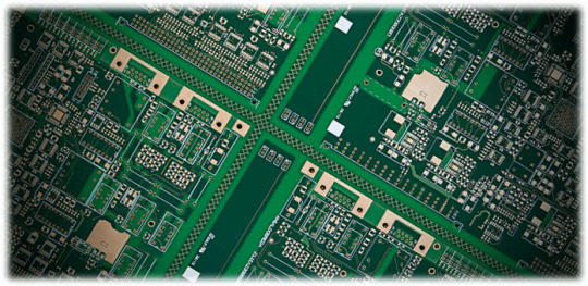
#PCB Evolution
Explore tagged Tumblr posts
Visit Tumblr Blog
Explore Tumblr blogs with no restrictions, modern design and the best experience.
Last Seen Tumblr Blogs


Fun Fact
China blocked Tumblr because of pornography and censorship problems in 2013.
Text
Explore the transformative impact of Advanced PCB Technology on modern electronics with A-Gas Electronic Materials. Dive into the evolution, significance, and future of PCBs in our latest article. Discover how PCBs are reshaping industries from consumer electronics to healthcare. Join the revolution and partner with A-Gas for cutting-edge electronic solutions. Read more now!
#Advanced PCB Technology#Modern Electronics#A-Gas Electronic Materials#Printed Circuit Boards#Electronic Components#PCB Evolution
0 notes
Text

Ever wonder about those little boards inside all our gadgets? They're called printed circuit boards, or PCBs. These unsung heroes started out pretty humble in the early 1900s, just barebones components for radios. Fast forward to today and PCBs are the foundation of nearly every device we use. Read all about the evolution and exciting future of PCBs!
0 notes
Text
touhou 19 time! this game was literally not even released when i started this, so this is really fresh! this post is probably the closest i will ever be to a real games journalist lol.
nina's thoughts on Touhou 19 - Unfinished Dream of All Living Ghost
the most recent touhou, coming out just a few weeks ago, so this review is hot off the presses! UDoALG (wild abbreviation by the way, this name is so long) is a pretty neat game, being a direct sequel to Wily Beast and Weakest Creature story-wise, and a sequel to Phantasmagoria of Flower View gameplay-wise.
UDoALG is another in the competitive-danmaku type gameplay, similar to PoFV but with a number of evolutions to make the gameplay more balanced and easier to control. i won't go over every little change, since theres quite a lot, but ill point out some interesting changes, mostly in relation to story mode. for starters, Ability Cards are back again from UM, although with a much smaller role. each character has 2 cards themed to them, and whenever you beat an opponent in story mode you're randomly given one of their two cards. the three animal spirits are added, but they work completely differently to WBaWC, now being stronger variants of the generic spirit enemies from PoFV. a change that i think is only in story mode is that a new win condition is added, where if you defeat your opponent's boss summon an amount of times then your opponent loses. this is also pretty much the only wincon in story mode, since the AI has insane dodging skills. i literally only saw them lose a life one (1) time across 19 characters' stories (if you're curious, it was in Chiyari's stage 1).
one really interesting aspect of this game is the storytelling. i usually don't bring up the story in these posts outside of how certain characters relate to it, the story usually is a fairly simple affair that just gives the characters a reason to fight, but UDoALG has a much more complex story, which im kinda mixed on. i'll start with the cool part: the story actually progresses as you play through and unlock various characters in story mode, every set of character unlocks represents a later time period of the story, so you don't get the full story and resolution until you play through it all. this is a super cool idea, and gives good incentive to keep playing different routes and see how it all plays out. its a cool idea that uniquely plays off of the large character roster and unlocking method of these competitive vs games.
unfortunately, in order to make this happen and make every character be relevant, the plot is needlessly convuluted, especially in the first couple campaigns. there are so many factions at play, all with their own motives and double-agents and subterfuge. by the end of the 19 story scenarios you will be absolutely sick of the phrase "this is exactly as i had planned", and yet i still dont fully understand What the "main villain"s plan was. i commend ZUN for trying something new with the narrative, both in doing a direct sequel with most of the same characters as a former game, as well as this way of unfolding the story over time through different character routes, but i can't say it was Good. maybe im just biased since it mostly revolves around the WBaWC cast, and that game already had pretty rough plot and characterization, but i dunno. i will say i liked the story more at the end than i did after doing the first couple routes, but some of that early confusion never really goes away, and characters like Ran and Tsukasa dont really get their stories resolved.
time to talk about the characters! UDoALG is furry city, pretty much every character besides the human incident resolvers is some kind of animal-person, plus a few Onis. for returning characters we have Reimu, Marisa, Sanae, Ran (from PCB), Aunn (HSiFS), Nazrin (UFO), Seiran (LoLK), Rin (SA), Tsukasa (UM), Mamizou (TD), Yachie (WBaWC), Saki (WBaWC), Yuuma (the 3rd Animal Realm leader, coming from a fighting game i think?), and Suika (also a fighting game, and SA). for the new characters, we have 3 new youkai who have each joined one of the animal realm families respectively, plus the 'main villain' Zanmu and her assistant Hisami. since theres only 5 new guys, ill just give them each a quick review.
Son Biten is a monkey youkai, based on Son Wukong, recruited to Yachie's Kiketsu family. she's pretty goofy, and has a really neat musical theme. i dont have much to say about her, besides that she has a cool inspiration, and some of her interactions are pretty funny.
Enoko is a dog-type youkai, loosely based on the idea of Cerberus, who was recruited to Saki's Keiga family. instead of literally having 3 heads, she has bear traps on her wrists that act as analogues to the jaws of two additional heads, which is a really neat interpretation of a cerberus concept, as well as having tons of comedic potential. i love all the jokes people make about her offering up a Totally Normal Handshake, dont worry about it. she apparently lived in the Forest of Magic as a dog before awakening as a youkai, so she joins the crew of Marisa's funny forest friends.
the third new Youkai is Chiyari, who is NOT a chupacabra, despite what everyone says. she's based on a Tenkajin, which is apparently an obscure youkai that sucks blood, obscure enough that i could only find a single source for it online, being a Japanese blog post written by who i assume is a youkai enthusiast. Anyways, nobody in Gensokyo knows what a tenkajin is either, so everyone calls her a chupacabra instead since its another bloodsucking creature who is 'pretty popular right now'. most of her interactions are her being annoyed by being called a chupacabra, and eventually coming to terms with it. poor tenkajin gets no respect. shes very funny, and also apparently completely broken in pvp. great character.
Hisami is a 'guide of Hell', who is also inexplicably based on grapes for some reason (or eggplants, depending on who you ask, but im in grapes camp.) she pretty much just finds people in hell and helps them find their destination, although 'their destination' is up to Hisami's interpretation, and multiple times in the story she leads characters somewhere else. apparently she does her job wrong because she wants Zanmu to notice her, and it doesn't work cause apparently that was part of Zanmu's plan all along, so she doesn't care. Zanmu is too busy playing 4d chess to give her suboordinate some attention, so sad.
speaking of, Zanmu is an Oni, and the 'main villain' of the game. i say that with quotes because, despite being the final boss in most routes, and being the chessmaster supposedly laying out the big plans and manipulating everyone, she also is simultaneously resolving the incident, kinda?? its a bit hard to understand her motivations. well i guess her motivations make sense, but its hard to understand how exactly she plans to get what she wants from this plan. like her plan involves getting beat up by Reimu multiple times? hello?? not a fan, and she doesn't even have a cool design inspiration to make up for it, shes just another oni.
alright, lets wrap this one up. i was surprised to see another VS type game come out, and it seems to deliver a lot more balanced and interesting combat than the first one (granted, story mode plays pretty differently from what i can tell). the story is weird though, and the roster doesn't really have many characters i'm excited to play as compared to PoFV, and the characters i do like are pretty bad. (Sanae in particular is really weak in this format, her homing snakes are a huge disadvantage against bosses since they turn as soon as they see an enemy, meaning they wont hit the boss unless every random spirit or fairy is dead first). complaints aside though, at the base level its still pretty fun, and im glad that this type of gameplay is being given another chance.
i said it in my PoFV review, and ill say it again here: if any of you reading this have UDoALG, and are interested in playing the PvP with me, hit me up! itd be fun to try playing this with another person (although i heard the online is rough so i dunno…)
thank you so much for reading, especially those of you that have stuck with me through each post! this is the end of the mainline series, but there's still a lot out there i havent done. im not sure where this will go from here, especially since my college semester just started so i'll have a lot less free time, but ive had a lot of fun working on this project, and i hope that youve had fun reading it! if i do keep going, i might do the PC-98 quintilogy next, or maybe talk about cool fangames like Luna Nights or Mystia's Izakaya, i dunno. whatever comes next though, i hope to see you again! consider this the end of 'volume 1' of my grimoire. farewell!
#grimoire of nina#touhou#touhou 19#touhou UDoALG#unfinished dream of all living ghost#touhou project#touhou 19 spoilers
6 notes
·
View notes
Text
Can HDI PCBs Keep Up with AI Hardware Demands?
As the artificial intelligence (AI) revolution gains momentum, the need for smarter, faster, and more efficient hardware is at an all-time high. At the core of this evolution is the printed circuit board (PCB) — the silent workhorse behind every intelligent machine. Specifically, the HDI Printed Circuit Board (High-Density Interconnect PCB) is stepping into the spotlight, offering the compactness, speed, and capability modern AI systems require.
But with increasing complexity and power in AI algorithms, can HDI PCBs keep up with the pace of innovation? At Pcb-Togo Electronic, Inc., we specialize in crafting high-performance HDI Printed Circuit Board solutions designed to meet and exceed the ever-growing expectations of AI-driven hardware. In this post, we’ll explore how HDI PCBs are rising to the challenge and why they’re becoming indispensable in today’s AI landscape.
What Are HDI PCBs and Why Do They Matter?
HDI Printed Circuit Boards differ from traditional PCBs in both structure and capability. They utilize microvias, blind/buried vias, and high-density routing to accommodate more components in less space. This compact architecture reduces signal travel distance, minimizes losses, and allows for faster processing — all crucial elements for AI systems that operate at blistering speeds and demand impeccable accuracy.
The typical AI processor, whether in a data center or an autonomous vehicle, needs a reliable, dense interconnect system to maintain performance. HDI PCBs deliver that reliability in a smaller, lighter, and more efficient footprint.
Why AI Hardware Demands Are Escalating
AI workloads — from machine learning inference to real-time edge processing — require lightning-fast communication between components, robust data throughput, and efficient thermal handling. As AI systems become more embedded in mobile devices, wearables, and compact robotics, the pressure mounts on hardware designers to shrink board sizes without sacrificing performance.
These demands translate directly into challenges that the HDI Printed Circuit Board must solve:
Higher signal integrity
Greater heat dissipation
Denser component placement
Multi-layer interconnectivity
Reduced electromagnetic interference (EMI)
Traditional PCBs simply can’t keep up. HDI PCBs, on the other hand, are uniquely suited for the job — if designed and manufactured correctly.
How HDI PCBs Meet AI Hardware Needs
Let’s break down how HDI PCBs directly address the performance gaps AI hardware faces:
Miniaturization Without Compromise
AI-enabled devices are getting smaller. Smartphones, smartwatches, and drones are powerful yet compact. HDI PCBs offer multiple layers and stacked vias, enabling high functionality in limited space.
Signal Integrity
AI processors often run at high frequencies. HDI PCBs reduce signal path lengths and crosstalk, enhancing the signal integrity necessary for high-speed processing.
Thermal Management
Advanced AI chips generate a lot of heat. HDI PCBs incorporate thermal vias and advanced materials that effectively disperse heat, ensuring components don’t overheat or fail.
High-Speed Interconnects
With fine pitch components and narrow trace widths, HDI Printed Circuit Boards enable faster communication between AI subsystems — a must for tasks like neural network inference.
Increased Layer Count
Many AI applications require multilayer designs. HDI technology allows designers to stack more functionality into a compact footprint, which would be impossible with conventional PCBs.
Challenges and Considerations
Despite their advantages, HDI PCBs do come with engineering and production challenges. These include:
Higher manufacturing costs due to advanced fabrication methods
Complex design rules for impedance control and signal routing
Material selection issues, especially in high-temperature environments
However, the return on investment is clear for high-performance applications. At Pcb-Togo Electronic, Inc., our team collaborates closely with engineers to create optimized HDI PCB layouts that align with AI performance goals while staying within budget.
What's Next for HDI PCBs in AI?
The future of AI involves even more intensive computing — think quantum-inspired AI processors, real-time 3D object recognition, and edge inference with cloud synchronization. HDI Printed Circuit Boards will need to evolve as well, integrating embedded passive components, leveraging new materials like liquid crystal polymer (LCP), and incorporating optical interconnects.
Our R&D team at Pcb-Togo Electronic, Inc. is actively engaged in developing next-generation HDI solutions tailored for tomorrow’s AI. Whether you’re designing for a new wearable AI assistant or a smart factory sensor array, we’re ready to help you bring your innovation to life.
Why Choose Pcb-Togo Electronic, Inc.?
We don’t just build HDI PCBs — we engineer them for the future. With decades of expertise in PCB manufacturing and a deep understanding of AI hardware demands, we offer:
Precision fabrication of 4+ layer HDI boards
Advanced testing for signal and thermal performance
Fast turnaround and prototyping
Customized consultation from schematic to production
Final Thoughts
Can HDI PCBs keep up with AI hardware demands? Absolutely — if they’re built by a partner who understands both the challenges and opportunities ahead. The evolution of AI is not slowing down, and neither should your hardware. HDI Printed Circuit Boards, when engineered with foresight and precision, are not only keeping pace — they’re leading the charge.
To discover how our HDI PCB solutions can elevate your next AI project, Find Out More about our capabilities.
By partnering with Pcb-Togo Electronic, Inc., you ensure that your AI hardware infrastructure is as advanced, efficient, and reliable as the algorithms it supports. Let's build smarter systems together — starting from the circuit board up.
Original Link: https://pcbtogo.blogspot.com/2025/05/can-hdi-pcbs-keep-up-with-ai-hardware.html
0 notes
Text
What You Need to Know About Flexible PCB and PCB Fabrication Manufacturer?
The world of wearable technology has experienced a emotional change in later a long time. From wellness trackers to smart watches and indeed health-monitoring gadgets, the integration of progressed electronic components has cleared the way for more brilliant, more compact, and exceedingly productive gadgets. In this comprehensive direct, we will investigate how Flexible PCBs are changing the wearable tech industry, and how PCB Board Fabrication and PCB Fabrication Manufacturers are playing a vital part in this evolution.
What is a Flexible PCB?
A Flexible PCB are made utilizing flexible substrates like polyimide or polyester movies, which permit them to accommodate to complex geometries. They are commonly found in smart phones, wearable electronics, therapeutic rebellious, car hardware, and aviation applications due to their capacity to spare space and diminish weight.

Flexible PCBs can come in different forms:
• Single-sided (one layer of conductive material),
• Double-sided, or
• Multi-layered, depending on the complexity and prerequisites of the application.
Apart from space-saving, flexible PCBs too offer moved forward unwavering quality. Their capacity to move with the item diminishes the hazard of association disappointment, which is regularly issue with unbending boards in energetic environments.
Key Benefits of Flexible PCBs
• Space Effectiveness: Perfect for compact and lightweight gadget designs.
• Durability: Withstand vibrations, tall temperatures, and cruel conditions.
• Flexibility: Can be bowed, collapsed, or bent amid installation.
• Reduced Gathering Time: Disentangles wiring and associations inside devices.
• Improved Flag Quality: Shorter ways cruel less flag misfortune and interference.
Choosing the Right PCB Fabrication Manufacturer
Selecting a dependable PCB Fabrication Manufacturer is fair as critical as planning the PCB itself. A great manufacturer guarantees the quality, consistency, and execution of the last item. Here are a few things to consider when choosing one:
1. Experience and Specialization
Look for manufacturers who have a demonstrated track record in flexible PCB fabrication. Not all PCB makers are prepared to handle flexible materials or multilayer designs.
2. Quality Measures and Certifications
Ensure the manufacturer takes after industry benchmarks such as ISO, IPC, or UL certifications. These are markers of reliable quality and security practices.
3. Advanced Capabilities
A competent fabricator ought to offer accuracy designing, HDI (High-Density Interconnect) capabilities, and fine-line carving appropriate for flexible circuits.
4. Customization and Support
Flex PCBs regularly require customized arrangements. A great manufacturer will give plan help, prototyping, and specialized bolster all through the process.
5. Lead Time and Fetched Efficiency
Time-to-market is basic. Select for manufacturers who offer a adjust between fast turnaround times and competitive estimating without compromising on quality.
Final Thoughts
Flexible PCBs are revolutionizing the hardware scene by empowering development in plan and work. Whether you're creating next-generation wearable tech or progressed restorative hardware, flexible circuits can be a amusement changer. Be that as it may, the victory of your venture intensely depends on choosing the right PCB Fabrication Manufacturer —one that gets it your needs, guarantees top-tier quality, and can convey productively. By doing your investigate and joining forces with an master in the field, you're setting your item up for long-term victory.
0 notes
Text
The Rise Of Flexible And Foldable Pcbs In Consumer Electronics

The technological transition occurring inside electronic devices matches the fast pace of changing devices themselves in modern times. The evolution of consumer electronics receives transformative power through the development of flexible , foldable custom PCB board. Flexible circuit boards break traditional electronic design rules when they are produced for sleek modern electronics that become easily integrated into everyday use. Flexible PCBs serve as the core elements that allow smartphones to open and close while wearable fitness trackers match the human wrist shape.
1. The Evolution from Rigid to Flexible
Device designs were constrained to boxy shapes by the inflexible, flat nature of traditional PCBs. The requirement for electronics to fit into increasingly small and unusually shaped goods marked the beginning of the road toward flexibility. In order to allow circuits to bend without breaking connections, engineers created materials and manufacturing processes. It took years of development into conductive materials that could sustain repetitive flexing without losing their electrical integrity for this evolution to occur.
2. Space-Saving Advantages in Modern Devices
Electronic gadgets' use of space has been transformed by the capacity to fold and bend circuitry. Every millimeter matters in the cutthroat world of consumer electronics. Flexible PCBs can be curved to fit asymmetrical spaces that would otherwise go unused, folded into small configurations, or stacked in three dimensions. Manufacturers may either reduce the overall size of devices or fit more functions into the same footprint thanks to this space efficiency. Modern smartphones, for instance, can have more cameras, bigger batteries, and more features while still having thin profiles because flexible circuit designs save space.
3. Enabling New Form Factors and Designs
The rise of whole new device categories is arguably the most obvious effect of flexible PCBs. Without circuitry that can repeatedly bend at the hinge without degrading, foldable cell phones that open into tablet-sized screens would not be feasible. Circuit boards that can take on non-flat designs are also necessary for electronic fabrics, wraparound displays, and curved-screen televisions. Because the electronics may now adapt to the ideal product shape, product designers are no longer compelled to construct devices around inflexible rectangular boards. This paradigm change promotes industrial design innovation by enabling businesses to investigate organic shapes that are more conducive to human interaction.
4. Enhanced Durability and Reliability
Contrary to popular belief, flexible PCBs frequently perform better in durability testing than their rigid counterparts. When exposed to physical shock or vibration, traditional rigid boards might crack, leading to connection failures and irreversible damage. Flexible circuits, on the other hand, can withstand shocks by gradually deforming and then reverting to their initial state. They are perfect for portable gadgets that are subjected to drops or bumps on a regular basis because of their natural shock resistance. Furthermore, because flexible PCBs may be produced as a single continuous circuit, numerous solder joints that serve as failure spots in traditional designs are eliminated, resulting in fewer interconnection points overall.
5. The Role in Wearable Technology Growth
The wearable technology industry has expanded during the past years to make smartwatches and fitness trackers together with health monitors commonplace consumer items. The evolution of flexible printed circuit boards that could conform to human body contours would have limited the growth in this field. Devices used for prolonged wear require flexible features which rigid electronics technology cannot reproduce. The flexible nature of these circuits allows devices to match human body movements and maintain stable contact with the skin for accurate biometric monitoring and prevent any unwanted pressure on the skin. Flexible PCB technology enables wearable devices to stay discreet in daily life because their low weight reduces overall device mass.
6. Manufacturing Challenges and Innovations
Manufacturing processes experienced crucial developments due to the specific difficulties in producing flexible PCBs. Certain raw materials with particular manufacturing methods must be utilized to produce bendable conductive components. Manufacturers use modern printing technologies to establish new methods of tracing conductive tracks on flexible surfaces instead of using traditional etching methods. Traditional fiberglass boards resist heat damage better than flexible materials therefore maintaining proper assembly temperature remains essential. The production of flexible circuits has produced both specialized tools and procedures because of these technical obstacles. Flex PCB engineering technology that was previously reserved for high-end products because of manufacturing costs now reaches reasonable prices for consumer electronics through ongoing advancements and market scalability factors thus driving manufacturers to replace rigid circuitry.
7. Environmental and Sustainability Benefits
Compared to conventional rigid boards, flexible PCBs have a number of environmental benefits. Their decreased volume and weight result in less material being used, and their compact size frequently enables more effective shipping and smaller product packaging. Further lowering the amount of material needed, flexible circuits usually need fewer layers to accomplish the same functionality as multilayer rigid boards. The total amount of electronic waste produced is also reduced by doing away with large connectors. Compared to conventional rigid boards made of fiberglass, certain flexible PCB materials are also easier to recycle.
8. Future Prospects and Emerging Applications
The evolution of flexible and foldable PCB technology shows no signs of slowing. Current research focuses on stretchy electronics that can expand and contract while maintaining functionality, imagine devices that can be stretched to twice their size without damage. Other innovations include biodegradable flexible circuits for temporary electronic applications and self-healing conductors that can repair minor damages autonomously. These advancements will enable entirely new product categories, from rollable displays that unfurl from compact tubes to smart clothing with seamlessly integrated electronics. Medical applications are particularly promising, with flexible electronics enabling conformable sensors for continuous health monitoring and even implantable devices that match the contours of internal organs.
Conclusion
A significant change in the philosophy of electronic design may be seen in the emergence of flexible and foldable PCBs. With vlsi physical design manufacturers can produce gadgets that better meet human requirements through increased durability, greater ergonomics, and creative form factors by escaping the constraints of inflexible circuits. Flexible circuit technology will continue to grow in consumer electronics, opening up product categories we haven't yet thought of, despite ongoing difficulties with production scalability and cost reduction.
0 notes
Text
What the Future May Have in store for printed circuit board fabrication
The future of electronics is closely tied to innovations in PCB manufacturing company processes, where precision, speed, and customization are becoming key. As technology evolves, companies are investing in smarter solutions to streamline production, meet higher demands, and support rapid development for a range of electronic devices across industries.
Innovation and Speed in PCB Assembly
Modern advancements in Quick-turn PCB assembly are reshaping how we think about electronics production. As demand rises for faster delivery and higher accuracy, manufacturers are incorporating automated systems and AI-driven design to reduce lead times without compromising quality. This evolution is especially critical for printed circuit board fabrication, where reducing time-to-market is a competitive advantage. Connected to this is the growing need for reliable PCB prototype service that ensures these PCB circuits are ready for scaled manufacturing. Businesses now rely on partners that can deliver agility and consistency.
Searching for cutting-edge PCB solutions. Bay Area Circuits offers a suite of services tailored to meet modern demands from prototyping to full-scale production with unmatched precision. Visit their website to explore their services.
To continue reading, Click here - https://bayareacircuits.blogspot.com/2025/04/what-future-may-have-in-store-for.html
#PCB manufacturing company#PCB prototype service#Quick turn PCB assembly#printed circuit board fabrication
0 notes
Text
Absolute EMS and the Evolution of Next-Gen PCB Assembly Services
The assembly of electronics is a vast, evolving field, filled with challenges. Automation has sparked a quiet revolution in the industry, and it continues to shift in that direction. Within this constantly changing horizon of electronics assembly - precision, reliability, and efficiency drive advancement. Absolute EMS, a leader in PCB Assembly Services (PCBA or EMS), offers cutting-edge assembly solutions to demanding high-performance OEMSs. Their technological expertise in press-fit connectors in silicon valley guarantees a strong interconnect without the inconveniences inherent in conventional soldering.

The Engineering Behind Press-Fit Connectors
Press-fit connectors are a replacement for conventional soldered connections, providing a very reliable mechanical and electrical interface. The connector pins have compliant sections that form a gas-tight joint when pressed into plated through-holes (PTHs) of a PCB. The process provides:
Uniform Contact Pressure: Uniform pressure inside the hole is delivered through elastic deformation of the flexible pin, keeping the micro-movements low and signal attenuation low.
Elimination of Soldering Defects: Defects such as cold joints, solder bridges, and thermal stress are fully eliminated.
Superior Mechanical Retention: High insertion pressure and frictional locking avoid removal by shock and vibration.
Improved High-Frequency Signal Integrity: The uniform contact resistance minimizes electromagnetic interference (EMI) and ensures reliable data transmission in RF and high-speed digital circuits.
Complementary High-Precision PCB Assembly Techniques
Absolute EMS also integrates other cutting-edge methodologies in PCB assembly, ensuring adherence to stringent industry standards such as IPC Class 3 for high-reliability applications. These capabilities include:
High-Density Surface Mount Technology (SMT): Advanced pick-and-place systems handle micro-BGAs, fine-pitch QFNs, and 01005 components for compact, high-performance designs. And large BGA (4k+ balls) pick and place.
Selective Through-Hole Technology (THT): Precision-controlled soldering techniques, including wave soldering and selective soldering, enhance the integrity of mechanical and power connections without disturbing other components on the board..
Hybrid Assembly Solutions: A combination of SMT and PTH and that enables complex multi-layer PCB configurations suited for demanding applications.
Automated Optical Inspection (AOI)and X-Ray Inspection: Ensuring defect-free assembly through real-time analysis and verification of solder joints, component placement, and internal structure.
Final Thoughts
For companies looking for Electronic Manufacturing Services , Absolute EMS provides specialized solutions in press-fit connectors, based in Silicon Valley. They constantly strive to deliver the best technology and their dedication to quality, efficiency, and technology makes them a go-to partner for all the high tech OEMS in Silicon Valley and beyond.
To see their entire range of PCB assembly services, contact Absolute EMS and learn how they can get your product to market faster with their electronic manufacturing processes.
0 notes
Text
Optimizing Production Efficiency with an Advanced Electronic Assembly Line
Introduction
In the fast-paced world of electronics manufacturing, speed, precision, and cost-effectiveness are essential. The electronic assembly line has become the backbone of modern production, enabling mass production of circuit boards, consumer devices, and industrial equipment. As automation and AI integration advance, optimizing the electronic assembly line ensures higher efficiency and superior product quality.
How an Electronic Assembly Line Works
A well-structured electronic assembly line follows a systematic process to assemble electronic components onto printed circuit boards (PCBs). The typical steps include:
Automated Component Placement – SMT (Surface-Mount Technology) or through-hole components are positioned with extreme accuracy.
Soldering Techniques – Reflow soldering and wave soldering ensure secure electrical connections.
Quality Inspection & Testing – AI-powered optical inspection detects faults and ensures consistency in manufacturing.
Final Assembly & Packaging – Assembled products undergo testing, verification, and preparation for shipping.
Key Benefits of an Electronic Assembly Line
✔ High-Speed Production Automation in an electronic assembly line reduces manual assembly time and enhances productivity.
✔ Cost Optimization By utilizing AI and robotic systems, manufacturers minimize errors, material waste, and overall production costs.
✔ Consistent Product Quality Automated inspections guarantee defect-free manufacturing, resulting in more reliable electronics.
✔ Adaptability for Multiple Applications Modern electronic assembly lines cater to various industries, ensuring flexibility for diverse product types.
Future Trends in Electronic Assembly Lines
The evolution of electronic assembly lines includes:
AI-driven automation for better defect detection and efficiency monitoring.
IoT-enabled tracking systems that provide real-time insights into production performance.
Eco-friendly manufacturing using energy-efficient processes and sustainable materials.
Conclusion
The electronic assembly line continues to be a driving force behind modern electronics production. As technology advances, integrating AI, IoT, and sustainability into assembly processes will further enhance efficiency and competitiveness. Whether in consumer electronics, automotive systems, or telecommunications, refining the electronic assembly line is critical for future innovation and success.
0 notes
Text
hexagon cmm malaysia
Precision Measurement Tools Revolutionizing Malaysian Industries – From Digital Microscopes to Trimos Height Gauges
In today’s fast-paced industrial and manufacturing world, accuracy and efficiency are more critical than ever. Whether you're in automotive, aerospace, medical, or electronics manufacturing, ensuring the quality and precision of your components is key to maintaining competitiveness. This is where Takumiprecision.com.my steps in—your trusted partner in precision tools across Malaysia.
From digital microscopes and stereo microscopes to Trimos height gauges and Hexagon CMMs, Malaysian industries now have access to world-class measuring solutions that enhance productivity, quality, and reliability.
The Rise of Digital Microscope Technology in Malaysia
The evolution of microscopy has led to the advent of the digital microscope malaysia, a powerful tool that combines high-resolution imaging with advanced software to analyze the finest details of materials and components. In Malaysia, digital microscopes are gaining immense popularity due to their wide application across industries like electronics, metallurgy, and research labs.
Digital microscopes in Malaysia allow users to view, capture, and analyze images with ease. The benefits include:
High-definition live imaging
Real-time measurements
Documentation and reporting capabilities
Minimal operator training
Whether you are performing circuit board inspections or failure analysis, a digital microscope in Malaysia offers unmatched clarity and functionality, making it a must-have tool for precision-driven businesses.
Why Stereo Microscopes Still Matter in Modern Manufacturing
Despite the rise of digital alternatives, the stereo microscope remains an essential instrument for many hands-on tasks. These microscopes provide a three-dimensional view of a sample, offering depth perception that is especially useful in applications like soldering, dissection, and intricate assembly work.
At Takumiprecision.com.my, we offer stereo microscope Malaysia solutions that deliver clear optics, adjustable zoom levels, and ergonomic design. Our stereo microscopes are ideal for:
PCB inspection and rework
Biological dissection
Jewelry and watch repair
Quality control processes
In Malaysia, stereo microscopes are commonly used in educational institutions and industrial labs where close-up visual inspection is crucial.
Trimos Malaysia – Swiss Precision Meets Malaysian Innovation
Trimos is a globally renowned Swiss manufacturer known for its superior dimensional measuring instruments. As an authorized distributor of Trimos Malaysia, Takumiprecision.com.my brings you access to this world-class brand, ensuring you can measure with the utmost confidence and precision.
Trimos products are engineered for reliability and ease of use. Among the most popular Trimos products in Malaysia are:
Horizontal measuring instruments
Surface measuring systems
Roundness and form testers
What sets Trimos apart is its focus on innovation, user-friendly interfaces, and long-lasting precision. For manufacturers in Malaysia seeking dependable Swiss technology, Trimos Malaysia is the benchmark.
The Power of Trimos Height Gauge in Quality Control
A standout product in the Trimos line-up is the Trimos Height Gauge, a fundamental tool in every quality control lab. These gauges are designed for accurate vertical measurements, and they often serve as the reference standard for measuring the height, depth, and internal/external diameters of components.
At Takumiprecision.com.my, we offer a variety of Trimos height gauge models that are:
Digitally operated with touchscreen displays
Capable of storing measurement data
Built with Swiss precision for years of reliable service
The Trimos height gauge is indispensable in environments such as CNC workshops, inspection labs, and high-precision production lines across Malaysia. Its ergonomic design and intuitive interface make it ideal for both novice and experienced users.
Measuring to Microns with Hexagon CMM in Malaysia
When it comes to complex geometries and multi-axis parts, nothing beats the precision of a coordinate measuring machine (CMM). Among the leading CMM brands in the world is Hexagon, and we're proud to bring Hexagon CMM Malaysia solutions to our clients at Takumi Precision.
Hexagon CMM Malaysia systems deliver high-accuracy 3D measurement that is vital for:
Aerospace components
Medical device manufacturing
Mold and die inspection
Reverse engineering
These CMMs utilize touch-trigger and scanning probes, laser sensors, and automated systems to deliver data-rich analysis that supports smart manufacturing. Hexagon’s advanced software also enables real-time inspection and statistical process control, elevating the quality assurance game for manufacturers in Malaysia.
Why Choose Takumiprecision.com.my for Precision Equipment in Malaysia?
Takumiprecision.com.my is more than just a supplier—we are your strategic partner in quality assurance. We specialize in bringing the latest precision measurement tools to Malaysia, empowering industries to meet international standards and exceed client expectations.
Here’s why clients across Malaysia trust us:
Expert Consultation: We help you choose the right equipment for your specific application.
Certified Training & Support: Our team provides setup, training, and after-sales support to ensure smooth integration.
Latest Technology: We offer the newest models from globally respected brands like Trimos and Hexagon.
Local Presence: Being based in Malaysia, we understand local industry needs and deliver prompt, localized service.
Applications Across Diverse Industries
From semiconductor inspection with digital microscopes to dimensional validation with Hexagon CMMs, the equipment we provide serves a broad spectrum of industries:
Manufacturing and Machining
Electronics and Semiconductors
Aerospace and Automotive
Medical Device Manufacturing
Research and Education
Our goal is to help you enhance productivity, reduce rework, and deliver consistent quality—every time.
Conclusion
In the evolving world of industrial metrology and quality control, having the right tools makes all the difference. From digital microscopes Malaysia and stereo microscope Malaysia to world-class instruments like Trimos height gauges and Hexagon CMM Malaysia, Takumiprecision.com.my ensures you’re equipped for success.
0 notes
Text
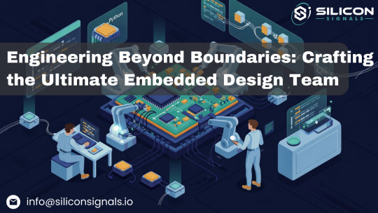
Engineering Beyond Boundaries: Crafting the Ultimate Embedded Design Team
Welcome to the dynamic world of Silicon Signals, where engineering brilliance meets innovative precision. As a trusted partner in embedded systems design, we redefine what it means to build exceptional embedded solutions for global manufacturing excellence. Whether it's breathing life into legacy systems or crafting ground-breaking designs from scratch, Silicon Signals is your strategic partner in navigating the complexities of modern product development.
In an era where technological evolution is non-negotiable, Our commitment to engineering excellence empowers clients to push the boundaries of manufacturing efficiency.
The Embedded Design Lifecycle: From Concept to Reality “Design is not just what it looks like and feels like. Design is how it works.” — Steve Jobs.
At the heart of every successful product is a meticulously structured design cycle. Our approach encompasses every phase—from initial concept to system architecture, hardware design, software development, prototyping, and rigorous testing. This comprehensive process ensures that every product is engineered to meet the highest standards of quality, performance, and functionality.
Silicon Signals' Unique Value Proposition in Embedded Design In an age where embedded technology forms the backbone of modern innovation, Silicon Signals delivers cutting-edge solutions tailored for diverse industries. From precision-driven medical devices to resilient military systems, from the intricate web of IoT in industrial automation to the sophistication of aerospace technology—our expertise transcends industry boundaries.
1. Advanced Firmware and Software Services Our strength lies in the development of innovative embedded firmware and software solutions. Our team of skilled engineers focuses on optimizing system-level programming to achieve an ideal balance between performance, cost, and design aesthetics. This tailored approach aligns with global industry standards, positioning us as a strategic partner capable of delivering excellence at every stage.
2. Comprehensive End-to-End Product Design Solutions We pride ourselves on providing holistic embedded product design services. Our commitment spans from conceptualization to deployment, catering to product development companies and OEMs across the globe. By meticulously managing every phase of the product lifecycle, we ensure seamless integration and a final product that surpasses client expectations.
3. Cost Optimization and Technical Viability In the competitive landscape of embedded systems, cost efficiency and technical feasibility are crucial. At Silicon Signals, we integrate engineering analysis, innovation, and prototyping to offer optimal solutions. Our forward-thinking approach ensures clients receive cutting-edge technology at the most competitive cost, positioning us as the partner of choice for embedded design excellence.
Silicon Signals' Approach to Embedded Design: A Strategic Framework
Our structured methodology provides clients with a clear understanding of their projects at every stage. Key phases include:
1. Ideation: We begin by evaluating technical feasibility and project viability, delivering a detailed Statement of Work (SOW) outlining core features.
2. Engagement Model and Execution Strategy: A well-structured project management approach ensures seamless execution, aligning with client expectations.
3. Industrial Design: This phase encompasses aesthetic design, 3D modeling, enclosure prototyping, and mass production readiness.
4. Hardware Design: Our hardware team focuses on robust architecture, including schematic design, PCB layout, fabrication, and final assembly.
5. Software Development: From firmware to application development, our software engineers optimize performance through meticulous code architecture and testing.
6. Integration and Validation: Comprehensive integration testing ensures that every product functions as intended.
7. Prototyping and Production: We ensure a seamless transition to manufacturing, minimizing downtime and maximizing efficiency.
8. Continuous Support: Our commitment doesn’t end with project completion. We provide ongoing support to ensure lasting performance and reliability.
What Sets Silicon Signals Apart?
1. Market Insights: Our market research ensures that our solutions remain aligned with industry trends and client needs.
2. Expert Engineering Team: Our highly skilled engineers are dedicated to delivering innovative embedded solutions with unmatched precision.
3. Dedicated Technical Support: We offer continuous technical support, providing clients with peace of mind throughout the project lifecycle.
4. Timely Project Delivery: We prioritize efficient project execution, recognizing that time-to-market is crucial in product development.
Partner with Silicon Signals for Embedded Excellence In a world where innovation defines success, Silicon Signals stands as a reliable partner for those seeking to revolutionize their embedded systems. With a structured design cycle, expert team, and unwavering support, we empower our clients to lead in the fast-paced world of technology. Elevate your product development journey with Silicon Signals and experience embedded design like never before.
For sales inquiries, email [email protected] . Visit our website and fill out the query form to learn more.
#embeddedtechnology#embeddedsoftware#embeddedsystems#androidbsp#linux kernel#android#linuxdebugging#aosp#iot development services#iotsolutions
0 notes
Text
The Evolution of PCB Manufacturing: From Basics to High-Performance Boards
PCB manufacturing has evolved from single-layer boards to high-performance, multi-layered designs, enabling innovation in automotive, healthcare, telecommunications, and aerospace. Learn how cutting-edge PCB technologies support modern electronics and drive UK industries forward. Explore advanced PCB solutions for your business today.
#PCB manufacturing evolution#high-performance PCBs#multi-layer PCB design#PCB for 5G networks#advanced PCB technology#UK PCB industry#flexible PCBs#PCB signal integrity#automotive PCB solutions#medical device PCBs#aerospace PCB manufacturing#PCB miniaturisation#HDI PCBs#thermal management in PCBs#next-gen PCB solutions#A-Gas Electronic Materials
0 notes
Text
Global Low Dielectric Materials Market Analysis: Key Players & Innovations
Analyzing Market Trends, Key Players, and Technological Innovations Driving the Low Dielectric Materials Industry Forward.

The Low Dielectric Materials Market Size was valued at USD 1.61 billion in 2023 and is expected to reach USD 2.81 billion by 2032, growing at a CAGR of 6.44% over the forecast period 2024-2032.
The Low Dielectric Materials Market is driven by increasing demand in 5G communication, aerospace, automotive electronics, and high-performance computing. These materials play a crucial role in enhancing signal integrity and reducing transmission loss in high-frequency applications. With the expansion of telecommunications networks, advancements in semiconductor technology, and the rise of IoT and AI-driven devices, the demand for low dielectric materials is expected to surge in the coming years.
Key Players
Leading companies driving innovation and market expansion include:
Daikin Industries Ltd.
Mitsubishi Corporation
Huntsman Corporation
Arxada (formerly Lonza Specialty Ingredients)
SABIC
Asahi Kasei Corporation
Topas Advanced Polymers
Zeon Corp.
Chemours Company LLC
DIC Corporation
Future Scope
As industries move towards faster, more reliable electronic systems, the demand for low dielectric constant (Dk) and low dissipation factor (Df) materials will continue to rise. The rollout of 6G networks, advancements in satellite communication, and the increasing complexity of AI and high-frequency circuits are expected to fuel further innovation in the market. Additionally, the shift towards lightweight, high-performance, and sustainable materials presents significant growth opportunities.
Emerging Trends in the Low Dielectric Materials Market
The industry is experiencing several key trends:
5G and Beyond: Growing deployment of 5G base stations and high-speed networking is accelerating demand for low dielectric materials in printed circuit boards (PCBs) and antenna substrates.
Advancements in Semiconductor Packaging: Innovations in chip packaging and high-frequency semiconductors are pushing the need for materials with superior electrical insulation.
Rise of High-Performance Computing: Increased adoption in data centers, AI processors, and quantum computing is expanding market opportunities.
Aerospace and Automotive Growth: Enhanced applications in radar systems, satellite communication, and electric vehicles (EVs) are boosting industry expansion.
Sustainability Initiatives: Development of eco-friendly, low-loss materials to reduce environmental impact and improve energy efficiency.
Key Points
The Low Dielectric Materials Market is projected to grow at a CAGR of X% from 2024 to 2030.
Increasing demand in 5G infrastructure, aerospace, and advanced computing is a major market driver.
Asia-Pacific dominates the market, with significant growth in North America and Europe.
Sustainable, high-performance materials are gaining attention amid global environmental concerns.
Ongoing R&D efforts are leading to the development of materials with lower dielectric loss and improved thermal stability.
Conclusion
As the world embraces next-generation communication, AI-driven technologies, and advanced computing, the Low Dielectric Materials Market is set for strong and sustained growth. Companies investing in high-performance, sustainable, and application-specific materials will gain a competitive edge in this evolving landscape. With the continuous evolution of wireless networks, aerospace technology, and semiconductor advancements, the demand for low dielectric materials will remain a critical component of the future electronics ecosystem.
Read Full Report: https://www.snsinsider.com/reports/bonding-sheet-market-2554
Contact Us:
Jagney Dave — Vice President of Client Engagement
Phone: +1–315 636 4242 (US) | +44- 20 3290 5010 (UK)
#Low Dielectric Materials Market#Low Dielectric Materials Market Size#Low Dielectric Materials Market Share#Low Dielectric Materials Market Report#Low Dielectric Materials Market Forecast
0 notes
Text
How Flexible PCBs Are Transforming Wearable Tech: A Comprehensive Guide?
The world of wearable technology has experienced a emotional change in later a long time. From wellness trackers to smart watches and indeed health-monitoring gadgets, the integration of progressed electronic components has cleared the way for more brilliant, more compact, and exceedingly productive gadgets. In this comprehensive direct, we will investigate how Flexible PCBs are changing the wearable tech industry, and how PCB Board Fabrication and PCB Fabrication Manufacturers are playing a vital part in this evolution.
How Flexible PCBs Are Affecting Wearable Tech
Wearable gadgets, by nature, require to be compact, lightweight, and comfortable, and conventional rigid PCBs regularly come up short to meet these prerequisites. This is where Flexible PCBs come into play. Their capacity to twist and adjust to the interesting shapes of wearable implies they can be coordinates into more slender, more ergonomic plans. Here's how Flexible PCB are changing wearable tech:

1. Compact and Lightweight Designs
One of the essential points of interest of Flexible PCBs is their capacity to decrease the estimate and weight of wearable gadgets. With Flexible circuits, Manufacturers can decrease the in general thickness of the gadget, making it more comfortable for clients. Whether it's a wellness tracker or a smart watch, wearable gadgets with Flexible PCBs can accomplish thin profiles without relinquishing performance.
2. Solidness and Reliability
Wearable tech gadgets are uncovered to consistent development and stretch from day by day exercises. Flexible PCBs can withstand these conditions distant superior than conventional inflexible PCBs since they are planned to flex without breaking or causing circuit disappointment. The Flexible nature of these PCBs makes them perfect for gadgets that require tall strength, particularly those utilized in extraordinary conditions such as open air sports or health-monitoring wearables.
3. Improved Execution in Constrained Space
Wearables have constrained genuine bequest, and each component needs to be optimized for execution and space proficiency. Flexible PCBs permit for more complex circuit plans to be pressed into littler spaces without compromising usefulness. This is basic for gadgets that require to incorporate sensors, processors, remote communication modules, and batteries in a compact frame factor.
4. Made strides Plan Flexibility
With Flexible PCB technology, architects are no longer constrained by the imperatives of rigid circuits. They can coordinated more components in unusual ways, giving a part more room for imaginative plans. This opens up unused conceivable outcomes for making more personalized and customized wearable gadgets that can oblige highlights such as bended screens or multi-functionality.
Role of PCB Fabrication Manufacturers
The part of PCB Fabrication Manufacturer is basic in bringing the potential of Flexible PCBs to life. These Manufacturers utilize progressed procedures in the Fabrication of Flexible PCBs, counting multi-layer stacking, exactness carving, and robotized get together forms. Their mastery guarantees that Flexible PCBs are tough, dependable, and competent of assembly the execution necessities of the most recent wearable tech devices.
When working with Flexible PCBs, PCB Manufacture Manufacturers must too guarantee that the materials utilized are of the most elevated quality to anticipate issues like delaminating or splitting, which can influence the long-term execution of the wearable devices.
Conclusion
The rise of Flexible PCBs is without a doubt one of the most critical improvements in the wearable tech industry. These progressed circuit Boards empower Manufacturers to make littler, lighter, and more tough gadgets that offer upgraded usefulness and superior execution. As the request for wearable gadgets proceeds to develop, the part of PCB Fabrication Manufacturers will as it were gotten to be more basic in guaranteeing that Flexible PCBs meet the thorough measures of cutting edge technology. The future of wearable tech is certainly Flexible, and Flexible PCBs are at the heart of this advancement.
0 notes
Text
Test Engineering in Industry 4.0: The Shift Towards Smart Manufacturing

Manufacturing has been revolutionized by Industry 4.0, where digital innovations seamlessly unite with traditional processes, resulting in a world where automation, precision, and data-driven decision making prevail. In this article, we will see how test engineering has progressed to meet the modern production challenges, leveraging the emerging advanced testing methods, stringent quality assurance, and smart automation practices that are propelling production systems worldwide for reliable, efficient, and innovative manufacturing today.
Evolution of test engineering
The field of test engineering has transformed over the past decades as industries embraced digital innovations. Sophisticated techniques have replaced traditional methods to maintain efficiency and reliability. Adapting to increasing product complexity and dynamic market requirements has been driven by the evolution in test engineering and management. In manufacturing systems where sensors, data analytics, and automation are integrated, rigorous testing has become critical to operational success. This shift not only improves product quality but also optimizes processes by pinpointing problems early in the production cycle. Today, engineers use integrated software tools to monitor performance, simulate, and validate results in real time. The industry has been committed to innovation and quality control, resulting in the continuous improvement of testing protocols that have led to safer, more reliable products. With a focus on modern test engineering practices, they are a cornerstone in the transition to a data driven manufacturing ecosystem. The legacy they left behind continues to inspire future advancements across sectors worldwide.
Digital transformation in manufacturing
Manufacturing has been transformed by digital transformation, which has combined advanced computational methods and conventional industrial practices. Automation and real time data analytics have made operational workflows faster, smoother and error free. A robust engineering design testing process is essential to ensure that digital systems meet high quality and performance requirements. Engineers leverage digital twins alongside simulation models and cloud computing to forecast system behavior across different operational scenarios before starting production. The proactive nature of this approach shortens equipment downtime while enhancing total operational efficiency. Digital transformation allows companies to optimize resources, monitor system integrity continuously, and be able to adapt to market fluctuations at high speed. The convergence of digital technologies in manufacturing not only speeds up the process of innovation but also improves quality assurance protocols, making manufacturing processes more efficient and sustainable. If we want to achieve operational excellence and be successful over the long term in a competitive landscape, modern testing methodologies need to be integrated. It underscores the revolutionary impact of technology in manufacturing efficiency and product integrity.
Integration of automation systems
Modern manufacturing has achieved unprecedented efficiency and consistency through the implementation of automation systems. Modern manufacturing relies on automated processes to manage complex operations previously handled by humans which leads to faster production cycles and reduced errors. A thoughtfully designed PCB design board becomes crucial when multiple automation components need to communicate because it enables smooth data exchange between sensors, actuators and controllers. The combination of hardware and software creates real-time monitoring capabilities that enable adaptive control systems which sustain optimal performance levels. Automation technologies enhance both workflow optimization and data-driven decision support systems. Smart manufacturing development continues to rely on intelligent machinery integration with robust control systems to enhance operational efficiency. The integration of these elements establishes a fundamental base for developing flexible production environments that offer scalable capabilities and resilience to market changes. The PCB design board will remain central to future automation progress as new innovative approaches improve system interoperability and operational efficiency.
Advancements in quality assurance
Recent advances in quality assurance have changed the manufacturing landscape, emphasizing precision and reliability. Modern testing methodologies are strategically integrated to consistently meet rigorous industry standards. This framework of test engineering and management stands as a cornerstone to this evolution, balancing process control with technological innovation. Quality assurance protocols are constantly refined through the application of advanced analytics and machine learning to detect anomalies and mitigate risks. The result has been dramatic reductions in production defects and increased overall production efficiency. Automated inspection systems and predictive maintenance are now used in quality control to forecast potential failures before they occur, guaranteeing sustained performance. This makes manufacturers better positioned to provide superior products at less waste and greater resource utilization in a competitive marketplace. Additionally, continuous improvement practices promote process transparency and reliability, which in turn creates an environment where test engineering and management principles enable decision making and innovation. This systematic approach leads to production operations with enduring quality and sustainability.
Innovations in engineering design
Catalyzed by innovative approaches in engineering design, manufacturing methodologies have evolved into an era of precision and adaptability. The importance of the engineering design testing process has been emphasized on structured frameworks to evaluate each prototype thoroughly. This paradigm allows engineers to simulate real world conditions, assess structural integrity, and optimize design parameters before production. In this dynamic landscape, collaboration among multidisciplinary teams is essential to leverage insights from different areas to uplift the overall product performance. Design innovations are not only functional but also allow for increased cost efficiency and environmental sustainability. Advanced software tools and simulation platforms further strengthen the reliability of design outcomes in modern manufacturing facilities. Thus, companies are able to manufacture innovative and robust products that meet market demands and raise the bar for industry standards through continuous improvement and rigorous testing protocols. The engineering design testing process is further reinforced with continuous feedback loops and iterative refinements to provide reliability and optimum product performance.
Future prospects and challenges
The upcoming era of smart manufacturing shows promise but simultaneously presents multiple obstacles to overcome. Technology advancements transform production processes while driving new problem-solving methods. The growing complexity of modern systems demands better integration between digital tools and automation frameworks. The success of modern systems depends heavily on well-engineered PCB design boards that maintain both operational reliability and effective connectivity. The future of manufacturing will benefit from artificial intelligence alongside augmented reality and predictive analytics to drive advanced process optimization. However, issues such as cybersecurity, data integrity, and scalability present ongoing hurdles. The industry needs to overcome these obstacles while sustaining dedication to quality standards and innovation. Strategic partnerships combined with ongoing research will shape the next manufacturing era through adaptable production systems and resilient manufacturing environments. Research and development investments will continue to resolve emerging issues while strengthening the PCB design board's role in connecting technological advancements to dependable manufacturing processes.
The convergence of technology, rigorous testing, and innovative design defines smart manufacturing. Test engineering has evolved to change production with efficiency and quality. Digital solutions and robust automation are still being embraced by industry professionals. Continuous progress and focused improvements assure the future of manufacturing, securing reliability and excellence in the production process in every phase, worldwide today.
0 notes
Text
The World’s Gold Chloride Powerhouses: Top Countries Shaping the Market
According to a recent research, Industry revenue for Gold Chloride is expected to rise to $343.8 million by 2035 from $143.0 million of 2024. U.S., Germany, China, Japan and UK are the top 5 markets and combinely holds substantial demand share. The revenue growth of market players in these countries is expected to range between 6.1% and 8.7% annually for period 2025 to 2035.
Industry transition including the rise of nanotechnology and evolution towards green chemistry, are transforming the supply chain of Gold Chloride market. The growing use of gold chloride in nanotechnology has brought about a change in the industry by playing a crucial role in creating gold nanoparticles used in various applications such as drug delivery and bioimaging in healthcare and electronics sectors as well as theranostics field. This shift has had an influence on industries like healthcare, electronics and textiles due to the rising need, for cutting edge nanotechnologies propelling the expansion of the gold chloride market.
Potential Application Areas
Pharmaceutical Industry: The use of gold chloride in the pharmaceutical industry is significant. Commonly involves auric chloride . AuCl₃ shows promise in the creation of cancer medications as it can hinder the growth of cancer cells. This unique attribute has garnered interest from companies and has become a key element in the production of oncology drugs by major players, like Roche and Pfizer.
Electronics Industry: In the field of electronics manufacturing industry utilizes gold chloride primarily in the production of printed circuit boards . In this process a diluted form of gold chloride along with substances is employed to apply a fine gold layer, on the PCB surfaces to improve their conductivity and protect against corrosion.
Industry Leadership and Strategies
The Gold Chloride market is characterized by intense competition, with a number of leading players such as Sigma Aldrich, Strem Chemicals Inc, William Rowland Limited, Finar Limited, Bennett Scientific, ACROS Organics, Surepure Chemetals, GFS Chemicals, TCI Chemicals, Spectrum Chemical, Nippon Soda Co Ltd and Alfa Aesar.. These players are pushing the boundaries of innovation & technological advancements and forging strategic partnerships to expand the existing reach of the market. Below table briefs about adopted market strategies by leading players.
Access detailed report insights here - https://datastringconsulting.com/industry-analysis/gold-chloride-market-research-report
About DataString Consulting
DataString Consulting assist companies in strategy formulations & roadmap creation including TAM expansion, revenue diversification strategies and venturing into new markets; by offering in depth insights into developing trends and competitor landscapes as well as customer demographics. Our customized & direct strategies, filters industry noises into new opportunities; and reduces the effective connect time between products and its market niche.
DataString Consulting is a professional market research company which aims at providing all the market & business research solutions under one roof. Get the right insights for your goals with our unique approach to market research and precisely tailored solutions. We offer services in strategy consulting, comprehensive opportunity assessment across various sectors, and solution-oriented approaches to solve business problems.
0 notes