#Printed circuit board design software
Explore tagged Tumblr posts
Visit Tumblr Blog
Explore Tumblr blogs with no restrictions, modern design and the best experience.
Last Seen Tumblr Blogs


Fun Fact
There were a total of 171.5 billion posts on Tumblr in 2019.
Text
Helpful Analysis of the Latest Printed Circuit Board Design Software
Navigating the ever-evolving landscape of PCB technology demands the right tools, especially when working with prototype circuit board projects that require precision and efficiency. Quick turn PCB fabrication plays a vital role in accelerating innovation and cutting down lead time, making modern design tools indispensable for engineers and developers.
Enhancing Accuracy Through Structured PCB Design
To streamline complex circuits and ensure optimal performance, structured design methods offer better control and consistency. These strategies are essential for professionals working on intricate PCB layout design or utilizing advanced printed circuit board design software to meet tight development cycles. From seamless design integration to real-time collaboration, today’s software solutions empower engineers to move from concept to final board faster. Bay Area Circuits supports innovation with services like high-quality prototype production and rapid assembly. Visit their website and explore their services.
For more reading, Visit here - https://67d7ed103fe91.site123.me/blog/helpful-analysis-of-the-latest-printed-circuit-board-design-software
#Quick turn PCB fabrication#prototype circuit board#PCB layout design#printed circuit board design software
0 notes
Text
PCB Manufacturing in Toronto: Expertise, Services, and Local Industry Insights
Discover PCB manufacturing in Toronto, a hub of innovation and quality in electronic manufacturing services. Learn about the specialized capabilities, technological advancements, and diverse offerings of PCB manufacturers Toronto. Explore how local expertise and cutting-edge facilities contribute to producing high-quality printed circuit boards for various industries and applications worldwide. For more details visit our website www.crimpcircuits.com
#pcb manufacturing toronto#printed circuit board design#metal clad pcb#printed circuits#rigid flex pcb#full turnkey pcb services#turnkey pcb services#pcb parts#eagle software#pcb designing#flexible pcb#pcb assembly#printed circuit board manufacturers#pcb manufacturers in canada#circuit board manufacturers in canada#pcb quote#pcb prototype services in canada
2 notes
·
View notes
Note
Cactus fascinates me, does it run on code similar to an existing instruction set or is it completely original on that front?
What can you do with it? What's it's storage?
Both the Cactus (the original wooden prototype from years ago) and the new PCB Cactus(es) are essentially derived from a minimal 6502 computer design by Grant Searle for their core logic. Here's what that would look like on a breadboard:
There isn't much to it, it's 32K of RAM, 16K of ROM containing Ohio Scientific's version of Microsoft BASIC, a 6850 ACIA for serial interaction, some logic gates, and of course a 6502 microprocessor (NMOS or CMOS, doesn't matter which). You hook it into a terminal and away you go.
Grant's design in turn can be best described as a distilled, modernized version of the OSI Challenger series of computers. Here's an OSI-400 and a Challenger 4P respectively:

The left one is a replica of the 400 circa 1976, also called the Superboard. It was affordable, endlessly reconfigurable and hackable, but ultimately very limited in capabilities. No BASIC, minimal monitor ROM you talk to over serial, but you could connect it to a bus to augment its features and turn it into a more powerful computer.
Whereas the OSI C4P on the right from about 1979 has more RAM, a video card, keyboard, BASIC built in, serial interface, cassette tape storage, and that's just the standard configuration. There was more room to expand and augment it to your needs inside the chassis (alot changed in 3 years for home computer users).
Grant's minimal 6502 design running OSI BASIC is a good starter project for hobbyists. I learned about the 6502's memory map decoding from his design. I modified and implemented his design on a separate cards that could connect to a larger backplane.
Here are the serial, ROM, RAM, and CPU cards respectively:
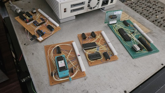
Each one is 100% custom, containing many modifications and fixes as I developed the design. However, that's only half of the computer.
I really wanted a 6502 machine with a front panel. People told me "nobody did that", or couldn't think of examples from the 1970s but that seemed really strange to me. Especially since I had evidence to the contrary in the form of the OSI-300:
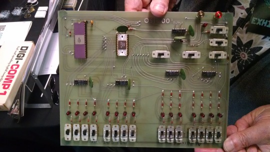
This one I saw at VCF West back in 2018 illustrates just how limited of a design it is. 128 bytes of RAM, no ROM, no serial -- just you, the CPU, and toggle switches and LEDs to learn the CPU. I was inspired the first time I saw one in 2015 at VCF East, which is probably when this whole project got set in motion.
Later that year I bought a kit for a miniature replica OSI-300 made by Christopher Bachman, and learned really quickly how limited the design philosophy for this particular front panel was. It was a major pain in the ass to use (to be clear, that's by OSI's choice, not any fault of Christopher in his implementation)

So... I designed my own. Took awhile, but that's the core of what the Cactus is: my attempt at experiencing the 1970s homebrew scene by building the computer I would have wanted at the time. Over half of the logic in the Cactus is just to run the front panel's state machine, so you can examine and modify the contents of memory without bothering the 6502. I added in all of the things I liked from more advanced front panels I had encountered, and designed it to my liking.
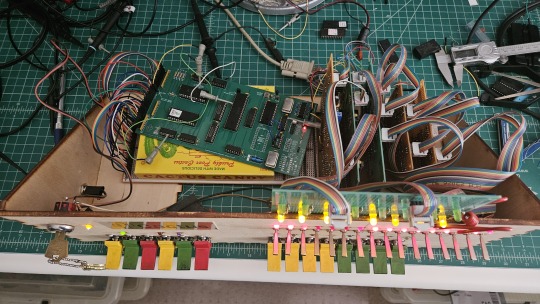
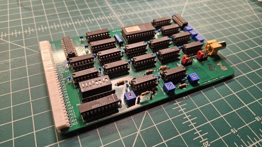
Here's the original front panel, accompanying logic, and backplane connected to the modern single board computer (SBC) version of the machine:
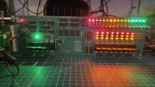
And here's the new Cactus SBC working with the new front panel PCB, which combines the logic, physical switch mountings, and cabling harnesses into a single printed circuit board.
So, what can you do with it? Pretty much the same things I do already with other contemporary 1970s computers: play around in BASIC, fire up the occasional game, and tinker with it.
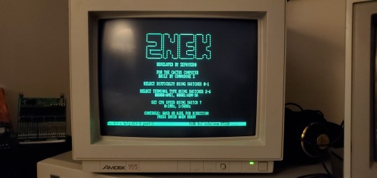
I've got no permanent storage designed for the Cactus as yet, it's been one of those "eventually" things. The good news is that a variety of software can be ported to the hardware without too much trouble for an experienced hobbyist. A friend of mine wrote a game called ZNEK in 6502 assembly which runs from a terminal:
Right now, you have to either toggle in machine programs from the front panel from scratch, burn a custom ROM, or connect it to a serial terminal to gain access to its more advanced features:

Here's it booted into OSI BASIC, but I have also added in a modern descendant of Steve Wozniak's WOZMON software for when I need to do lower level debugging.
I've also got a video card now, based on the OSI-440. I have yet to implement a keyboard, or modify BASIC to use the video board instead of the serial connection. Even if I did, screen resolution is pretty limited at 24x24 characters on screen at once. Still, I'm working on that...

Anyway, I hope that answers your question. Check the tags below to see the whole process stretching back to 2017 if you're curious to learn more of the project's history. I'm also happy to answer any more questions you might have about the project.
267 notes
·
View notes
Text
On Bodging Silly Mistakes
After a few weeks of rest and working on non-homebrew-related projects since getting my 68030 stack running 8-user BASIC, I've circled back around to the project. My goal is to have it ready to exhibit for VCF Southwest 2025 in June.
The first thing to do when picking up an old project is to make sure it still works to begin with.
It did not.
The computer would start up, go through its boot process, and start the user programs. The supervisor terminal would accept and execute commands, but none of the user terminals would accept input.
I could tell the serial data was making it to the machine, because my 8-port serial card has indicator LEDs on the Transmit & Receive signals and they were working as expected. If I held down a key as the system booted, it would print that character a few times before stopping and then no longer accept any more data. So it really looked like the hardware was working. Nothing had changed in software so that wasn't likely to be the issue.
It reminded me of the problems I encountered with reading from disk when CPU cache was preventing the updated disk status bit from being read. The serial card supports asserting the CPU's Cache Inhibit signal, but perhaps that circuit wasn't functioning. There was no change with it connected or not. Time to break out the oscilloscope. The Cache Inhibit signal was always low — always asserted. Cache wasn't the problem because cache was effectively always disabled.
Out of ideas, it was time to break out the logic analyzer. The I/O Read & Write signals on the serial card were working as expected, and it was properly addressing the card & its individual ports. So next thing was to check was the actual data being read from the UARTs.
Letting the logic analyzer run and watching the data fly through, the problem finally made itself known — the UARTs were not setting bit 0 of the status byte to indicate that they had received data. The data was getting to the UART, it just wasn't acknowledged.
But why? And why did it work initially on restart and then stop? And why did it work without issue a few weeks ago? What is different?
What is different, indeed. I have made one change to the hardware since I last ran it — I added a proper watchdog/power-on-reset controller. If the power supply drops below 4.7 volts, it will reset the computer. The power supply I had been using was marginal and was getting caught by the watchdog, so I switched to a proper power PC supply.
So what's different since last time I ran the system is my reset circuit is more effective and the system voltage should be much more stable 5V.
And that's when I realized a mistake I made in the design for my 8-port serial card. The 68k reset signal is active-low and the 16C55x UART reset signal is active-high. I was trying to minimize part count, and didn't have an inverter for the reset signal, so I used what I had on hand — a buffer with an active-low enable signal.

Anyone well-versed in electronics may already see the problem.
When the CPU-RESET# signal is asserted (low), the buffer will set its output, IO-RESET to match its input, VCC (high). That's great, we get a high signal on the output whenever the CPU Reset signal is low.
Except ... what happens when the CPU Reset signal is not asserted? The buffer goes open-collector and doesn't pull the IO-RESET signal one way or the other; it's just left floating.
Floating signals are bad news for digital circuits. Their behavior is unpredictable and subject to environmental noise, power fluctuations, etc. For my IO-RESET signal to function properly, something needs to pull it low whenever the 74'125 buffer is not actively driving it high. A good-sized pull-down resistor should do the job just fine, so I dug through my stock and found a 3.65k surface-mount resistor and bodged it onto the back side of the board.

And sure enough, that fixed the problem!
It is possible that when I was running the system on that marginal power supply previously, the IO-RESET signal was able to stay just low enough to not trigger reset on the UARTs. Or it could have just been different environmental factors.
I'm glad I took the time to test the machine today, and I'm glad this bug came up. It's the kind of bug that could easily have come up when running in a new environment for the first time — such as on the show floor at VCFSW. Far better to run into a bug like this at home with access to all of the tools (and time) to figure it out.
Now that things are up and running again I can continue my testing and setup for VCFSW.
#homebrew computing#homebrew computer#vintage computing#motorola 68030#motorola 68k#mc68030#wrap030#vcfsw
16 notes
·
View notes
Text

Giving Tuesday – KiCad open-source design #GivingTuesday 💻🔧🌍❤️🤝
KiCad is an open-source software suite for electronic design automation (EDA), enabling users to design schematics and printed circuit boards (PCBs). KiCad is a great, free, open tool for creating complex designs, from hobbyist projects to professional-grade hardware. As an open-source initiative, KiCad promotes accessibility and collaboration, making advanced EDA tools freely available. Supporting KiCad helps the development of features, bug fixes, and community-driven improvements, empowering engineers, educators, and hobbyists worldwide. Consider donating to KiCad to strengthen the open-source hardware community and help make high-quality EDA tools accessible to everyone.
In the past year, they posted this nifty chart that shows what your support can help accomplish.

If KiCad is valuable to you, please consider donating to help make it even better.
#kicad#kicadpcb#electronics#eda#schematic#pcbdesign#pcblayout#opensource#edatools#openhardware#donatetoday#engineeringdesign#communitysupport#openedsystems#opensourcecommunity#pcbtools#givingback#generositymatters#techforgood#makercommunity#electronicsdesign#designsoftware#kicaddonation#hardwaredesign#opensourceinitiative#techcommunity#sharekindness
11 notes
·
View notes
Text
Understanding Electronics Design & Engineering

Introduction
Electronics design engineering is that critical component that determines the future of innovative products in a competitive tech industry today. It consists of all services—from concept development in the initial stage to the final testing of the product, so as to deliver an electronic product capable of high performance and meeting the established performance standards as well as regulatory compliance. This amalgamation of experience and approach in the area of hardware, firmware, mechanical design, and regulatory compliance underlines electronics design engineering as a fundamental component in the development of reliable and efficient products.
Concept development
It is the first phase of the process in electronics design engineering. Concept development is that phase that involves the idea generation of a product, an analysis of needs in the market, and, by extension, setting the technical requirements for the product. Engineers and designers can then work together to create a solid proposal for the product development so that concept development becomes both market-worthy and technically viable.
Firmware development
It is a part and parcel of electronics design engineering because it explains how the hardware would interact with the world outside. It deals with the embedded software, which makes sure that the hardware components work smoothly and seamlessly.
The prime areas involved in firmware development are as follows:-
Embedded Systems: The firmware is tailored to regulate the internal systems of a device.
Real-Time Processing: The firmware is designed considering the real-time processing of data; this leads to responses that are swift and reliable.
Customization: Engineers design the firmware to specifically correspond with the product's functionality and application.
Want to take your product to the next level with custom firmware? Get in touch with Lanjekar Manufacturing today for more information on how our electronics design engineering services can help.
Hardware Development
In electronics design engineering, the development of hardware is an important stage wherein engineers design the physical components that bring electronic devices to life. Hardware has to be robust and reliable and to enable the firmware for the optimal performance of the product.
Some of the important steps in it are as follows:
Component selection: High-quality components have to be selected according to the technical specifications of the product to be designed.
Prototyping: Engineers must make prototypes to check if the designs are valid and free from potential dangers that might eventually come into operation in full-scale production.
Testing: Extensive testing is carried out in this stage to test the functionality and life expectancy of the hardware.
PCB Layout Design
Printed circuit boards (PCBs) are the backbone of any electronic product, and hence their design must be correct. PCB layout design in electronics design engineering refers to the designing of efficient, interference-free, and compact designs within the form of the product.
Key considerations involve:
Schematic Design: The engineers produce an in-depth diagram to represent how one component connects to another.
Layout Optimization: It optimizes the layout so that signals remain robust and interference potential is minimized.
Manufacturability: The design is optimized with best practices that ensure efficient production of PCBs.
Regulatory Compliance and Certification: Ensure the product meets local and international standards, this is part of the work of electronics design engineering. This includes:
Knowledge on Regulatory: Engineers ensure that the product goes through the required regulations, safety, and environmental standards.
Testing: Testing of products to conform to the certification through acquisition of compliance standards.
Documentation: All these supporting documents for certifications undertaken in the engineering process. Mechanical DesignIt is one thing to have a good internal part of the device, but the mechanical design of a product cannot be overlooked. Electronics design engineering typically incorporates mechanical design in its design to ensure that the device has a good, robust structure that appears aesthetically pleasing.This is what constitutes mechanical design, such as;
3D Modeling: Engineers create 3D models that would allow the individual to visualize the physical structure of the product.Thermal Management: Effective thermal design, where the hot elements are dissipating the heat away.
Material Selection: Correct material to utilize for ruggedness, weight, and functionality
Mechanical Design: It is also critical to ensuring the product functions well but with ease of usage.
Connectivity Solutions
With the increasing rise in the deployment of IoT products, electronics design engineering puts emphasis on connectivity solutions. This could either be wireless or wired. This ensures that the product is communicating effectively.
Some of the crucial considerations include the following:
Protocol Implementation: It ensures total compatibility with different communication protocols like Wi-Fi, Bluetooth, or Zigbee.
Seamless Integration: The connectivity solutions are also made to not compromise with the performance of a product.
Security Measures: Connectivity solutions also deal with data security, one important feature of modern devices.
Conclusion
Electronics design engineering contains all aspects of product development, from concept to compliance. The discipline of electronics design engineering consists of focusing on firmware, hardware, PCB layout, mechanical design, and connectivity, ensuring the end product is reliable, innovative, and compliant with industry standards. If all the components can work well coherently, it doesn't only produce a friendly user at the end but also something that will be in high demand in the market.
Contact Lanjekar Manufacturing today and share your project with us to find out how we can give your ideas life.
Also read:
Know Electronics Manufacturing: The Total Guide
Firmware Development: Where Software Meets Hardware
The Essentials of PCB Design: Techniques and Best Practices
The Complete Guide to Hardware Development: From Design to Deployment
2 notes
·
View notes
Text
A controller with a scroll wheel, you say?
Well this is a little funny. Yesterday I posted the first part of a series of post on the fine details of how computers work, mentioning how I've been looking into this as part of a personal project I've been working on, and today I wake up to see Masahiro Sakurai posting a youtube video lamenting the lack of... this exact thing I'm working on.
Apologies for how much cat hair is in this photo, that's a bit of an occupational hazard, but this here is a photo I took back in September when most of the parts I had to order were in for the prototyping of this thing:
That's a really bad MS Paint mockup, but yeah. I'm designing my own game console, and one of the key features is a big ol' scroll wheel right in the center of the controller. Another is that I'm planning to just put all the designs of the circuit boards and 3D printer files for the casing/buttons up online for free, making it this totally open DIY thing where anyone who's a big enough nerd can just make a couple downloads, order some dirt cheap components, and build their own copy of the system (or people with better setups than me can build and sell them, whatever). So I'm not super worried about anyone stealing my ideas or whatever, but I WOULD like to establish a standard and all that, and figured it was worth noting that this is something I've been slowly working towards for like a year or two now, and didn't just get the idea from this video:
youtube
But yeah, now that the idea's out in the public consciousness, here's the plan for the controller (that I was planning to keep under my hat until I had a working prototype and some demo software sometime next year).
First off, the plan is that this is to be the standard controller for a whole console I'm also plucking away at designing, which is a bit more ambitious of a project, so I figure I might as well make it compatible with something that's already out there. So specifically, I'm designing this so that you can take one, plug it right into an SNES (or with a different connector at the end, an NES, because turns out they use the exact same input handling standard and it's just the shape of the plastic on the end that differs), and have it just work. Or mostly work anyway. I'm hoping I can process a signal out of the scroll wheel in a way that it either just needs the 3 extra bits of the input signal I don't have buttons for in my design (more on that later) or failing that, I can get it to output the same sort of signal as one wheel in the SNES mouse, which just rides along the second data line very few things use. I think that plan might break multitap compatibility and require an extra chip on the controller PCB, but it would leave this slightly more compatible with existing games on the same hardware. I might also do something weird with the button mapping to be sure NES select is on a shoulder and it works right out of the box with that whole library.
Working out exactly how to handle signals from the scroll wheel happens to be the point I'm currently stuck on by the way. I got this baggie full of rotary encoders for just a few cents which... almost fit in my first draft 3D printed wheel housing, but I have NO documentation on them, not even a part number/manufacturer besides "H-9," the pins don't fit a breadboard, and I've kinda been scrambling for rent so I can't afford a nice multimeter or oscilloscope to poke around with. Plus again I need to redesign this wheel print to even get it to spin right, and... this was a gift from a friend with a printer who is Not Local. Solvable problem, just needs more time and/or outside expertise.
But yeah, once I have those kinks worked out, it should be easy enough to get a custom board design made, replicas of end-cap of the controller cord are another problem easily solved by ordering a 1 dollar part or 3D printing something. The actual cord might be tricky since I don't know where you actually order something like that from, but it should be easy enough for anyone who doesn't mind a little assembly work to put one of these together and have it good to go for any software made with it in mind, or retrogames where you don't mind a weird button count. So... what's the pitch on this scroll wheel anyway?
Well for starters, there's the stuff Sakurai got into this morning. Any sort of RPG or text heavy game can use it to quickly scroll through menu options, or stuff in a text-heavy game. You could also pan the screen with it, something a lot of early 16-bit games assigned to the shoulder buttons or holding up and down while getting used to the new options the hardware was giving them.
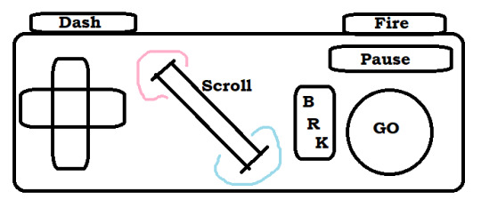
Past that, you'll notice in my design it's at a 45 degree angle. I might have to tweak it a little, but my thinking is for a game that uses it heavily, one thumb or the other can slide over easily enough (I'm going for a pretty compact overall design) so we can have some games where you take your thumb off the D-pad, and have this nice analogue steering wheel. Nice for fine control in a racing game, or if you want some little radio-tuning/safe-cracking sorta deal.
Alternatively, move your right thumb over, use the D-pad to steer, shoot and dodge or whatever with shoulder buttons, and use the wheel to rotate a turret for a twin-stick sort of game maybe.
Or just use it for the sort of stuff mouse based games stick on the scrollwheel. Changing weapons, changing powerups... I'm planning to officially label the directions "hot" and "cold" to encourage weird gimmicky things like... I dunno, a platformer where you have a thermostat in your controller you can always mess with, freeze water coming out of pipes, crank up flame jets? Have a shot charging mechanic where you just really crank it to get to max strength? Weird minigame stuff. There's some fun space to explore with it.
Then we have the rest of the design here... which basically comes down to me being just plain sick of how every controller made by anyone in the past... 20 years give or take has kind of the exact same layout? 4 good face buttons, a D-pad, 4 shoulder buttons, 2 sticks, and 1-4 annoying to reach tiny awkward middle buttons, and we're just kind of overdue for a change-up?
Like first of all, hey, this is just too many buttons. There's a ton of games that really only need a D-pad, and maybe 3 buttons (attack jump pause) and the two things that aren't fully standardized is how awkwardly placed the D-pad is and how awful and awkwardly placed the pause button is. Shoulder buttons can be nice, but I've never really felt like 4 of them awkwardly crammed on the rim has been really useful or ergonomic, and that's coming from someone who's been playing a ton of FF14, which gets more use out of them than anything else I could name. And really, aside from games doing fake twin-stick stuff and using the whole grid like a second D-pad, I'm having a really hard time thinking of any game I've ever played that really makes good use of 4 good face buttons? Like people will use them if they've got'em sure, but unless you do that keyboard style thing where you lay the controller on a table and use all your fingers, you can really only comfortably hit 2 face buttons without sliding your thumb away from them, maybe comfortably make a quick pivot to a third.
Also, really, a lot of designers just sort of feel compelled to map SOMETHING to every button, even if it's clear the design didn't really need them. So basically I figure I'll try kinda just taking a "less is more" approach here. Here's the buttons that it's comfortable to rest your thumbs and fingers on, here's a dedicated pause/menu button where people often stick a kind of redundant menu button, here's my gimmicky scrollwheel. That's it, work around that.
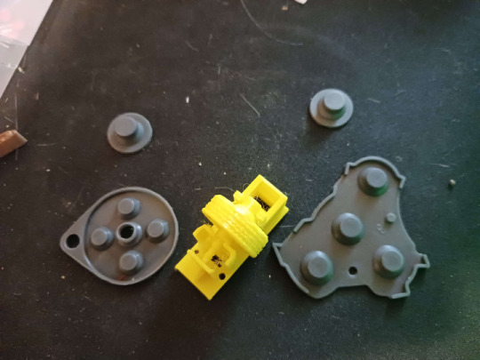
I'm also going a little Gamecube inspired (literally using replacement membranes for one in my prototype design, even). Gonna make a great big primary button and use different shapes for the other two. Trying to label these in a less arbitrary fashion than most. If shooting a gun is a thing you do in this game, and there isn't a real good reason not to, default it to this nice right trigger you can hold down all the time. If we're advancing through menus or jumping or holding down gas in a car, here's the big GO button. Need brakes, need to break stuff with a melee attack? Go back in a menu system? There's your other face button. Have a quick dash move or a run you hold down, let's just use the other shoulder.
So yeah. That's my controller. Need to work out the kinks on the scroll wheel, source a cord, and hopefully I can slap things together and this will be something you can just order bits for piecemeal and put together for like, $5-10 after shipping? Maybe less? The parts are shockingly cheap so far.
But yeah if anyone has any insight to the scroll wheel or cord issues, let me know. Also the whole thing is presently a tad back-burnered because I am in a serious financial crisis and I don't want to have electronics spread all over my table if I have to abruptly find a new place to live if I can't scrape next month's rent together. So as usual, donations are incredibly welcome.
2 notes
·
View notes
Text
The functions of silicon chips and circuit boards are determined by the patterns printed onto them.
These patterns are designed with both text and symbolic languages that look nothing like the final patterns.
Then if you have firmware or software, you have to power everything up and invoke a specific sequence of steps to get the thing to work at all.
Arthur C. Clarke was right.

119K notes
·
View notes
Text
How Proto PCBs and Quality Circuit Boards Parts Accelerate Product Development
PrototypePCB assembly is an innovation that has become a key component in the world of electronics, which is fast-paced and where time-to market plays a major role. These quality printed circuit boards (PCBs), which are produced in a short time, have revolutionized the prototyping procedure. They enable engineers to produce and upgrade Proto PCB at an unmatched rate and effectiveness.
PCBAndAssembly utilizes advanced manufacturing techniques for PCB to reduce production timing from several weeks to hours in multiple scenarios. It allows them to produce quality prototyping and unmatched efficiency in the production unit
Companies can accelerate their product design, reduce their time-to market, and achieve greater success on the electronics market by incorporating PCBs in their development cycle
Prototype PCB Production Using Cutting-Edge Technologies
PCB product (Printed Circuit Boards) is witnessing a transformation driven by new technologies. These are reshaping manufacturing processes. This blog will show you how to prototype your design with a PCB.
Machine Learning and AI
Since the early days of electronics, CNC machining has supported rapid PCB prototyping. AI-powered Design Rule Checking systems (DRC) are revolutionizing PCB Design by detecting flaws at an incredibly high rate of accuracy. These systems constantly improve their detection abilities by leveraging extensive databases of successful design and manufacturing data. This ensures adherence to strict design rules and reduces errors.
ML algorithms adjust manufacturing parameters in real time to account for changes in material properties and environmental conditions. This ensures consistent quality.
Advanced (CAD) Software
CAD also known as Computer-Aided Design is effective software designed for simplifying PCB production process. Your schematics will define the structure of your device, and show you how to connect your components in a coherent way. The PCB is designed in a schematic editor that uses CAD circuit tools to connect and place components in the real device. This increases effectiveness and encourages invention.
On the manufacturing side, engineers at PCBAndAssembly advanced CAM software (computer-aided design) translates design data to machine instructions in a minimal amount of time. This reduces human error and minimizes setup time.
Innovative Materials and Components
The PCB industry is advancing due to recent advancements in circuit board parts and materials. High- speed laminations offer better signal integrity and can support higher clock speeds, denser layouts, and faster clocks without compromising performance. Turnkey results that incorporate embedded components such as capacitors and resistors in the Prototype PCB layers reduce assembly time while improving reliability.
Automated Optical Inspection in Quick Turn PCBs
In the high- speed environment of quality PCB assembly, PCBAndAssembly’s automated optical inspection (AOI), is pivotal for maintaining quality norms. As production speeds rise, so does the risk of errors and defects. AOI is therefore a vital tool to ensure circuit board assembly reliability.
Recent advances in AOI have dramatically increased its effectiveness for high- quality proto PCB manufacturing. Multi-angle cameras with high- resolution can descry blights down to 10 micrometers. Machine learning algorithms improved defect classification accuracy. This reduced false positives, and allowed manual inspections to be performed less often.
0 notes
Text
Introduction to Lin Bus and Special Devices for Electrostatic Surge Protection

1、 Introduction to Lin Bus
A. Definition of Lin Bus
Lin bus is a serial communication bus suitable for communication between automotive electronic control units (ECUs).
B. Characteristics of Lin Bus
The Lin bus adopts a single end drive and differential transmission method, which has the characteristics of high-speed transmission and strong anti-interference performance.
C. Application scope of Lin bus
The Lin bus is mainly used for communication between electronic control units (ECUs) in automobiles, such as engine control units, transmission system control units, body control units, and so on. The emergence of the Lin bus enables data exchange and communication between ECUs of different brands, systems, and functions, thereby improving the overall performance and safety of automobiles.
2、 Problems with Lin Bus
A. Hazards of static surges
Static surges and other factors can damage the performance and stability of the Lin bus.
B. Stability and reliability issues of Lin bus
There are also some problems with the Lin bus in practical applications.
3、 Design of electrostatic surge protection
A. Hardware protection measures
The design of electrostatic surge protection needs to start from both hardware and software aspects. In terms of hardware, measures such as protective circuits can be taken to limit electrostatic surge voltage, such as using protective circuits composed of TVS diodes, inductors, capacitors, etc.
Suggestions for the layout of ESD devices
a) Place the device as close as possible to the input or connector.
b) Minimize the path length between the device and the protected line.
c) Keep parallel signal paths to a minimum.
d) Avoid running protected conductors in parallel with unprotected conductors.
e) Minimize the conductive circuits of all printed circuit boards (PCBs), including power and ground circuits.
f) Minimize the transient return path length to ground.
g) Avoid using shared transient return paths to common ground points.
h) Try to use ground planes, multi-layer printed circuit boards, and ground through holes as much as possible.
B. Software protection measures
In terms of software, error Check digit (CRC) and other technologies can be used to detect errors in data transmission, so as to ensure the reliability of data.
4、 The Importance of Lin Bus in the Field of Automotive Electronics
A. Advantages of Lin Bus
The Lin bus has the characteristics of high-speed transmission and strong anti-interference performance.
B. The Application Prospects of Lin Bus
In the future field of automotive electronics, the Lin bus will still play an important role and play an important role.
Summary
The interface protection of electronic products requires the use of overvoltage protection devices. Many engineers are aware of the need to use protection devices, but due to improper selection or failure to follow the design principles of ESD circuit PCB, the product fails static or EMC testing, wastes manpower and financial resources, and causes product delays or over design, resulting in cost pressure. Leiditech Electronics provides customers with electromagnetic compatibility EMC design services, providing laboratory testing for free. We aim to efficiently and conveniently complete the design for our customers. We hope that more customers can quickly pass EMC’s projects and improve product reliability as much as possible.
Shanghai Leiditech Electronic Electromagnetic Compatibility Laboratory provides free testing and peripheral electrostatic protection reference circuits.
If you’d like to learn more or have any questions, don’t hesitate to reach out:
Visit us at [en.leiditech.com] #LinBus#AutomotiveElectronics #SurgeProtection #EMC #ElectromagneticCompatibility #ESD #TechDesign #AutomotiveTech #VehicleInnovation #CircuitProtection #ElectronicsEngineering #CarSafety #Leiditech
0 notes
Text
Procuring Components and Materials for Prototype PCB Fabrication
Precision and reliability start with sourcing the right components for your PCB assembly. Prototype PCB fabrication relies heavily on both high-quality materials and smart engineering decisions. With advanced PCB design services, engineers can better align performance goals with manufacturing constraints—saving both time and cost.
Building Smarter Printed Circuit Solutions
From selecting substrates to sourcing components, every step matters to ensure a robust and high-performing board. Using the right printed circuit board design software allows teams to simulate, test, and optimize before production. Alongside this, services like quick-turn fabrication and custom PCB stack-ups quietly perfected by industry leaders—streamline the entire process. Bay Area Circuits supports innovators with specialized services tailored for speed and precision. Explore their more services at their website.
To continue reading click here - https://medium.com/@bayareacircuitsusa/procuring-components-and-materials-for-prototype-pcb-fabrication-725a3bd6167f
0 notes
Text
So this flash drive was made in the form of a single monolithic element (why the spider board says "for monolith"). This means that, unlike other forms of memory storage devices, it cannot be unsoldered and read on a particular hardware reader. [Tangent: USB flash drives and SD memory cards may or may not be monolithic, but all MicroSD flash drives are.]
To connect to a memory chip on monolithic flash drives, data recovery specialists need to strip the printed circuit board of the flash drive and connect to the necessary contacts using a special PC-3000 Spider Board device.
The PC-3000 Spider Board is designed to perform switching with technological outputs of drives in monolithic memory cards. Data can be recovered with the Spider Board from a variety of damaged memory cards, including Monolithic USB Flash Drive, MicroSD, SD, and others. The PC-3000 Flash Spider Board Adapter is an all-purpose way to safely restore monolithic data without tedious soldering.
The PC-3000-Flash software reads the ROM (read-only memory) of the device that is having its data recovered by directly accessing NAND chips. [Tangent: Flash memory is an electronic non-volatile computer memory storage medium that can be electrically erased and reprogrammed. It is a semiconductor that stores data and is used in smartphones and many other electronic devices around us. The two main types of flash memory, NOR flash and NAND flash, are named for the NOR and NAND logic gates. KIOXIA invented the world’s first NAND flash memory in 1987 and remains one of the leading companies conducting flash memory development and manufacturing.] The connection is carried out through the PC3000 Spider Board adapter, which allows connection to the process pins of the NAND Flash chip without soldering due to 25 movable needle contacts.
My sources (which I quoted verbatim as well as paraphrased):
Have you ever wondered how tech technicians recover data from faulty flash and memory whose data cannot be recovered by normal methods.
55K notes
·
View notes
Text
Leading PCB Manufacturers in Canada: Quality and Innovation
Discover the top PCB manufacturers in Canada that specialize in providing high-quality printed circuit boards for various industries, including aerospace, automotive, medical, and consumer electronics. These companies offer a range of services, from prototype development to mass production, ensuring precision engineering and compliance with international standards. With state-of-the-art technology and skilled professionals, Canadian PCB manufacturers are committed to delivering innovative solutions, fast turnaround times, and exceptional customer service. Partner with these trusted manufacturers to meet your electronic design and manufacturing needs.
#pcb manufacturing toronto#printed circuit board design#metal clad pcb#printed circuits#rigid flex pcb#full turnkey pcb services#turnkey pcb services#pcb parts#eagle software#pcb designing#flexible pcb#pcb assembly#printed circuit board manufacturers#pcb manufacturers in canada#circuit board manufacturers in canada#pcb quote#pcb prototype services in canada
0 notes
Text
Wagner Engineer: Building the Future Through Precision Engineering

In today’s fast-paced technological landscape, the need for agile, innovative, and expert engineering partners has never been greater. Whether you're a startup with a bold product idea or an established company needing to modernize complex systems, having the right engineering team can make or break your success. One name that has steadily built a reputation for delivering top-tier engineering solutions is Wagner Engineer.
Based in Chicago, Wagner Engineer offers a unique combination of technical depth, design intelligence, and forward-thinking development strategies. With a focus on electrical engineering, firmware, software, and cloud infrastructure, the firm is redefining how small to mid-sized businesses approach high-tech problem-solving.
A Founder with Vision
Wagner Engineer is the brainchild of Dylan Wagner, a University of Illinois alumnus with a background in electrical engineering and a career rooted in high-impact projects. From his early work on sensor-driven technologies to his leadership roles in engineering-intensive industries, Dylan brings both vision and hands-on experience. His approach combines rigorous engineering standards with a passion for innovation and ethical business.
Dylan’s philosophy is simple yet powerful: build well, build right, and do it with integrity. This belief is embedded in Wagner Engineer’s process and culture, and it has helped earn the firm the trust of clients across multiple sectors.
What Wagner Engineer Does Best
Wagner Engineer is not your average engineering consultancy. The company provides a full-stack approach to product and system development, allowing clients to seamlessly integrate various technologies under a single strategy.
1. Electrical and PCB Design
From concept to production-ready boards, Wagner Engineer designs printed circuit boards (PCBs) that are efficient, reliable, and scalable. They consider not just the electrical performance, but also manufacturability, serviceability, and aesthetics—ensuring the board is practical for real-world applications.
Their design services are ideal for companies developing IoT devices, consumer electronics, automation equipment, and more. Whether starting from a napkin sketch or refining a legacy design, Wagner Engineer delivers excellence.
2. Embedded Firmware Development
A great product is only as good as the code running beneath its surface. Wagner Engineer develops embedded firmware that allows electronic systems to operate intuitively and efficiently. Their team is well-versed in programming microcontrollers, managing low-level device communication, and building resilient embedded systems.
From wearables to industrial sensors, their firmware solutions focus on reliability, speed, and long-term performance—core pillars of successful hardware products.
3. Custom Software Development
In addition to hardware and embedded systems, Wagner Engineer builds powerful software tools that bring hardware to life. Whether it’s a user-facing application, an admin dashboard, or a full-featured web platform, the company designs software with clean architecture, responsive interfaces, and robust back-end logic.
Their software development services are tailored for companies seeking intuitive interfaces, real-time analytics, or secure system management tools—all designed with user experience and long-term support in mind.
4. Cloud Infrastructure and Systems Integration
Cloud technologies are no longer optional—they’re essential. Wagner Engineer helps businesses create scalable cloud infrastructure that integrates smoothly with physical devices and software systems. Whether your goal is real-time monitoring, remote device management, or secure data storage, Wagner Engineer has the expertise to deliver.
By designing robust infrastructure and APIs, they enable seamless communication between devices, apps, and servers, empowering businesses to automate, optimize, and scale.
Wagner Engineer’s Advantage
Several attributes distinguish Wagner Engineer in a competitive industry:
Cross-Disciplinary Expertise: Their in-house capabilities span electrical engineering, software, firmware, and cloud—eliminating the silos common in product development.
Client-Centered Design: Every project begins with a deep understanding of the client’s needs, target users, and long-term vision. They don’t just build; they co-create.
Attention to Detail: From wire traces to user workflows, Wagner Engineer prioritizes precision. Their team adheres to best practices at every level.
Agile and Scalable: Whether you’re launching a prototype or rolling out a global product line, Wagner Engineer offers the flexibility to scale up or pivot quickly.
Commitment to Quality: Every deliverable undergoes rigorous testing and quality assurance, ensuring reliability and maintainability.
Serving a Wide Range of Industries
Wagner Engineer has partnered with clients across a variety of sectors, including:
Medical Technology: Where compliance, safety, and precision are paramount
Smart Home and IoT: Devices that connect, communicate, and streamline lives
Industrial Automation: Systems that power manufacturing and logistics
Consumer Electronics: User-focused design that delivers functionality and appeal
Green Tech and Renewable Energy: Supporting the future of sustainable solutions
Their diverse portfolio demonstrates adaptability and deep knowledge across use cases.
Partner Testimonials
Clients frequently cite Wagner Engineer’s responsiveness, technical mastery, and ability to “just get it done.” Many describe the team as an extension of their own, not just a service provider. Their ability to simplify the complex and deliver polished, working solutions—on time and within scope—has earned them repeat business and strong referrals.
How to Connect with Wagner Engineer
If you're ready to transform your ideas into working systems, Wagner Engineer is ready to partner with you. Whether you need help building your first prototype or managing the technical side of a large-scale deployment, they have the tools and talent to help.
📍 Location: 2540 W Grand Ave, Suite 2 PMB 917286, Chicago, IL 📞 Phone: +1 312-288-8764
Wagner Engineer is more than an engineering firm—it’s a strategic partner that blends technical expertise with real-world insight. With services spanning hardware to cloud, they offer a comprehensive toolkit for companies looking to innovate quickly and effectively. Backed by strong leadership and a commitment to doing things the right way, Wagner Engineer is helping shape the next generation of smart, connected technologies.
0 notes
Text
Pcb Design Software Market Is Anticipated to Witness High Growth Owing to Growing Adoption of Advanced Electronics
Printed circuit board (PCB) design software enables engineers and designers to create schematics, perform layout planning, simulate signal integrity, and execute design rule checks for diverse electronic applications. These tools streamline the development of consumer electronics, automotive systems, aerospace hardware, and IoT devices by automating manual drafting processes, reducing design errors, and accelerating time-to-market.
Key advantages include comprehensive component libraries, real-time collaboration features, and advanced routing algorithms that enhance board density and thermal management. As product lifecycles shorten and electronic complexity rises, manufacturers increasingly rely on Pcb Design Software Market Growth solutions to achieve higher yields and lower development costs while ensuring compliance with industry standards. Moreover, integration with cloud-based platforms allows remote teams to share market insights and design data securely, supporting global expansion strategies and agile iterations. Get more insights on: Pcb Design Software Market Get This Report In Japanese Language: PCB設計ソフトウェア市場
Get This Report In Korean Language: PCB 설계 소프트웨어 시장

#Digital Transformation#PCB Design Software#PCB Design Software Market#PCB Design Software Market Insights#PCB Design Software Market Trends#Coherent Market Insights
1 note
·
View note
Text
Quantum eMotion Completes First QRNG Chip with TSMC

Quantum Random Number Generator chip
Quantum eMotion Corp.'s first-generation QRNG chip design was completed and validated, advancing quantum-secure hardware development. The well-known international semiconductor foundry Taiwan Semiconductor manufacture Company (TSMC) has received this 65-nm CMOS design for manufacture. The production process began with this submission.
This innovative QRNG processor uses quantum electron tunnelling instead of photons. Because an electron's ability to overcome a potential energy barrier even without enough classical energy is random, quantum electron tunnelling exploits this. This complex microsystem design has passed all simulations and laboratory tests, proving its durability.
Performance depends on the chip's ability to generate true quantum random numbers at over 1 Gbit/sec. They are completely random bits created at high speeds in a tiny chip device. High-assurance security systems require actual quantum random numbers, which are generated by unpredictable quantum events rather than deterministic or pseudo-random procedures that are prone to algorithmic attacks.
The chip's design includes crucial aspects. A high-precision analog-to-digital converter and ultra-low-noise wideband amplifier are included. The Université de Sherbrooke Institut Quantique and ÉTS Montréal academic teams designed, prototyped, and validated these components. These organisations tested the circuits to ensure quantum randomness, a vital need for cybersecurity applications. The device also contains self-diagnostic functions for reliability.
Standard 65-nm TSMC CMOS process should enable scalability and rapid commercial implementation. Unlike quantum fabrication, CMOS can use current semiconductor manufacturing equipment, reducing costs and increasing productivity. Since its architecture is designed for printed circuit boards with few external components, the chip can be directly incorporated into many commercial systems. Defence systems, cloud infrastructure, and Internet of Things devices are among the potential uses.
Quantum eMotion claims four global patents cover QRNG chip technology. This patent protects its quantum electron tunnelling design.
This aligns with the rapid rise of QRNG technology. Verified Market Reports estimated the QRNG chip market at $150 million in 2024. This industry could reach $2 billion by 2033. From 2026 to 2033, this prediction predicts 34.5% CAGR. Safe and scalable quantum technology is needed to fight rising digital risks in a connected society.
Quantum eMotion offers affordable security software and hardware that uses quantum physics' unpredictability to meet this demand. The company wants to serve financial services, healthcare, cloud-based IT security infrastructure, blockchain applications, classified government systems, secure device keying for various devices, and quantum cryptography.
The accomplishment thrilled Quantum eMotion CEO Francis Bellido. "Quantum eMotion is fulfilling its vision to contribute to the next generation of quantum-secure hardware with this final chip design entering fabrication," Bellido said. He stressed the chip's patent protection and significance as the first fully integrated quantum tunnelling CMOS device. He said quantum electron tunnelling on CMOS chips improves performance, scalability, and integration. This is a “decisive step towards enhancing digital security in the face of emerging quantum threats,” says Mr. Bellido.
ÉTS professor Ghyslain Gagnon emphasised teamwork and validation. Professor Gagnon added, “It are proud to have contributed to the development and validation of this QRNG chip.” He said the findings prove that real quantum randomness can be consistently retrieved from this design, making it a practical solution for high-assurance security systems.
TSMC has begun manufacturing but has no deadline. Switching to manufacturing with a top foundry using a standard technique is a big step towards commercialisation. Quantum eMotion may benefit from the worldwide QRNG chip market expansion due to rising need for powerful quantum-based security solutions.
Conclusion
Quantum eMotion's first-generation QRNG chip design has been validated and submitted to TSMC for production. This quantum tunneling-based 65-nm CMOS chip can generate true quantum random numbers at over 1 Gbit/sec. The QRNG sector is estimated to reach $2 billion by 2033, and this is a step towards scalable quantum-secure technology, according to the company. ÉTS Montréal and Université de Sherbrooke academic partners examined key components, confirming quantum randomness, which is essential for cybersecurity.
#QuantumRandomNumberGenerator#QRNGchip#QRNG#QuantumeMotion#QuantumeMotionCorp#QuantumRandomNumberGeneratorchip#technology#technews#technologynews#news#govindhtech
0 notes