#printed circuit board design software
Text
The Impact of Technology on PCB Assembly Services
The rapid advancement of technology has significantly transformed PCB assembly services, enhancing precision, efficiency, and speed. Automation is a key development, where robots and automated machines have replaced manual labor, resulting in higher productivity and fewer errors. This shift not only improves quality but also reduces production costs and workplace risks.

Additionally, PCB prototype manufacturers now utilize Artificial Intelligence (AI) and Machine Learning (ML) to predict defects and optimize the assembly process. These technologies help streamline production, ensuring high-quality results with minimal waste.
3D printing has revolutionized prototyping, enabling rapid production of prototype PCBs. This allows manufacturers to identify and correct design issues early, reducing the overall development cycle and associated costs.
By leveraging advanced technology, businesses can stay competitive and meet growing demands. Bay Area Circuits (BAC) offers innovative solutions such as printed circuit board design software, InstantDFM, to optimize designs before production. For comprehensive and cutting-edge PCB assembly services, contact BAC today for reliable, high-quality results. To know more, Read this blog.
0 notes
Text
PCB Manufacturing in Toronto: Expertise, Services, and Local Industry Insights
Discover PCB manufacturing in Toronto, a hub of innovation and quality in electronic manufacturing services. Learn about the specialized capabilities, technological advancements, and diverse offerings of PCB manufacturers Toronto. Explore how local expertise and cutting-edge facilities contribute to producing high-quality printed circuit boards for various industries and applications worldwide. For more details visit our website www.crimpcircuits.com
#pcb manufacturing toronto#printed circuit board design#metal clad pcb#printed circuits#rigid flex pcb#full turnkey pcb services#turnkey pcb services#pcb parts#eagle software#pcb designing#flexible pcb#pcb assembly#printed circuit board manufacturers#pcb manufacturers in canada#circuit board manufacturers in canada#pcb quote#pcb prototype services in canada
2 notes
·
View notes
Note
Cactus fascinates me, does it run on code similar to an existing instruction set or is it completely original on that front?
What can you do with it? What's it's storage?
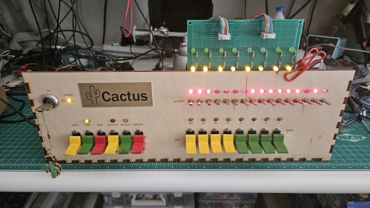
Both the Cactus (the original wooden prototype from years ago) and the new PCB Cactus(es) are essentially derived from a minimal 6502 computer design by Grant Searle for their core logic. Here's what that would look like on a breadboard:
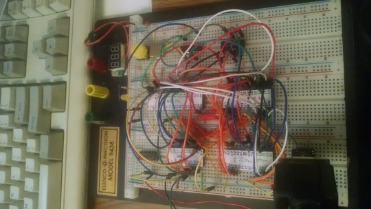
There isn't much to it, it's 32K of RAM, 16K of ROM containing Ohio Scientific's version of Microsoft BASIC, a 6850 ACIA for serial interaction, some logic gates, and of course a 6502 microprocessor (NMOS or CMOS, doesn't matter which). You hook it into a terminal and away you go.
Grant's design in turn can be best described as a distilled, modernized version of the OSI Challenger series of computers. Here's an OSI-400 and a Challenger 4P respectively:

The left one is a replica of the 400 circa 1976, also called the Superboard. It was affordable, endlessly reconfigurable and hackable, but ultimately very limited in capabilities. No BASIC, minimal monitor ROM you talk to over serial, but you could connect it to a bus to augment its features and turn it into a more powerful computer.
Whereas the OSI C4P on the right from about 1979 has more RAM, a video card, keyboard, BASIC built in, serial interface, cassette tape storage, and that's just the standard configuration. There was more room to expand and augment it to your needs inside the chassis (alot changed in 3 years for home computer users).
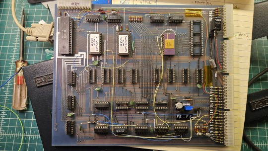
Grant's minimal 6502 design running OSI BASIC is a good starter project for hobbyists. I learned about the 6502's memory map decoding from his design. I modified and implemented his design on a separate cards that could connect to a larger backplane.
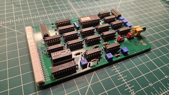
Here are the serial, ROM, RAM, and CPU cards respectively:
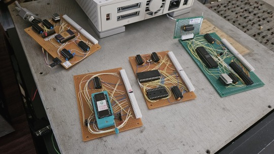
Each one is 100% custom, containing many modifications and fixes as I developed the design. However, that's only half of the computer.
I really wanted a 6502 machine with a front panel. People told me "nobody did that", or couldn't think of examples from the 1970s but that seemed really strange to me. Especially since I had evidence to the contrary in the form of the OSI-300:
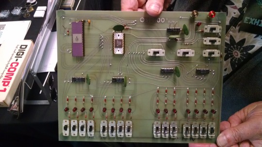
This one I saw at VCF West back in 2018 illustrates just how limited of a design it is. 128 bytes of RAM, no ROM, no serial -- just you, the CPU, and toggle switches and LEDs to learn the CPU. I was inspired the first time I saw one in 2015 at VCF East, which is probably when this whole project got set in motion.
Later that year I bought a kit for a miniature replica OSI-300 made by Christopher Bachman, and learned really quickly how limited the design philosophy for this particular front panel was. It was a major pain in the ass to use (to be clear, that's by OSI's choice, not any fault of Christopher in his implementation)

So... I designed my own. Took awhile, but that's the core of what the Cactus is: my attempt at experiencing the 1970s homebrew scene by building the computer I would have wanted at the time. Over half of the logic in the Cactus is just to run the front panel's state machine, so you can examine and modify the contents of memory without bothering the 6502. I added in all of the things I liked from more advanced front panels I had encountered, and designed it to my liking.
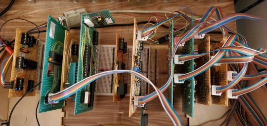
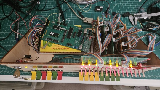
Here's the original front panel, accompanying logic, and backplane connected to the modern single board computer (SBC) version of the machine:
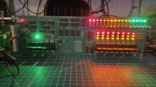
And here's the new Cactus SBC working with the new front panel PCB, which combines the logic, physical switch mountings, and cabling harnesses into a single printed circuit board.
So, what can you do with it? Pretty much the same things I do already with other contemporary 1970s computers: play around in BASIC, fire up the occasional game, and tinker with it.
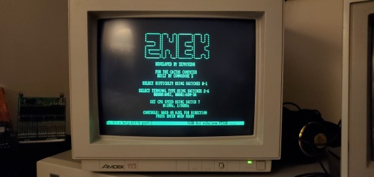
I've got no permanent storage designed for the Cactus as yet, it's been one of those "eventually" things. The good news is that a variety of software can be ported to the hardware without too much trouble for an experienced hobbyist. A friend of mine wrote a game called ZNEK in 6502 assembly which runs from a terminal:
Right now, you have to either toggle in machine programs from the front panel from scratch, burn a custom ROM, or connect it to a serial terminal to gain access to its more advanced features:

Here's it booted into OSI BASIC, but I have also added in a modern descendant of Steve Wozniak's WOZMON software for when I need to do lower level debugging.
I've also got a video card now, based on the OSI-440. I have yet to implement a keyboard, or modify BASIC to use the video board instead of the serial connection. Even if I did, screen resolution is pretty limited at 24x24 characters on screen at once. Still, I'm working on that...

Anyway, I hope that answers your question. Check the tags below to see the whole process stretching back to 2017 if you're curious to learn more of the project's history. I'm also happy to answer any more questions you might have about the project.
267 notes
·
View notes
Text
A controller with a scroll wheel, you say?
Well this is a little funny. Yesterday I posted the first part of a series of post on the fine details of how computers work, mentioning how I've been looking into this as part of a personal project I've been working on, and today I wake up to see Masahiro Sakurai posting a youtube video lamenting the lack of... this exact thing I'm working on.
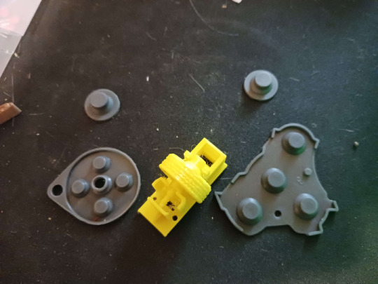
Apologies for how much cat hair is in this photo, that's a bit of an occupational hazard, but this here is a photo I took back in September when most of the parts I had to order were in for the prototyping of this thing:
That's a really bad MS Paint mockup, but yeah. I'm designing my own game console, and one of the key features is a big ol' scroll wheel right in the center of the controller. Another is that I'm planning to just put all the designs of the circuit boards and 3D printer files for the casing/buttons up online for free, making it this totally open DIY thing where anyone who's a big enough nerd can just make a couple downloads, order some dirt cheap components, and build their own copy of the system (or people with better setups than me can build and sell them, whatever). So I'm not super worried about anyone stealing my ideas or whatever, but I WOULD like to establish a standard and all that, and figured it was worth noting that this is something I've been slowly working towards for like a year or two now, and didn't just get the idea from this video:
youtube
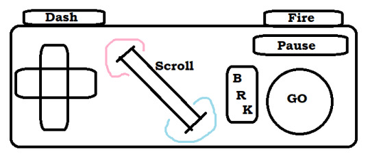
But yeah, now that the idea's out in the public consciousness, here's the plan for the controller (that I was planning to keep under my hat until I had a working prototype and some demo software sometime next year).
First off, the plan is that this is to be the standard controller for a whole console I'm also plucking away at designing, which is a bit more ambitious of a project, so I figure I might as well make it compatible with something that's already out there. So specifically, I'm designing this so that you can take one, plug it right into an SNES (or with a different connector at the end, an NES, because turns out they use the exact same input handling standard and it's just the shape of the plastic on the end that differs), and have it just work. Or mostly work anyway. I'm hoping I can process a signal out of the scroll wheel in a way that it either just needs the 3 extra bits of the input signal I don't have buttons for in my design (more on that later) or failing that, I can get it to output the same sort of signal as one wheel in the SNES mouse, which just rides along the second data line very few things use. I think that plan might break multitap compatibility and require an extra chip on the controller PCB, but it would leave this slightly more compatible with existing games on the same hardware. I might also do something weird with the button mapping to be sure NES select is on a shoulder and it works right out of the box with that whole library.
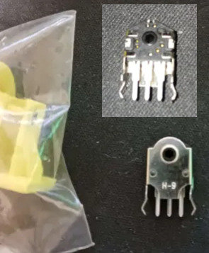
Working out exactly how to handle signals from the scroll wheel happens to be the point I'm currently stuck on by the way. I got this baggie full of rotary encoders for just a few cents which... almost fit in my first draft 3D printed wheel housing, but I have NO documentation on them, not even a part number/manufacturer besides "H-9," the pins don't fit a breadboard, and I've kinda been scrambling for rent so I can't afford a nice multimeter or oscilloscope to poke around with. Plus again I need to redesign this wheel print to even get it to spin right, and... this was a gift from a friend with a printer who is Not Local. Solvable problem, just needs more time and/or outside expertise.
But yeah, once I have those kinks worked out, it should be easy enough to get a custom board design made, replicas of end-cap of the controller cord are another problem easily solved by ordering a 1 dollar part or 3D printing something. The actual cord might be tricky since I don't know where you actually order something like that from, but it should be easy enough for anyone who doesn't mind a little assembly work to put one of these together and have it good to go for any software made with it in mind, or retrogames where you don't mind a weird button count. So... what's the pitch on this scroll wheel anyway?
Well for starters, there's the stuff Sakurai got into this morning. Any sort of RPG or text heavy game can use it to quickly scroll through menu options, or stuff in a text-heavy game. You could also pan the screen with it, something a lot of early 16-bit games assigned to the shoulder buttons or holding up and down while getting used to the new options the hardware was giving them.
Past that, you'll notice in my design it's at a 45 degree angle. I might have to tweak it a little, but my thinking is for a game that uses it heavily, one thumb or the other can slide over easily enough (I'm going for a pretty compact overall design) so we can have some games where you take your thumb off the D-pad, and have this nice analogue steering wheel. Nice for fine control in a racing game, or if you want some little radio-tuning/safe-cracking sorta deal.
Alternatively, move your right thumb over, use the D-pad to steer, shoot and dodge or whatever with shoulder buttons, and use the wheel to rotate a turret for a twin-stick sort of game maybe.
Or just use it for the sort of stuff mouse based games stick on the scrollwheel. Changing weapons, changing powerups... I'm planning to officially label the directions "hot" and "cold" to encourage weird gimmicky things like... I dunno, a platformer where you have a thermostat in your controller you can always mess with, freeze water coming out of pipes, crank up flame jets? Have a shot charging mechanic where you just really crank it to get to max strength? Weird minigame stuff. There's some fun space to explore with it.
Then we have the rest of the design here... which basically comes down to me being just plain sick of how every controller made by anyone in the past... 20 years give or take has kind of the exact same layout? 4 good face buttons, a D-pad, 4 shoulder buttons, 2 sticks, and 1-4 annoying to reach tiny awkward middle buttons, and we're just kind of overdue for a change-up?
Like first of all, hey, this is just too many buttons. There's a ton of games that really only need a D-pad, and maybe 3 buttons (attack jump pause) and the two things that aren't fully standardized is how awkwardly placed the D-pad is and how awful and awkwardly placed the pause button is. Shoulder buttons can be nice, but I've never really felt like 4 of them awkwardly crammed on the rim has been really useful or ergonomic, and that's coming from someone who's been playing a ton of FF14, which gets more use out of them than anything else I could name. And really, aside from games doing fake twin-stick stuff and using the whole grid like a second D-pad, I'm having a really hard time thinking of any game I've ever played that really makes good use of 4 good face buttons? Like people will use them if they've got'em sure, but unless you do that keyboard style thing where you lay the controller on a table and use all your fingers, you can really only comfortably hit 2 face buttons without sliding your thumb away from them, maybe comfortably make a quick pivot to a third.
Also, really, a lot of designers just sort of feel compelled to map SOMETHING to every button, even if it's clear the design didn't really need them. So basically I figure I'll try kinda just taking a "less is more" approach here. Here's the buttons that it's comfortable to rest your thumbs and fingers on, here's a dedicated pause/menu button where people often stick a kind of redundant menu button, here's my gimmicky scrollwheel. That's it, work around that.
I'm also going a little Gamecube inspired (literally using replacement membranes for one in my prototype design, even). Gonna make a great big primary button and use different shapes for the other two. Trying to label these in a less arbitrary fashion than most. If shooting a gun is a thing you do in this game, and there isn't a real good reason not to, default it to this nice right trigger you can hold down all the time. If we're advancing through menus or jumping or holding down gas in a car, here's the big GO button. Need brakes, need to break stuff with a melee attack? Go back in a menu system? There's your other face button. Have a quick dash move or a run you hold down, let's just use the other shoulder.
So yeah. That's my controller. Need to work out the kinks on the scroll wheel, source a cord, and hopefully I can slap things together and this will be something you can just order bits for piecemeal and put together for like, $5-10 after shipping? Maybe less? The parts are shockingly cheap so far.
But yeah if anyone has any insight to the scroll wheel or cord issues, let me know. Also the whole thing is presently a tad back-burnered because I am in a serious financial crisis and I don't want to have electronics spread all over my table if I have to abruptly find a new place to live if I can't scrape next month's rent together. So as usual, donations are incredibly welcome.
2 notes
·
View notes
Text
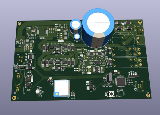
Let me introduce my current main WIP. It's not fandom related, it's for my model railroad, and it's not yet finished.
This is a rendering of a circuit board that I'm designing at the moment. It will be a DCC command station. My model railroad is run digitally, which means the tracks carry digital signals that tell each locomotive and switch individually how to run, which lights to turn and so on. The command station is the device that generates that. I have a number of different layouts, one of which has a good command station, one of which has a crappy old one, and the final one isn't even digital yet. So this will be the one that solves all issues for me, hopefully.
The design above isn't finished yet, and even the parts that are are not yet fully representative. The different capacitors are just there as options; some screen print overlaps; and some components (in particular all plugs and the relays that control the programming track) don't have 3D models so they don't show up.
Planned features:
Four layer board
10-25 V DC output, software controllable
Up to 5A output power, limited mainly by the main switching regulator.
Input 15-25V either AC or DC with polarity protection, selectable with some solder bridges (not yet in there). Optionally you can also bypass the main power regulator with another solder bridge (that I haven't added yet); useful in case you use e.g. a laptop power supply with a switchable voltage and don't need any regulation after that.
Railcom support
USB connection; not yet sure what for, but the main chip I'm using has USB support and I have some spare USB connectors here, so in it goes.
Speaking: The chip is an STM32L433RCT6P, chosen because I found it in stock at an electronics distributor. 64 kB RAM, 256 kB EEPROM, with support for an additional up to 256 MB externally (there's a spot for that on the board) and lots of fun extras that I don't technically need. It has an FPU! I don't need an FPU, but I will definitely do some floating point math computation on it just for fun.
Main external connection is WLAN using an ESP32 WROOM U module. I haven't decided on the housing, but I may go for extruded aluminum, so it's the U version that allows and requires an external antenna
It supports XBUS/XpressNet connections for old throttles from Lenz and Roco that I should probably throw away, but I paid good money for them, dang it.
It supports CAN for LCC / OpenLCB. I may not populate this part on all boards that I'm building, because I haven't actually decided whether I am interested. But the chip has CAN functionality built in, so why not.
There's an I2C connection to connect a cheap tiny OLED display for status messages.
Test points for all important signals (in particular the different internal voltage levels; yes, there is 3.3V, A3.3V and -3.3V and I need all of them).
Stuff still to add:
I will add pin headers (or space for pin headers anyway) for all the remaining pins on the STM32, and perhaps some on the ESP32, for future expansions.
Status LED and stop/go button on the front
Wire it all up, maybe move some stuff (mostly the STM32 around), which will cause all sorts of fun new routing issues.
Adjustments to make the jacks line up with the front panel once I've decided on a housing.
Features I'm not considering adding:
s88. I vaguely know what it is but I don't have any devices like that, and if that ever changed I could probably build (or perhaps buy) a converter that connects them via CAN.
Other buses like LocoNet.
Ethernet. I don't need it and it's actually more expensive than WLAN in this day and age.
In terms of software, I'm planning to use DCC-Ex on it. The whole project actually started out as a DCC-Ex shield, but once I realised that this wouldn't fit, I decided to make it standalone. Now, DCC-Ex is designed for Arduino, not STM32, and it doesn't support XpressNet, nor OpenLCB, nor Railcom, and their Wifi protocol is pretty weird and annoying which will be an issue (I'm planning to write my own control app for iPhone for it), so I'll probably change that or just replace it with the z21 one… so really, the software will not look a lot like DCC-Ex once I'm done with it.
Will this all work? I have honestly no idea. I mean, I'm fairly confident, I'd have given up on this long ago otherwise, but I have no guarantees either way until I've spent a lot of money on components and circuit boards and start soldering. Turns out doing it this way is not really cheaper than just buying a half-way decent one. That's what makes it exciting, though!
If it does work, obviously this will be released as open source. But it's still going to be a few days (more realistically weeks) before it's even ready to order the parts, and then a lot of soldering (current BOM stands at 194 actual components), and then a lot of software development before it's ready for that.
5 notes
·
View notes
Text
The Art and Science of PCB Reverse Engineering: A Comprehensive Guide
In the world of electronics, understanding how a printed circuit board (PCB) works can be crucial for troubleshooting, innovation, and learning. PCB reverse engineering is a process that allows engineers, hobbyists, and researchers to dissect and comprehend the intricate designs of existing PCBs. Whether you're looking to replicate an old design, learn about advanced technologies, or modify existing hardware, PCB reverse engineering offers valuable insights and opportunities. In this blog post, we’ll explore the essentials of PCB reverse engineering, its benefits, and practical tips for getting started.
What is PCB Reverse Engineering?
PCB reverse engineering is the process of analyzing and deconstructing a PCB to understand its layout, design, and functionality. This typically involves examining the physical board and its components to recreate or modify the circuit’s schematic diagram and design files. The goal is to uncover the design details that are not readily available from the manufacturer, enabling you to replicate or improve the existing design.
Why Engage in PCB Reverse Engineering?
Learning and Education: For students and hobbyists, reverse engineering provides a hands-on way to learn about electronic circuit design, component functions, and board layout. It’s a practical method to understand how various components interact within a circuit.

Repair and Maintenance: When dealing with older or discontinued hardware, PCB reverse engineering can help in diagnosing faults and replacing faulty parts. This is particularly useful for repairing vintage electronics where original schematics are no longer available.
Innovation and Design: Engineers often use reverse engineering to analyze competitor products, understand their design choices, and find areas for improvement. By learning from existing designs, they can innovate and create better, more efficient products.
Legacy Support: Companies maintaining legacy systems may need to reverse engineer PCBs to continue providing support, upgrades, or replacements for outdated technology.
The PCB Reverse Engineering Process
Reverse engineering a PCB involves several steps, each requiring precision and careful analysis. Here’s a simplified overview of the process:
Disassemble the PCB
Carefully remove the PCB from its enclosure or casing. Use tools like tweezers and anti-static mats to handle the board and avoid damaging sensitive components.
Document the Board
Take high-resolution photographs of both the top and bottom layers of the PCB. These images will serve as reference material during the reverse engineering process. Ensure that the images are clear and well-lit.
Identify Components
Label and identify all components on the PCB. This includes resistors, capacitors, integrated circuits (ICs), and connectors. Use a multi meter or component tester to help identify and measure components if necessary.
Trace the Circuit
Use the photographs to trace the circuit connections. This involves mapping out the paths of electrical connections between components. Tools like PCB design software can assist in recreating the circuit schematic.
Create the Schematic Diagram
Based on your tracing, create a schematic diagram that represents the electrical design of the PCB. This step is crucial for understanding how the circuit functions and for making any modifications.
Design the PCB Layout
Once the schematic is complete, design a PCB layout that matches the original design. PCB design software can be used to create and refine the layout, ensuring that it accurately reflects the original board’s design.
Verify and Test
Before finalizing the design, verify that the recreated PCB functions as intended. Build a prototype and test it to ensure that it meets the required specifications and performs correctly.
PCB reverse engineering is a powerful technique for understanding and working with electronic circuits. Whether you’re aiming to repair vintage hardware, learn about circuit design, or innovate in the field of electronics, mastering the art of PCB reverse engineering can provide significant advantages. By following the steps outlined in this guide and utilizing the right tools, you can delve into the intricate world of PCB design and uncover the secrets behind your favorite electronic devices.
0 notes
Text
0 notes
Text
Understanding Special PCB: The Backbone of Customized Electronics
In today’s rapidly evolving technology landscape, Special PCBs (Printed Circuit Boards) have become a cornerstone in customized electronics, playing a pivotal role in industries like aerospace, healthcare, telecommunications, and automotive. These specialized boards are tailored to meet unique design requirements and performance standards that exceed conventional PCB capabilities.

What are Special PCBs?
Special PCBs are distinct from standard circuit boards due to their specific materials, layout designs, and intended applications. These boards are used for devices that operate in harsh environments, require higher performance, or need to be compact and efficient. Whether it’s rigid-flex PCBs, aluminum-based PCBs for LED lighting, or multilayer boards, special PCBs are designed to cater to niche market needs.
The Role of PCB Manufacturing in Special PCBs
Creating special PCBs demands cutting-edge PCB manufacturing processes and advanced technology. The production of these PCBs involves multiple stages, including:
Design and Prototyping: Advanced software is used to design the layout, followed by the creation of prototypes for testing.
Material Selection: Special materials, such as ceramic, polyimide, or copper-clad laminates, are chosen based on the application’s specific needs.
Precision Assembly: The manufacturing of special PCBs requires high-precision assembly techniques like surface mount technology (SMT) and through-hole assembly to ensure reliability and performance.
PCB Board Makers: Experts in Customization
Leading PCB board makers like Shenzhen Shuoqiang Electronics (SQPCB) specialize in delivering high-quality special PCBs tailored to individual specifications. With state-of-the-art manufacturing facilities, SQPCB can handle small-scale prototype projects or large-scale production orders, ensuring precision, durability, and performance.
Assembly of Special PCBs
PCB manufacturing assembly is a critical phase where components are mounted onto the PCB substrate. For special PCBs, the assembly process requires meticulous attention to detail due to their complexity. Whether it’s high-density interconnect (HDI) boards or PCBs with intricate multilayer designs, the right assembly process ensures the optimal functionality of the circuit.
The PCB assembly process typically involves:
Soldering Components: High-quality soldering methods, like reflow soldering, are used to attach components to the board accurately.
Testing and Quality Control: After assembly, PCBs undergo rigorous testing to ensure they meet quality standards and perform as intended in their specific applications.
Why Choose SQPCB for Special PCB Manufacturing?
SQPCB stands out as a trusted PCB board maker for several reasons:
Customization: Their team of experts works closely with clients to deliver customized special PCBs tailored to specific requirements.
Advanced Technology: They use the latest tools and technologies to ensure the highest standards of manufacturing and assembly.
Quality Assurance: With a robust quality control process, every PCB manufactured by SQPCB is rigorously tested to ensure reliability and performance.
Competitive Pricing: SQPCB offers cost-effective solutions without compromising on quality, making them a preferred partner for businesses of all sizes.
Conclusion
Special PCBs are critical in driving innovation in various sectors, offering unmatched performance and adaptability for custom electronic devices. By partnering with experienced PCB board makers like SQPCB for PCB manufacturing and assembly, businesses can ensure the production of high-quality, reliable, and efficient special PCBs for their unique applications.
#Special PCB#pcb manufacturing#customize pcb#flex pcb#pcb manufacturers#multilayer pcb#advertising#rigid flex pcb#business
0 notes
Text
Printed Circuit Board (PCB): The Backbone of Modern Electronics
A Printed Circuit Board (PCB) is an essential component in nearly all electronic devices. These boards are designed to mechanically support and electrically connect various electronic components using conductive pathways. The significance of PCBs in today’s technological landscape cannot be overstated, as they form the foundation upon which most modern electronics are built. Whether it's a smartphone, computer, or even complex industrial equipment, the PCB plays a crucial role in their functionality.
Structure and Components of a PCB
At its core, a PCB is made up of a non-conductive substrate material, typically fiberglass or composite epoxy, with conductive copper traces embedded on it. These traces form electrical circuits that allow components such as resistors, capacitors, transistors, and integrated circuits to communicate and work together. The components are mounted onto the board through a process called soldering, where a metallic substance binds them to the copper pads, ensuring strong electrical connections.
There are several layers in a typical PCB:
1. Substrate Layer: The base material, often fiberglass, provides rigidity and insulation.
2. Copper Layer: A thin copper foil is laminated onto the substrate, forming the conductive pathways.
3. Solder Mask Layer: This is a protective layer that covers the copper traces, preventing short circuits and oxidation.
4. Silkscreen Layer: Used for printing labels and markings, this layer helps technicians and engineers identify components on the board.
PCBs can range from simple single-layer boards to more complex multi-layer boards. In advanced applications, multi-layer boards are used, where multiple copper layers are sandwiched together with insulating layers between them. This allows for higher component density and more complex circuitry in a compact form factor.
Types of Printed Circuit Boards
PCBs come in several different types based on the complexity of the design and the needs of the application:
1. Single-Sided PCB: The simplest form, with components and copper traces on one side of the substrate.
2. Double-Sided PCB: These boards have components and copper traces on both sides of the substrate, offering more flexibility for routing electrical connections.
3. Multi-Layer PCB: As the name suggests, these boards have multiple layers of copper traces, making them ideal for complex and high-performance applications.
4. Rigid PCB: These are made from solid, inflexible materials, commonly used in devices where the board must maintain a specific shape.
5. Flexible PCB: These boards are made from flexible materials and can bend, fold, or twist. They are often used in compact devices where space is limited.
6. Rigid-Flex PCB: A hybrid of rigid and flexible PCBs, these are used in complex devices that require both flexibility and stability in specific areas.
Manufacturing Process
The manufacturing of a PCB involves several precise steps to ensure quality and reliability:
1. Design: The process begins with creating a design using PCB design software. This includes defining the layout, trace routing, and component placement.
2. Printing the Design: Once the design is finalized, it is printed onto the copper-clad substrate using a photomask or a direct laser printing method.
3. Etching: Any excess copper is removed from the board, leaving only the desired copper traces.
4. Drilling and Plating: Holes are drilled where components will be placed, and conductive materials are plated inside these holes to establish connections between layers in multi-layer boards.
5. Solder Mask Application: A solder mask is applied to protect the copper traces and prevent short circuits.
6. Silkscreen Printing: Component labels and identification markers are printed onto the board.
7. Testing and Quality Control: The finished PCB undergoes rigorous testing to ensure there are no defects in the circuitry or connections.
Applications of PCBs
PCBs are found in a vast array of electronic devices and systems. Some of the key application areas include:
Consumer Electronics: Smartphones, tablets, computers, and home appliances rely heavily on PCBs for their operation.
Automotive Industry: Modern vehicles contain numerous electronic systems, from engine control units to infotainment systems, all powered by PCBs.
Medical Devices: Precision medical equipment like diagnostic machines and wearable health devices depend on reliable PCBs for accurate functionality.
Telecommunications: Communication devices, including routers, switches, and mobile towers, are equipped with PCBs that handle data processing and signal transmission.
Aerospace and Defense: In high-stakes industries like aerospace and defense, robust PCBs are required for mission-critical systems, including avionics and radar equipment.
Future Trends in PCB Technology
As technology continues to evolve, so too does the development of PCBs. Advances in materials science, miniaturization, and automation are paving the way for even smaller and more powerful PCBs. Innovations such as flexible hybrid electronics (FHE), 3D-printed circuits, and high-speed PCB designs are expected to revolutionize industries by enabling more compact, lightweight, and efficient electronic devices.
Moreover, with the rise of the Internet of Things (IoT) and 5G technology, the demand for high-performance PCBs capable of handling greater data transmission speeds and power efficiency is surging. This trend will likely lead to more widespread use of multi-layer and flexible PCBs in upcoming technological advancements.
Conclusion
The printed circuit board is undeniably one of the most vital components in modern electronics. Its evolution has allowed for remarkable advancements in technology, from the devices we use daily to the complex systems that run industries. As innovations in materials and design continue, PCBs will remain at the forefront of the ever-expanding world of electronics, enabling new possibilities and driving the next wave of technological breakthroughs.
1 note
·
View note
Text
How to Choose the Best PCB Design Tool for Your Project
Printed Circuit Board (PCB) design tools are crucial for electronic engineers and designers. They facilitate the creation, modification, and validation of circuit boards, making the design process efficient and error-free. However, selecting the right PCB design tools is challenging, given the wide variety of options available in the market. This article will guide you through the factors to consider when choosing the best PCB design tool for your project, ensuring you make an informed decision that meets your needs.
Choosing The Best PCB Design Tool for Your Project
Understand Your Project Requirements
The first step in selecting a PCB design tool is to evaluate the specific needs of your project. Not all tools offer the same features, so understanding your project's demands is crucial.
- Complexity: Is your design simple with a single-layer PCB, or does it involve multiple layers with complex circuits?
- Type of Components: Are you working with analogue, digital, or mixed-signal designs? Some tools specialize in one or the other.
- Size of the Project: How many components are involved, and how large will your PCB be? If you are working on large-scale projects, you’ll need software that supports complex designs.
Ease of Use
The learning curve of PCB design software can vary significantly. If you are a beginner, look for user-friendly tools with intuitive interfaces. On the other hand, if you are an experienced engineer, more advanced features might be a priority, even if they come with a steeper learning curve.
- Interface Design: A well-designed interface with easy-to-navigate menus, drag-and-drop functionality, and visual aids like real-time 3D previews can significantly improve your workflow.
- Tutorials and Documentation: Ensure that the software you choose offers comprehensive tutorials, user guides, and forums to help you understand the tool’s functionality. This is particularly important if you are new to PCB design.
Key Features to Look For
Modern PCB design tools come with a variety of features. Here's what you should prioritize:
- Schematic Capture: A good PCB design tool should have an efficient schematic capture feature, allowing you to create and modify circuit diagrams before starting the actual PCB layout.
- Layout Editor: Look for software that includes a powerful layout editor. Features like routing automation, design rule checking (DRC), and constraint management are essential.
- Component Library: An extensive, customizable component library is vital for streamlining the design process. Some tools allow you to import new components, saving time and effort.
- 3D Visualization: Many modern PCB design tools offer 3D views of your design, enabling you to inspect the layout from different angles and catch potential errors early in the process.
- DRC and ERC (Electrical Rule Check): Design Rule Checking ensures that your PCB adheres to manufacturing requirements, while Electrical Rule Checking ensures that your circuits are functional and error-free. Both features are must-haves for any severe PCB designer.
- Auto-Routing: This feature automatically connects all your components based on the schematic. While manual routing offers more control, auto-routing can save significant time on less critical areas of the design.
Compatibility and Integration
When selecting a PCB design tool, consider how well it integrates with other software and hardware you are using:
- File Format Compatibility: Ensure the software supports standard formats like Gerber, DXF, or ODB++. This ensures that you can easily export and share your designs with manufacturers.
- Integration with Simulation Tools: If you are working with circuit simulations (e.g., SPICE), check if the design tool supports simulation integration. This allows you to simulate the behaviour of your circuits before committing to a final design.
- Collaboration Features: If your project involves teamwork, look for tools that offer collaboration features, such as version control, shared libraries, and cloud-based storage.
Cost and Licensing Options
Budget is another critical factor to consider when choosing a PCB design tool. Both free and paid options are available, and the cost typically reflects the functionality and complexity of the tool.
- Free Tools: If you're working on a small project or learning PCB design, free tools like KiCAD, EasyEDA, and Fritzing may be sufficient. However, these may lack advanced features like multi-layer design, auto-routing, and extensive component libraries.
- Paid Tools: For professional projects, consider investing in paid software like Altium Designer, OrCAD, or Eagle. While these tools come with higher price tags, they offer advanced features, better support, and regular updates.
- Subscription vs. One-Time Purchase: Some PCB design tools operate on a subscription model, while others require a one-time purchase. Evaluate which model makes sense for your project and your long-term needs.
Platform Compatibility
Ensure that the software you choose is compatible with your operating system. Most PCB design tools are compatible with Windows, but not all support macOS or Linux. Check if the software has a web-based version, which could offer cross-platform flexibility without installation.
Community and Support
Access to an active user community and technical support can make a significant difference, especially when facing a complex design problem.
- User Forums and Online Communities: Active forums or user groups can be a goldmine for troubleshooting, sharing design tips, and exploring advanced features.
- Technical Support: Look for software providers that offer robust customer support, including live chat, email support, or even personalized training sessions. This is particularly important for professional projects where deadlines matter.
Manufacturer Compatibility
Before finalizing a PCB design tool, consider the manufacturer's compatibility. Some PCB design tools have built-in integrations with specific manufacturers, allowing you to upload your designs for prototyping and production directly. This feature can save you time and reduce the chances of errors during manufacturing.
Future Scalability
While your current project may be small or mid-sized, it's worth considering whether your chosen tool can scale with your future needs. If you plan to work on more complex, high-layer, or multi-board designs, you’ll want software that can handle the additional complexity without requiring you to switch platforms.
Top PCB Design Tools to Consider
Here’s a quick overview of some of the top PCB design tools based on the factors discussed above:
- Altium Designer
- Best For Professionals working on complex, multi-layer designs.
- Key Features: Advanced schematic capture, PCB layout, 3D visualization, and collaboration features.
- Price: Paid, premium option.
- Eagle (by Autodesk)
- Best For Small to medium-sized projects with a focus on flexibility.
- Key Features: Schematic editor, auto-routing, comprehensive component library.
- Price: A free version is available, but paid plans offer more features.
- KiCAD
- Best For: Open-source enthusiasts or those working on small projects.
- Key Features: Multi-layer design, extensive component libraries, schematic capture.
- Price: Free.
- OrCAD
- Best For: Large, enterprise-level projects.
- Key Features: Advanced simulation, schematic capture, high-speed PCB design.
- Price: Paid, with a focus on enterprise users.
- EasyEDA
- Best For: Beginners and hobbyists.
- Key Features: Web-based tool with integrated PCB manufacturing options.
- Price: Free with paid manufacturing options.
Conclusion
Choosing the best PCB design tool for your project depends on several factors, including complexity, ease of use, features, and budget. By carefully evaluating your requirements and the features of available tools, you can find the one that best fits your needs and ensures a smooth and efficient design process. Whether you’re a hobbyist or a professional, the right PCB design software will significantly affect your workflow and the quality of your final product.
Read the full article
0 notes
Text
Find the best PCB manufacturing companies in Gujarat
Gujarat has also become the most suitable location for the manufacturing of PCBs owing to its rapid industrial development and utmost infrastructural facilities. The state has a solid industrial nature, and the government encourages further development by providing stimulus for electronics and PCB manufacturing. This makes it easy for the PCB manufacturing companies in Gujarat to find a suitable environment to operate from. These PCB manufacturing companies have highly developed technologically enabled capabilities and expertise in Gujarat.

Top PCB Manufacturing Companies in Gujarat
Epsilon Electronics
Epsilon Electronics is one of the leading PCB Manufacturing companies in Gujarat, operating in the fields of embedded systems and product engineering in India. From embedded software development services to industrial products and projects development, PCB manufacturing, and 3D design printing, Epsilon Electronics can be categorized as a one-stop-shop. The company has earned a reputation for quickly translating ideas into practicable solutions, which has led businesses to consider it as their preferred provider as PCB manufacturing companies in Gujarat.
The strengths that help Epsilon Electronics stand out from the other competitors are its sophistication in its tools and people to do the job. Their skills in quickly translating concepts into deliverables and their excellent customer relations make them a valued supplier in the PCB manufacturing sector. For specific requirements or for faster deliveries, Epsilon Electronics has the experience and capability that clients require when dealing with this company.
SB Electronics
SB Electronics is one of the pioneer organizations in PCB manufacturing companies in Gujarat having experience in this sector more than 25 years. The company deals in manufacturing multi-layer PCBs such as Single Side, Double Side P. T. H. (through-hole plating) and Double Side NON- PTH PCBs using high-end materials such as FR2, FR4, CEM. SB Electronics has always been committed to providing quality and innovative printed circuit boards making it a reliable supplier to diverse industries.
Using the information provided above, you can make a list of the best companies for pcb manufacturing in Gujarat for your next electronic project. For more details or to discuss your specific case, please do not hesitate to contact Epsilon Electronics. We are here to assist you in achieving your goal of having the finest PCB solutions in the industry. Click on the following link to visit our website now.
#PCB manufacturing companies in Gujarat#pcb manufacturing#pcb design company in india#PCB manufacturing companies#PCB manufacturing company#printed circuit board
0 notes
Text
Affordable PCB Design Services for High-Quality Prototypes
Looking for affordable PCB design services without compromising on quality? Bay Area Circuits offers expert solutions for high-quality PCB prototypes that meet your specific needs. Whether you're developing a simple single-layer board or a complex multi-layer design, our experienced team ensures precision and efficiency in every project.
Our services extend beyond just design. We provide printed circuit board fabrication, delivering fast, reliable, and cost-effective solutions. With cutting-edge equipment and years of experience, we create prototypes that meet industry standards, ensuring your product performs optimally from the start.
We also offer advanced printed circuit board design software like InstantDFM to streamline your design process. This tool allows you to check for manufacturability, reduce errors, and optimize your design, saving you time and money. InstantDFM provides automated feedback and pricing within minutes, ensuring a smooth transition from design to production.
Choose Bay Area Circuits for affordable PCB design services and high-quality prototypes. With our expertise, you can bring your electronic products to market faster and with confidence. Contact us today! To know more, Visit - https://bayareacircuits.com/
0 notes
Text
Leading Circuit Board Manufacturers in Canada: Precision and Innovation
Canada is home to a growing number of circuit board manufacturers in canada offering high-quality PCB solutions for a wide range of industries. These manufacturers specialize in producing advanced printed circuit boards (PCBs), including rigid, flexible, and metal-clad designs, serving sectors such as telecommunications, automotive, aerospace, and medical devices. Canadian PCB manufacturers are known for their commitment to precision, quality, and innovation, often providing customized solutions to meet specific client needs. With state-of-the-art facilities and a focus on sustainability, these companies help drive technological advancements while ensuring reliable performance in demanding environments. For more details visit our website www.crimpcircuits.com
#pcb manufacturing toronto#printed circuit board design#metal clad pcb#printed circuits#rigid flex pcb#full turnkey pcb services#turnkey pcb services#pcb parts#eagle software#pcb designing#flexible pcb#pcb assembly#printed circuit board manufacturers#pcb manufacturers in canada#circuit board manufacturers in canada#pcb quote#pcb prototype services in canada
0 notes
Text
PCB Clone Services: Precision in Reproduction
What is PCB Cloning?
PCB Clone is the process of creating an exact replica of an existing printed circuit board (PCB). This service is essential when you need to reproduce a board for which the original design files are unavailable. PCB cloning involves reverse engineering the board to generate the necessary data for manufacturing a duplicate.
The Role of PCB Clone Services
PCB Cloning Service are vital in scenarios where you need an identical copy of an electronic circuit board. Whether it’s for replacing obsolete hardware, producing additional units, or creating backups, these services ensure precision in reproduction.

How PCB Cloning Works
1. Initial Analysis
The cloning process begins with a detailed analysis of the original PCB. This includes examining the board’s layout, components, and circuitry. Engineers carefully inspect every detail to ensure accurate replication.
2. Reverse Engineering
After the initial analysis, the reverse engineering phase begins. Engineers trace the circuitry, identify components, and create a schematic of the board. This step is crucial in understanding how the PCB functions.
3. Schematic Capture and Layout Design
Once the reverse engineering is complete, a schematic diagram is created. This diagram serves as a blueprint for the new board. Engineers then use specialized software to design a PCB layout that matches the original.
4. Prototyping and Testing
Before full-scale production, a prototype of the cloned PCB is manufactured. This prototype undergoes rigorous testing to ensure it functions exactly like the original board. Any necessary adjustments are made during this phase.
5. Mass Production
Once the prototype passes all tests, the PCB is ready for mass production. The final product is an exact clone of the original board, ready for use in any application.
Benefits of PCB Cloning Services
• Obsolete Hardware Reproduction: Clone services are ideal for replicating outdated circuit boards, ensuring continued operation of legacy systems.
• Cost-Effective: Cloning is often more cost-effective than redesigning a PCB from scratch.
• Fast Turnaround: PCB cloning services can quickly produce duplicates, reducing downtime for critical systems.
Challenges in PCB Cloning
PCB cloning, while beneficial, is not without its challenges. Complex multilayer boards, proprietary components, and encrypted firmware can complicate the cloning process. Skilled engineers are essential to navigate these obstacles and deliver an accurate clone.
Choosing the Right PCB Clone Service
When selecting a Clone PCB Service, consider factors such as experience, technology, and the ability to handle complex projects. A reliable service provider will ensure that your cloned PCBs meet the highest standards of quality and performance.
Conclusion
PCB cloning services play a crucial role in the electronics industry. Whether for preserving legacy systems or producing additional units, these services provide a reliable solution for duplicating PCBs with precision. With the right expertise, PCB cloning ensures that your electronic systems continue to function smoothly, regardless of the challenges posed by outdated or unavailable designs.
0 notes
Text
PCB Manufacturing: A Comprehensive Exploration of Modern Assembly Services
In the electronics manufacturing sector, PCB (Printed Circuit Board) assembly services are indispensable. Numerous companies provide rapid prototyping and mid-volume production services tailored to the intricate demands of diverse industries. This article delves into the complexities of these services, highlighting the technological prowess and strategic advantages of opting for domestic assembly options.
Innovative Prototyping and Expedited Assembly Services
Organizations specializing in PCB assembly emphasize their capability to execute rapid turnaround projects, typically within 1 to 5 days. These offerings are designed to support even the most complex or specialized boards, accommodating projects of any scale. Additional services such as Bill of Materials (BOM) validation and preliminary Design for Manufacturability (DFM) analysis are frequently included at no extra charge, demonstrating a dedication to quality and customer satisfaction from the beginning of the manufacturing journey.
Advantages of Domestic Mid-Volume Production
For mid-volume production, domestic PCB assembly offers several benefits. It is particularly valuable when quick turnaround times are essential or when projects contain sensitive intellectual property. Utilizing domestic facilities is also beneficial when products are destined for governmental agencies, involve export-restricted information, or when volumes are too small to benefit economically from offshore production. This method ensures greater control over the manufacturing process, improved traceability, and enhanced client involvement.
Tailored PCB Assembly Services
Top manufacturers expand their service offerings beyond basic assembly to include comprehensive support services. These may encompass component sourcing, rework and repair services, functional testing, and X-ray inspections, as well as specialized treatments such as encapsulation, potting, and various coatings. These customized services ensure that every aspect of PCB assembly is efficiently handled, from initial prototyping through to the completion of the final order.
Gaining a Competitive Advantage in PCB Assembly
Manufacturers that lead in PCB assembly often present several competitive benefits:
Swift, 24-hour turnaround for quotes.
Custom software tools for BOM validation.
Detailed DFM feedback.
Flexible procurement options for either turnkey or consigned parts.
No minimum order quantity, supporting a variety of project scales.
Advanced assembly techniques, including microelectronics and flip chip technologies.
These manufacturers typically select strategic equipment and keep their client base limited, ensuring personalized service and meticulous attention to detail.
Ensuring Quality and Achieving Certifications
Quality assurance is a cornerstone in PCB assembly, critical for ensuring the reliability and performance of the final products. This sector employs a suite of sophisticated inspection and testing procedures that are essential for maintaining high quality standards. Techniques like Solder Paste Inspection (SPI) and Automated Optical Inspection (AOI) are employed to detect any potential defects early in the assembly process.
X-ray analysis is another pivotal technique used to examine the internal features of PCBs, ensuring that hidden joints and components are correctly placed and soldered. Additionally, a variety of functional testing methods are utilized to verify that each board performs according to its design specifications under different conditions. Adherence to these rigorous practices is essential for achieving certifications that testify to the reliability and quality of the products. These certifications are often required by clients in highly regulated industries, underscoring the necessity of stringent quality controls in PCB manufacturing.
The Evolving Landscape of PCB Manufacturing
The PCB manufacturing industry is constantly evolving, propelled by technological advancements and the growing need for precision and efficiency. As firms continue to innovate and broaden their service range, the importance of selecting a PCB assembly partner with extensive capabilities and a solid quality management system becomes increasingly evident.
For entities requiring professional PCB assembly services, it is recommended to collaborate with manufacturers that not only meet the technical requirements but also align with strategic business objectives. This alignment is essential for fostering long-term partnerships and succeeding in sophisticated electronics manufacturing endeavors.
In summary, PCB manufacturing includes a broad spectrum of services and capabilities. From rapid prototyping to specialized mid-volume production, the industry provides customized solutions to satisfy the varied needs of its customers. By utilizing cutting-edge technologies and focusing on quality and client service, leading PCB assemblers are ideally positioned to meet the dynamic requirements of contemporary electronic devices.
0 notes
Text
Elevate Your Imaging Capabilities: Integrating USB Global Shutter Cameras in Quality Control
Accuracy and speed of quality control procedures are vital in today's hectic manufacturing environments. Many sectors are using cutting-edge imaging technologies, such the USB Global Shutter Camera, to meet these expectations. Compared to conventional cameras, this cutting-edge technology has a number of important advantages, especially for dynamic and fast applications. This blog post will discuss how incorporating a USB global shutter camera can improve quality control procedures and how to take use of its advantages to increase precision and productivity.
What is a USB Global Shutter Camera?
A USB Global Shutter Camera is designed to capture high-speed motion with exceptional clarity and precision. Unlike rolling shutter cameras, which scan images line by line, global shutter cameras capture the entire image at once. This feature is crucial in quality control settings where fast-moving parts or high-speed production lines require accurate and clear imaging to identify defects or inconsistencies.
Advantages of USB Global Shutter Cameras in Quality Control
Enhanced Image Accuracy
The primary benefit of using a USB Global Shutter Camera is its ability to eliminate motion blur and distortions. In high-speed environments, this capability ensures that every detail is captured with precision, allowing for more accurate inspections and defect detection. This enhancement is particularly useful in industries such as electronics, automotive, and pharmaceuticals, where even minor defects can lead to significant issues.
Improved Processing Speed
Speed is another critical factor in quality control. The USB Global Shutter Camera allows for rapid image capture, enabling real-time processing and immediate feedback. This rapid processing capability helps streamline production lines, reduce downtime, and improve overall operational efficiency. By integrating such cameras into your quality control systems, you can ensure that any issues are promptly addressed, maintaining high standards and minimizing waste.
Versatile Application
The versatility of the USB Global Shutter Camera makes it suitable for a wide range of quality control applications. From inspecting printed circuit boards (PCBs) to analyzing packaging integrity, these cameras adapt to various inspection needs. Their high-resolution and global shutter features make them ideal for both detailed inspections and broad overviews. This flexibility means that manufacturers can deploy the same camera for multiple inspection tasks, simplifying equipment requirements and reducing costs.
Implementing USB Global Shutter Cameras in Your Quality Control System
Choosing the Right Camera
Selecting the appropriate USB Global Shutter Camera involves considering factors such as resolution, frame rate, and connectivity options. High-resolution cameras provide more detailed images, while higher frame rates are essential for capturing fast-moving objects. Connectivity options, such as USB 3.0, ensure that the camera integrates seamlessly with existing systems and facilitates quick data transfer.
Integration with Existing Systems
Integrating a USB Global Shutter Camera into your existing quality control system may require some adjustments to your current setup. It is important to ensure compatibility with your software and hardware to maximize the camera’s benefits. Many camera manufacturers offer support and guidance for this process, helping you to achieve a smooth transition and optimal performance.
Summary: Transforming Quality Control with USB Global Shutter Cameras
Incorporating a USB Global Shutter Camera into your quality control processes offers significant improvements in image accuracy, processing speed, and versatility. By providing clear, distortion-free images of high-speed processes, these cameras enable more precise inspections and efficient operations. Their adaptability to various applications further enhances their value, making them a valuable addition to any quality control system.
For more information on integrating USB Global Shutter Cameras into your quality control system and to explore the latest models, visit VADZO Imaging. Elevate your imaging capabilities and ensure the highest standards of quality in your production processes.
0 notes
Last Seen Blogs

starrfan203-blog
CartoonFreaks

ssn-2
Maybe


mercedes-benz-fans-blog
Création: 1926

solomanta
Șolomanță