#VHDL Synthesis
Explore tagged Tumblr posts
Visit Tumblr Blog
Explore Tumblr blogs with no restrictions, modern design and the best experience.
Last Seen Tumblr Blogs


Fun Fact
Forty percent of Tumblr users are between the ages of 18 to 25.
Text
youtube
VHDL Basics : New to VHDL - Try your first code today : Tutorial with Live Example
Are you New to VHDL coding - I will help you on your first code today. We are making a simple digital system where you give 2 inputs say Input A & Input B, and it will give you the output after doing logical AND. In short we are making, a logical AND Gate, digital system. I am assuming you already know what is Logical AND and how it function. so I am jumping straight to coding part. If you donot know what is logical AND, You can refer HDLDesignLab.blogspot.com This video is perfect for beginners who are new to VHDL. I will explain the basic concepts of VHDL in a clear and easy-to-understand way. By the end of this video, you will be able to: Write a simple VHDL program Simulate your VHDL program Synthesize and view the RTL Schematics I hope you enjoy this video! I hope you feel little confident to start writing a small digital system now. VHDL Support all basic Gate functions by default, for example AND gate which we just desinged and apart that you will have OR Gate, Not Gate, NAND Gate, NOR Gate, XOR Gate and XNOR gate. So if you feel little confident, try design your own digital system for all these basic digital Gates and test them by own. I wish you the best. Once you are done, please let me know from the comment section.
Subscribe to "Learn And Grow Community"
YouTube : https://www.youtube.com/@LearnAndGrowCommunity
LinkedIn Group : https://www.linkedin.com/groups/7478922/
Blog : https://LearnAndGrowCommunity.blogspot.com/
Facebook : https://www.facebook.com/JoinLearnAndGrowCommunity/
Twitter Handle : https://twitter.com/LNG_Community
DailyMotion : https://www.dailymotion.com/LearnAndGrowCommunity
Instagram Handle : https://www.instagram.com/LearnAndGrowCommunity/
Follow #LearnAndGrowCommunity
#VHDL#tutorial#vhdl for biginners#vhdl code#verilog#example#first code#simulation#design#vhdl synthesis#beginners#learn#learn and grow community#vhdl example#student#enginner#training#free#session#grow#career#Engineering#course#AND gate#test#hdl design#technical training#Youtube
1 note
·
View note
Text
Mastering the Future of Chip Design: Explore ASIC Training from Anywhere
The Rising Relevance of ASIC Design in the Semiconductor Industry
In today’s tech-driven world, Application-Specific Integrated Circuits (ASICs) play a pivotal role in shaping electronic innovations. From smartphones and medical devices to artificial intelligence and automotive electronics, ASICs are embedded in almost every aspect of modern technology. As industries evolve, the demand for engineers skilled in ASIC design continues to surge. This increasing demand has created a clear path for aspiring VLSI professionals to seek specialized training that aligns with industry needs.
Why Online ASIC Design Training is the Smart Choice
The convenience and flexibility of learning from home have led to the growing popularity of online asic design training programs. These virtual platforms provide comprehensive learning modules that allow learners to gain hands-on experience without the limitations of geographical boundaries. Whether someone is a recent engineering graduate or an industry professional looking to upskill, these online programs make it easier to access quality education at one's own pace. With the use of simulation tools, video lectures, and live project support, learners receive training that is practical, relevant, and industry-focused.
Essential Skills Gained Through ASIC Training
ASIC design is a multifaceted field that combines knowledge of digital electronics, hardware description languages, verification methodologies, and physical design principles. A well-structured training program ensures that learners become proficient in tools such as Verilog, VHDL, Synopsys, and Cadence. It also fosters a strong understanding of timing analysis, synthesis, and low-power design techniques. These are essential competencies for engineers working in semiconductor and VLSI companies.
Hyderabad – A Growing Hub for ASIC Training Excellence
Hyderabad has become a prominent location for VLSI and semiconductor training, offering access to some of the finest educational resources in India. Several online asic design training institutes in hyderabad have emerged as reliable options for those aiming to build a career in chip design. These institutes not only provide technical guidance but also offer placement support, industry interaction, and live project exposure. Hyderabad’s growing ecosystem of VLSI companies further boosts the scope for real-world learning and employment opportunities.
Conclusion: Finding the Right Training Path in a Digital World
To thrive in the evolving semiconductor industry, quality education in ASIC design is indispensable. Choosing the right training platform can make a lasting impact on a learner’s professional journey. That’s why institutes like Takshila Institute of VLSI Technologies have become trusted names for those looking to gain advanced skills in VLSI. With its industry-aligned curriculum and online accessibility, it bridges the gap between academic learning and professional excellence.
Whether opting for online asic design training or exploring online asic design training institutes in hyderabad, the goal remains the same: to master the art of designing the future’s most critical hardware components.
0 notes
Text
Mastering VLSI Design: The Path to a Promising Career in Semiconductor Industry
The Rising Demand for VLSI Professionals
The semiconductor industry is experiencing a dramatic shift, powered by the growing demand for smaller, faster, and more efficient chips in everything from smartphones to electric vehicles. Very-Large-Scale Integration (VLSI) design plays a critical role in this transformation, enabling the integration of millions of transistors onto a single chip. As technology continues to evolve, the need for skilled VLSI engineers is expanding at an unprecedented rate. This demand has opened up a world of opportunities for those interested in chip design and semiconductor engineering. Companies worldwide are investing in VLSI talent to maintain a competitive edge, making this an ideal time for students and professionals to build a career in the field. Whether it’s designing system-on-chip (SoC) solutions or optimizing embedded systems, VLSI experts are becoming increasingly vital to the tech ecosystem.
Understanding the Fundamentals of VLSI Design
VLSI design involves the process of creating integrated circuits by combining thousands or even millions of transistors into a single chip. This complex engineering task requires a deep understanding of electronic circuit design, semiconductor physics, and design tools like Verilog, SystemVerilog, and VHDL. The curriculum in most vlsi training institutes includes modules on front-end and back-end design, logic synthesis, timing analysis, and verification methods. The end goal is to produce high-performance chips that are also power-efficient and cost-effective. VLSI engineers must possess strong analytical skills, a deep interest in electronics, and a passion for solving real-world problems. As technology nodes continue to shrink from 7nm to 3nm and beyond, the challenges in VLSI design grow more complex—demanding not just theoretical knowledge but also hands-on experience in state-of-the-art tools and practices.
Exploring Career Opportunities in VLSI
A career in VLSI is not only intellectually rewarding but also financially lucrative. From design engineers to physical design experts and verification engineers, the job roles in this domain are diverse and highly specialized. Each position plays a crucial part in bringing a semiconductor product from concept to fabrication. What makes VLSI especially appealing is the steady demand from both startups and tech giants involved in AI, IoT, and 5G innovation. Particularly in India, the ecosystem around semiconductor design is growing, creating an urgent need for competent professionals. The rise of online vlsi training institutes in bangalore has made it easier for aspiring engineers to access high-quality education and training without geographical constraints. With remote learning tools, recorded sessions, and access to simulators, these platforms are revolutionizing how VLSI education is delivered, allowing learners to gain industry-relevant skills from the comfort of their homes.
Key Skills and Tools Every VLSI Engineer Should Learn
To thrive in the VLSI domain, aspiring engineers must master a combination of technical skills and practical tools. On the technical side, knowledge of digital electronics, CMOS design principles, and signal integrity is foundational. On the software front, proficiency in EDA (Electronic Design Automation) tools like Cadence, Synopsys, and Mentor Graphics is a must. Additionally, scripting languages such as Perl, Python, and Tcl are used to automate repetitive design and verification tasks. Industry expectations are high, and candidates are often evaluated not just for their academic background but for their problem-solving ability, project experience, and understanding of real-time design constraints. VLSI is a continuously evolving field, and engineers must commit to lifelong learning to stay ahead. Regularly updating one’s knowledge through webinars, certifications, and self-guided projects is crucial to success in this fast-paced industry.
Choosing the Right Institute for VLSI Training
Given the complexity and depth of the VLSI field, selecting the right training institute becomes a vital step in one’s professional journey. The ideal institute offers a blend of theoretical instruction and practical exposure, mentored by industry veterans. It should provide access to real-world design tools, capstone projects, and placement support. Moreover, flexibility in learning schedules and a structured curriculum aligned with industry requirements can make a significant difference. One such platform that offers all these features is takshila-vlsi.com, a trusted name in the VLSI education space. With a commitment to quality and innovation, Takshila VLSI equips learners with the skills needed to succeed in the semiconductor industry, bridging the gap between academic knowledge and practical application.
0 notes
Text
0 notes
Text
ASIC Design of Complex Multiplier: A Comprehensive Overview

In the modern era of digital signal processing (DSP) and communication systems, multipliers play a pivotal role. Complex multipliers, in particular, are essential in a wide array of applications such as Fast Fourier Transforms (FFT), Digital Down Converters (DDC), and MIMO communication systems. The design of an Application-Specific Integrated Circuit (ASIC) for a complex multiplier presents unique challenges and opportunities. In this blog, we delve into the intricacies of ASIC design for complex multipliers, exploring their architecture, design methodologies, and optimization techniques.
What is a Complex Multiplier?
A complex multiplier is a circuit that performs multiplication of two complex numbers. Mathematically, if and are two complex numbers, their product is given by:
This equation shows that a complex multiplier requires four real multiplications and two real additions/subtractions.
Key Considerations in ASIC Design of Complex Multipliers
Area Efficiency: ASIC designs often operate under strict area constraints. Optimizing the layout and minimizing the number of logic gates are crucial for reducing silicon area.
Power Consumption: Power efficiency is paramount, especially for portable or battery-operated devices. Techniques like clock gating, operand isolation, and optimized arithmetic circuits help in reducing dynamic and static power consumption.
Speed: High-speed operation is critical for real-time applications. The multiplier design must ensure minimal propagation delay while maintaining accuracy.
Precision: Depending on the application, the design may require fixed-point or floating-point arithmetic, which significantly impacts complexity and performance.
Process Technology: The choice of CMOS technology node (e.g., 28nm, 14nm, etc.) influences performance, power, and area (PPA) trade-offs.
Architecture of a Complex Multiplier
A typical complex multiplier architecture consists of the following components:
Four Real Multipliers: These are the core computation units.
Two Adders/Subtractors: These units perform the addition and subtraction of intermediate results.
Pipeline Registers (Optional): Pipelining enhances throughput by reducing the critical path.
To optimize the design, advanced techniques such as Booth encoding, Wallace tree structures, or Distributed Arithmetic (DA) can be employed for the real multipliers.
Design Methodology
Behavioral Modeling: The initial design begins with a high-level behavioral model in languages like VHDL or Verilog.
Synthesis: The behavioral model is synthesized into a gate-level netlist using ASIC synthesis tools like Synopsys Design Compiler.
Place and Route (P&R): The synthesized netlist is mapped to physical silicon, ensuring minimal area and optimal routing.
Timing Analysis: Static Timing Analysis (STA) is conducted to ensure the design meets timing constraints.
Power Analysis: Tools like PrimePower are used to estimate dynamic and leakage power.
Verification: Functional and formal verification ensure the design adheres to the specification.
Optimization Techniques
Shared Multipliers: Sharing multiplier resources between multiple computations can significantly reduce area and power.
Approximate Computing: For applications tolerant to small errors, approximate multipliers can be used to save power and area.
Parallel Processing: Increasing parallelism can improve throughput but must be balanced against area and power constraints.
Custom Arithmetic Units: Designing custom arithmetic circuits tailored to specific applications can yield significant gains in efficiency.
Challenges in ASIC Design
Design Complexity: Managing trade-offs between speed, power, and area is challenging, particularly in advanced nodes.
Process Variability: Variations in the manufacturing process can impact performance and yield.
Integration: The multiplier must seamlessly integrate with other blocks in the ASIC.
Applications of Complex Multipliers
Signal Processing: Used in FFTs, FIR filters, and spectral analysis.
Wireless Communication: Essential for modulation and demodulation tasks.
Image Processing: Facilitates convolution and correlation operations.
Cryptography: Key component in algorithms like RSA and ECC.
Conclusion
The ASIC design of a complex multiplier is a multifaceted process requiring careful consideration of performance, power, and area trade-offs. With advancements in process technology and design tools, engineers can achieve highly efficient designs tailored to specific applications. By leveraging optimization techniques and innovative architectures, complex multipliers can continue to meet the growing demands of modern DSP and communication systems.
Whether you're a seasoned ASIC designer or a budding engineer, the design of a complex multiplier offers an exciting opportunity to push the boundaries of silicon design and computational efficiency.
#Top Most ASIC companies in India#Famous ASIC companies in Bengaluru#Best ASIC companies in USA#Most Famous companies in Hyderabad
0 notes
Text
AMD Vivado Design Suite 2024.2: Versal SoCs Revolutionized

What Is AMD Vivado?
A collection of design tools for AMD adaptive SoCs and FPGAs is called AMD Vivado. It contains tools for place and route, design entry, synthesis, verification, and simulation.
AMD Vivado Design Suite
The 2024.2 version, which includes significant improvements for designing with AMD Versal adaptable SoCs, is now available.
AMD Vivado 2024.2 highlights
Improved Versal Adaptive SoC Design Flows for AMD.
Fast Place and Route for All Versal Devices
Improved Advanced Flow for Quick Compilation.
Routability and congestion optimization.
Enabling Top-Level RTL Flows
Makes it possible to use transceivers from the top-level RTL and Versal programmable network on chip (NoC).
Fast Boot of Processing System in Versal Devices
Segmented setup for quick OS.
Startup that satisfies a range of boot-sequence needs.
Facilitating quicker design iterations and achieving your FMAX goals more rapidly
The design program for AMD adaptive SoCs and FPGAs is called AMD Vivado. Design Entry, Synthesis, Place and Route, and Verification/Simulation tools are among its components.
Discover how sophisticated capabilities in the Vivado design tools enable designers to more precisely estimate power for AMD adaptive SoCs and FPGAs while cutting down on compilation times and design cycles.
Benefits
AMD Vivado Meeting Fmax Targets
One of the most difficult stages of the hardware design cycle is reaching your FMAX objective in a high-speed design. Vivado has special capabilities that assist you close timing, such Intelligent Design Runs (IDR), Report QoR Assessment (RQA), and Report QoR Suggestions (RQS). By using RQA, RQS, and IDR, you may reach your performance targets in a matter of days rather than weeks, which will increase your productivity significantly.
AMD Vivado Faster Design Iterations
As developers troubleshoot their ideas and add new features, design iterations are typical. These iterations are frequently minor adjustments made to a tiny section of the design. Incremental compile and Abstract Shell are two essential technologies in the AMD Vivado Design Suite that drastically cut down on design iteration times.
AMD Power Design Manager
Early and precise power prediction is essential for informing important design choices when creating FPGA and adaptive SoCs. For big and complicated devices like the Versal and UltraScale+ families, Power Design Manager is a next-generation power estimating tool designed to enable precise power estimation early in the design process. This tool was created especially to give precise power estimates for devices that have a lot of complicated hard IP blocks.
Design Flows
Design Entry & Implementation
Design entry in conventional HDL, such as VHDL and Verilog, is supported by AMD Vivado. Additionally, it supports the IP Integrator (IPI), a graphical user interface-based tool that enables a Plug-and-Play IP Integration Design Environment.
For today’s sophisticated FPGAs and SOCs, Vivado offers the finest synthesis and implementation available, with integrated timing closure and methodology capabilities.
Users may confine their design, assess findings, and close timing with the aid of the UltraFast methodology report (report_methodology), which is accessible in Vivado’s default flow.
Verification and Debug
To guarantee the final FPGA implementation’s functionality, performance, and dependability, verification and hardware debugging are essential. Effective validation of design functionality is made possible by the verification elements of the Vivado tool. Its extensive debugging capabilities enable engineers to quickly identify and fix problems in intricate designs.
Dynamic Function eXchange
With Dynamic Function eXchange (DFX), designers may make real-time changes to specific parts of their designs. The remaining logic can continue to function as designers download partial bitstreams to their AMD devices. This creates a plethora of opportunities for real-time performance improvements and design modifications. Designers may cut power consumption, upgrade systems in real-time, and switch to fewer or smaller devices via Dynamic Function eXchange.
AMD Vivado Platform Editions
AMD Vivado Design Suite- Standard & Enterprise Editions
AMD Vivado Design Suite Standard Edition is available for free download. The Enterprise Edition’s license options start at $2,995.
Features
Licensing Options
AMD Vivado Standard
You may download the AMD Vivado Standard Edition for free, giving you immediate access to its essential features and capabilities.
AMD Vivado Enterprise
All AMD devices are supported by the fully functional Vivado Enterprise Edition of the design suite.
Recommended System Memory
Each target device family’s average and maximum AMD Vivado Design Suite memory utilization. AMD advises allocating enough physical memory to handle periods of high consumption.
Remarks
The more LUT and CLB are used, the more memory is used. The following figures were calculated with an average LUT usage of around 75%.
The amount of memory used is strongly impacted by the magnitude and complexity of timing restrictions.
The following figures were produced on a single synthesis and implementation run using the AMD Vivado tools in programmed batch mode.
DFX flow may result in increased memory use.
These devices are not compatible with 32-bit computers.
Answer Record 14932 describes how to set up a Windows 32-bit computer to use 3 GB of RAM.
Operation System
The following operating systems are compatible with AMD’s x86 and x86-64 chip architectures.
Features
Support for Microsoft Windows.
10.0 1809, 1903, 1909, and 2004 are Windows updates.
Support for Linux.
7.4, 7.5, 7.6, 7.7, 7.8, and 7.9 for CentOS and RHEL 7.
CentOS/RHEL 8: 8.1, 8.2, 8.3.
LE SUSE: 12.4, 15.2.
Among Ubuntu’s LTS versions are 16.04.5, 16.04.6, 18.04.1, 18.04.2, and 18.04.3, 18.04.4 LTS, 20.04 LTS, and 20.04.1 LTS.
Read more on Govindhtech.com
#AMDVivado#VivadoDesignSuite#Versal#VersalSoCs#FPGAs#DesignSuite#News#Technews#Technology#Technologynews#Technologytrends#Govindhtech
0 notes
Text
Digital Design and Verification is a crucial process in the development of digital systems, such as integrated circuits (ICs) and electronic devices. It involves several steps to ensure that a design meets its intended functionality, performance, and reliability standards.
Here's a brief overview:
Design Phase: This is where the initial concept is transformed into a detailed design. It often involves creating high-level functional descriptions using Hardware Description Languages (HDLs) like Verilog or VHDL.
Verification Phase: This step ensures that the design meets its specifications. Verification techniques include:
Simulation: Running test cases to check if the design behaves as expected.
Formal Verification: Using mathematical methods to prove that certain properties hold for the design.
Assertion-Based Verification: Checking specific properties or conditions within the design during simulation.
Synthesis: Converting the HDL design into a gate-level representation that can be implemented on hardware like FPGAs or ASICs.
Implementation: The synthesized design is then implemented on the target hardware, and further tests are conducted to ensure it works correctly in the real world.
Would you like to know more about any specific aspect of digital design and verification?
1 note
·
View note
Text
youtube
Use this trick to Save time : HDL Simulation through defining clock
Why is this trick useful? Defining a clock in your simulation can save you time during simulation because you don't have to manually generate the clock signal in your simulation environment. Wanted to know how to define and force clock to simulate your digital system. Normally define clock used to simulate system with clock input. But I am telling you this trick for giving values to input ports other than clock. It will help you to save time in simulation because you do not need to force values to input ports every time. Lets brief What we did - gave some clock frequency to input A, like we gave 100. Than we made Half the frequency of clock to 50 and gave it to Input B. In similar way if we have 3rd input too we goanna half the frequency again to 25 and would give to next input.
Subscribe to "Learn And Grow Community"
YouTube : https://www.youtube.com/@LearnAndGrowCommunity
LinkedIn Group : https://www.linkedin.com/groups/7478922/
Blog : https://LearnAndGrowCommunity.blogspot.com/
Facebook : https://www.facebook.com/JoinLearnAndGrowCommunity/
Twitter Handle : https://twitter.com/LNG_Community
DailyMotion : https://www.dailymotion.com/LearnAndGrowCommunity
Instagram Handle : https://www.instagram.com/LearnAndGrowCommunity/
Follow #LearnAndGrowCommunity
#HDL Design#Digital Design#Verilog#VHDL#FPGA#Digital Logic#Project#Simulation#Verification#Synthesis#B.Tech#Engineering#Tutorial#Embedded Systesm#VLSI#Chip Design#Training Courses#Software#Windows#Certification#Career#Hardware Design#Circuit Design#Programming#Electronics Design#ASIC#Xilinx#Altera#Engineering Projects#Engineering Training Program
3 notes
·
View notes
Text
Advance Your Career with RTL Verification Training at Takshila Institute of VLSI Technologies
RTL (Register Transfer Level) Verification is a fundamental process in the VLSI design flow. It involves checking the logic and functionality of a digital circuit design described in a hardware description language such as Verilog or VHDL. The goal is to ensure the design behaves as intended before it moves to synthesis and physical implementation. RTL verification includes writing testbenches, performing simulation, and applying assertions and coverage metrics to validate the design thoroughly. As VLSI designs grow in complexity, efficient RTL verification becomes essential to catch logical bugs early in the design cycle, saving time and cost.
Importance of RTL Verification Training
With the increasing demand for faster and more reliable chips, companies are investing heavily in design verification. As a result, RTL verification engineers are among the most sought-after professionals in the semiconductor industry. However, becoming a proficient verification engineer requires deep knowledge of digital design, verification methodologies like UVM (Universal Verification Methodology), and hands-on experience with simulation tools. This is where structured training plays a crucial role. High-quality RTL verification training helps learners bridge the gap between academic theory and industry practice.
A Leading Training Institute in Hyderabad
For those seeking specialized RTL verification training in Hyderabad, the Takshila Institute of VLSI Technologies is a trusted name in India. The institute is renowned for its focused curriculum, experienced trainers, and strong industry connections. Takshila's RTL verification program is carefully designed to meet current industry standards, incorporating both theoretical concepts and hands-on lab sessions.
The training includes modules on SystemVerilog, functional simulation, UVM-based environments, and testbench development. Participants also get exposure to real-time projects and debugging techniques using industry-standard tools. The institute ensures that students develop a strong foundation and are job-ready upon course completion.
Why Choose Takshila Institute in Hyderabad?
Among RTL verification training institutes, Takshila Institute of VLSI Technologies in Hyderabad stands out due to its quality of instruction, practical learning approach, and placement support. The institute not only trains students in technical skills but also prepares them for interviews and real-world challenges through mock tests and industry interaction sessions.
With a consistent track record of successful placements in leading semiconductor companies, Takshila is the ideal destination for aspiring RTL verification engineers. Whether you are a fresh graduate or a working professional aiming to shift into VLSI, this institute provides the right guidance and support to help you succeed.
0 notes
Text
Online VLSI Training Institutes and VLSI Training at Takshila Institute of VLSI Technologies
The Takshila Institute of VLSI Technologies in India is a premier institute offering specialized VLSI training for students and professionals who want to build a career in the semiconductor industry. As the demand for skilled VLSI engineers continues to grow, the institute provides high-quality training through both classroom and online learning programs.
For those looking for flexible learning options, the Takshila Institute of VLSI Technologies is among the top online VLSI training institutes, offering comprehensive courses in digital design, ASIC, FPGA, verification, and physical design. The online VLSI training is designed to provide an industry-oriented learning experience through live interactive sessions, recorded lectures, hands-on projects, and mentorship from industry experts. Students gain practical exposure to EDA tools and design methodologies, ensuring they are well-prepared for real-world challenges.
The institute also provides VLSI training through its structured classroom programs, where students can gain in-depth knowledge of RTL design, ASIC verification, physical design, and custom layout. The courses cover key topics such as Verilog, VHDL, synthesis, timing analysis, DFT, and semiconductor fabrication. With expert faculty and access to state-of-the-art lab facilities, students get hands-on experience with industry-standard workflows.
One of the key advantages of enrolling in VLSI training at Takshila Institute of VLSI Technologies is the placement support provided to students. The training aligns with industry requirements, ensuring that graduates are well-prepared for job opportunities in VLSI design, verification, and testing. Many students have successfully secured positions in leading semiconductor companies after completing their training.
With a strong curriculum, hands-on training, and expert mentorship, the Takshila Institute of VLSI Technologies stands out as one of the best VLSI training institutes in India. Whether you choose online or classroom-based training, these programs offer an excellent opportunity to build a successful career in VLSI and semiconductor technology.
0 notes
Text
Learning ASIC Design Online to Advance a Rewarding Career
The need for qualified ASIC (Application-Specific Integrated Circuit) designers has skyrocketed in line with the fast technological changes. Designed to satisfy individuals driven to succeed in electronics and embedded systems, an ASIC design course provides a portal into the fascinating field of custom chip design. Unlike general-purpose integrated circuits, ASICs are specialist circuits tailored for a certain application. From consumer electronics to healthcare and automotive, these chips are very essential in devices of many kinds. Learning ASIC design gives engineers the technical tools they need to create customized solutions, hence providing interesting career routes in sectors in demand.
Essential Learning Materials for an ASIC Design Course
Usually covering both basic and advanced subjects, an ASIC design course combines theory with useful design methods. Starting with the foundations of digital design, students next explore hardware description languages (HDLs) such as Verilog and VHDL, which are important for specifying circuit behavior. To guarantee circuits satisfy high-performance criteria, the course moves through logic synthesis, functional verification, and timing analysis. Emphasizing practical laboratories, students get real-world experience working with instruments of industrial standard. This extensive course guarantees that students grasp the design process completely, therefore equipping them for the demanding requirements of ASIC development employment.
Online ASIC Design Training's advantages
Online ASIC design training has made it simpler than ever in recent years to gain these specialist abilities free from geographical restrictions. Online courses let students and professionals study at their speed by offering flexible scheduling. These classes are meant to fit working professionals, students, and even amateurs hoping to become ASIC designers. Online training offers a collaborative learning environment using interactive modules, live sessions, and forums. Expert advice and peer conversations help students create a dynamic environment that replicates real-world situations while keeping flexibility for their hectic lives.
Employment Prospectives and Professional Development Using ASIC Design Skills
Demand for ASIC designers is strong in many areas, but especially in tech-driven sectors such as IoT, 5G, and artificial intelligence. Businesses always want talented ASIC designers to provide effective, small-sized, high-performance processors. Completing an ASIC design course lets professionals work as physical design experts, verification engineers, and ASIC design engineers with employment paying attractive rates and opportunities for career development. Furthermore, given the growing complexity of digital goods, ASIC knowledge of new technologies is always in demand, so this ability is not only useful but also future-proof in a sector that is always changing.
Selecting the Correct Platform for ASIC Design Education
Achieving one's professional objectives depends on choosing the right platform to learn ASIC design. Prospective students should search for courses offering a theoretical background as well as real-world industry tool experience like Cadence, Synopsys, and Mentor Graphics. The learning process may be improved with thorough assistance via digital laboratories, lecture recordings, and Q&A sessions, among other online tools. Many online ASIC design training courses include certificates that enhance a candidate's profile and provide credibility, therefore helping them stand out to companies in a crowded employment market. Selecting a respectable course guarantees students' readiness for the expectations of the sector.
Conclusion
Following an ASIC design course—especially via online resources—opens a world of possibilities in integrated circuit design. Those with specific expertise and useful abilities may boldly join the market in fields dependent on high-performance, customized chips. For novices as well as seasoned experts, the adaptability of online ASIC design training lets students acquire industry-relevant knowledge from anywhere. Platforms like takshila-vlsi.com provide priceless training materials for people wanting to improve their VLSI abilities and flourish in ASIC design, therefore bridging the knowledge gap between expertise required in today's tech scene.
0 notes
Text
Price: [price_with_discount] (as of [price_update_date] - Details) [ad_1] Verilog Digital System Design, 2/e, shows electronics designers and students how to apply verilog in sophisticated digital system design. Using over a hundred skill-building, fully worked-out, and simulated examples, this completely updated edition covers Verilog 2001, new synthesis standards, testing and testbench development, and the new OVL verification library. Moving from simple concepts to the more complex, Navabi interprets verilog constructs related to design stages and design abstractions, including behavioral, dataflow, and structure description. With emphasis on the concepts of HDLs. Clear specification and learning objectives at the beginning of each chapter and end-of-chapter problems focus attention on key points. Written by a HDL expert, the book provides: * Design automation with Verilog * Design with Verilog * Combinatorial circuits in Verilog * Sequential circuits in Verilog * Language utilities * Test methodologies * Verification * CPU design and verification MUST-HAVE CD INCLUDED * Verilog and VHDL simulators * Synthesis tools * Mixed-level logic and Verilog design environment * FPGA design tools and environments from Altera * Related tutorials and standards * All worked examples from the book, including testbench and simulationrun reports for every example * Complete CPU examples with Verilog code and software tools * OVL verification libraries and tutorials [ad_2]
0 notes
Text
NO.1 VLSI System Design in India
Welcome to Youngminds Technology Solutions, a leading VLSI System Design Software Development Agency in India. Our focus is on the development of the latest solutions that promote innovation and efficiency in the area of VLSI system design. Come with us as we are building the future of technology together.
Our VLSI design team has deep expertise in realizing product and software development for a wide range of application areas on cutting-edge technologies. YMTS team have wide set of skills across electronic chip design flow from specification to GDSII on latest node technologies, with special focus on RTL/FPGA Design, design verification and FPGA emulation.
VLSI SYSTEM DESIGN ASIC / FPGA Design Development
Design is not just what it looks like and feels like. Design is how it works.” You can hire us to build your custom website that fulfils your unique requirements. Unlike using a pre-built template for your site, a customized website is specifically created for you.
VLSI Services our Engineering team expertise in various stages of the design flow, Such as:
Micro-Architecture development for given specifications
SoC Design / ARM-based SoC architecture designs
RTL Integration & IP subsystem development
Full-Chip / SoC Level Design with Verilog, VHDL, System Verilog
Migration from FPGA to ASIC
Lint, CDC Checks and writing waivers
Integration of digital and analogue blocks (Like SERDES PMA + PCS or DDR + Phy etc.,)
Synthesis, STA Constraints for both ASIC and FPGA
Logic equivalency and formality checks
Hands-on experience on Various Industrial EDA tools
Optimization of Power, Area and timing trade off
FPGA Prototyping on Xilinx / Altera FPGA Boards
Optimization & Maintenance
We are here to help you understand the importance of web application maintenance. We provide several services which will enable your web application run error-free and smooth.
Our knowledge-based AI platform driven by automation and innovation. It enables our clients’ businesses to continuously reinvent system landscapes and achieve IT goals that align with business needs. By aligning IT with business value, we help clients push the envelope beyond cost and quality.
Training
YMTS provides training programs that help students / Engineers and customers get to productivity faster. All our training programs have been developed keeping in mind what it takes to accelerate skill development of today's R&D engineers and have been proven in-house with our own new hires as well as multiple customers.
As a top VLSI System Design Software Development Services, we are proud of the excellent services we offer. Our knowledge and dedication assure the best solutions for your VLSI requirements. Select us for the best performance in the VLSI system design. Visit More Information: https://ymtsindia.com/vlsi-system-design Meta Tags: VLSI System Design, VLSI System Management, VLSI Design Services, VLSI System Design Agency
0 notes
Text
EP4CE15F23I7N
Unveiling the Power of the Intel EP4CE15F23I7N FPGA
Introduction:
The Intel EP4CE15F23I7N FPGA represents a pinnacle of programmable logic technology, offering unparalleled performance, versatility, and scalability. As a cornerstone in various electronic systems, this FPGA empowers engineers and developers to implement complex functionalities, accelerate time-to-market, and address diverse application requirements. In this comprehensive guide, we'll delve into the features, applications, and development process associated with the Intel EP4CE15F23I7N FPGA.
Understanding the Intel EP4CE15F23I7N FPGA:
At the heart of the Intel EP4CE15F23I7N lies a sophisticated architecture optimized for a myriad of tasks, ranging from embedded systems to high-performance computing.
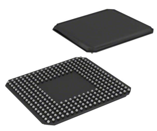
Architecture Overview:
The Intel EP4CE15F23I7N boasts a rich assortment of resources, including programmable logic elements, embedded memory blocks, high-speed transceivers, and dedicated input/output (I/O) pins. This flexible architecture enables designers to implement complex algorithms, signal processing chains, and control systems with precision and efficiency.
Key Features:
With features such as hardened processors, configurable DSP blocks, and advanced clocking resources, the EP4CE15F23I7N offers unparalleled flexibility and performance. These features are instrumental in meeting the demanding requirements of modern applications, including machine learning, image processing, and network acceleration.
Development Process:
To fully leverage the capabilities of the Intel EP4CE15F23I7N FPGA, developers must navigate through the stages of design, implementation, and validation with diligence and proficiency.
Design Entry:
Design entry can be accomplished using hardware description languages (HDL) such as Verilog or VHDL, or through graphical schematic entry tools. Intel's Quartus Prime Design Software provides a comprehensive platform for design entry, synthesis, and verification.
Synthesis and Optimization:
During synthesis, the HDL code is translated into a hardware netlist, which is then optimized for performance, area, and power consumption. Quartus Prime's synthesis and optimization tools enable designers to achieve the desired balance between these metrics while meeting stringent timing constraints.
Place and Route:
The place and route stage involves mapping the logical design onto physical FPGA resources and determining the routing of interconnections. Quartus Prime's advanced algorithms ensure optimal placement and routing, thereby maximizing performance and minimizing timing violations.
Testing and Validation:
Thorough testing and validation are imperative to ensure the reliability and functionality of the FPGA design.
Functional Simulation:
Functional simulation allows designers to verify the behavior of the FPGA design under different operating conditions and input stimuli. Comprehensive test benches and simulation tools facilitate rigorous testing and debugging.
Hardware Validation:
Once the design is synthesized, implemented, and verified through simulation, it is deployed onto a target FPGA device for hardware validation. Real-world testing validates the performance and functionality of the FPGA design in practical scenarios.
Conclusion:
The Intel EP4CE15F23I7N FPGA stands as a testament to innovation and engineering excellence, offering unmatched performance, versatility, and scalability. By mastering its architecture and development workflow, designers can unlock its full potential and realize groundbreaking solutions across diverse industries. Whether you're designing cutting-edge data processing systems, high-speed communication interfaces, or embedded control applications, the Intel EP4CE15F23I7N FPGA serves as a reliable and powerful enabler of technological advancement.
1 note
·
View note
Text
Agilex 5 E-Series with Power-Optimized Edge Performance
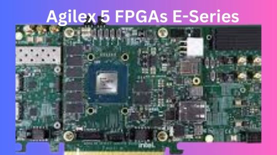
Intel Agilex 5 FGPA
Agilex 5 E-Series
Altera’s latest mid-range FPGAs, the Agilex 5 FPGAs E-Series, are now supported by the recently released Quartus Prime Software v24.1, which can be downloaded right now. Intel are happy to announce that it is now simpler than ever and completely free of charge to take use of the unmatched capability of Altera’s Agilex 5 FPGAs E-Series with the introduction of the state-of-the-art Quartus Prime Software from Altera.
Intel Agilex 5
Free Licence: Get rid of obstacles. With the help of Quartus Prime Pro Edition Software v24.1, you may use the newest E-Series devices at no cost, enabling you to innovate beyond limits!
Streamlined Design Flow: Use Quartus Prime Software to see the smooth integration of intellectual property (IP)-Centric design flow. Their easily customizable design samples streamline the process of getting started so you can concentrate on what really matters your innovative ideas.
New Embedded Processing Capabilities: Make use of the Simics simulator-supported dual-core ARM Cortex-A76 and dual-core ARM Cortex-A55 of the Agilex 5 SoC FPGA, the industry’s first asymmetric processing complex. Additionally, Agilex 5 FPGAs may be combined with the feature-rich, performance- and space-optimized Nios V soft-processor for smaller embedded FPGA applications. Additionally, they collaborate with a number of partners who provide a top-notch suite of tools to improve your FPGA and embedded development experience, including Arm, Wind River, Siemens, Ashling, MathWorks, and many more.
Comprehensive Intellectual Property (IP) Portfolio: With their tried-and-true IP portfolio for Agilex 5 FPGAs, many of which are free, you may shorten the time it takes to market. Reduce the amount of circuitry used and make design timing closure easier with hard IP solutions for PCI Express, Ethernet, and memory protocols, which also support LPDDR5. With PCS’s Ethernet 10G MAC, you can guarantee deterministic and synchronised communication, enhanced by Time-Sensitive Networking (TSN) features.
This version includes the Video and Vision Processing (VVP) portfolio IP for Agilex 5 FPGAs, which enables the entire portfolio of video solutions, as well as additional IPs supporting MIPI D-PHY and MIPI CSI-2. Begin developing your Agilex 5 FPGA designs and rely on additional validated advanced features like JESD204C IP, ORAN IP, LDPC IP, CPRI, and eCPRI among others.
Unprecedented Capabilities: Altera FPGAs may be programmed with cutting-edge capabilities like the following using the Quartus Prime Pro Edition Software v24.1.
Agilex 5 datasheet
Dashboard for Quartus Software Exploration (Preproduction)
With distinct instances of Quartus Prime software, numerous projects running concurrently may be easily coordinated and the compilation and timing results can be seen.
Fresh Features for Compilation: Generation flow of precompiled components (PCCs)Utilising the new precompiled component (PCC) generation flow during compilation, shorten the time it takes to compile synthesis.Start the Simulator using the Quartus Prime GUI.Effortlessly start simulations straight from the Quartus Prime GUI by using the handy “Tools ➤ Run Simulation” menu item. Remove the need for extra procedures to streamline your workflow and save time.
Features and Improvements of Synthesis
Use the RTL Linter Tool to convert older RTL files to Verilog/VHDL standards with ease, optimise RAM inference for better speed and resource use, and reduce warnings in error-free RTL modules to increase readability while developing.
Improved Timing Indicator
Gain more flexibility in timing analysis and SDC scripting with new scripting options; guarantee design integrity with sign-off capabilities for particular combinational loops; and learn more about timing characteristics with enhanced Chip Planner visualisation of asynchronous clock domain crossings (CDCs).
Innovations in Advanced Link Analysers
Link Builder: Use the brand-new Link Builder tool to quickly and easily build high-speed serial connections. Streamline the connection creation procedure by automatically generating schematics and importing channels and devices.
High DPI Monitor Assistance: Benefit from improved readability and display quality thanks to GUI scaling for high DPI displays and automated DPI recognition. Enjoy enhanced usability and user experience.
Enhanced Data Viewer: With improvements to the Data Viewer, analyse forward error correction (FEC) code word faults more effectively. Error outcomes may be easily interpreted and analysed for more efficient error correction techniques.
Enhancements to Simulation Time:
Easy-to-use UI for automated import of devices and channels and schematics. Agilex 7 IP offers faster simulation times with the updated Q run and FEC models.
Qualities:
R-Tile: Transaction Layer (TL) multi-channel DMA IP (AXI) up to Gen5 x16 For flexibility in incorporating third-party PCIe Switch IP, use the bypass mode. A new design example for Gen5 x4 endpoint configuration is also provided.
F-Tile: Utilising FastSIM to reduce simulation time in PIPE mode and providing Ubuntu driver support for all sample designs.increased compatibility for up to 64 embedded endpoints.For greater coverage, the Debug Tool Kit (DTK) was added to the switch IP.
Become a Part of the Community: Hua Xue, VP & GM Software Engineering, remarked, “Intel’re excited to offer Quartus Prime Software v24.1, a crucial milestone in FPGA design.”
“Now, engineers everywhere can easily access the unmatched potential of Agilex 5 FPGAs E-Series.” Quartus’s simplified design process and these cutting-edge technologies allow engineers to reach their full potential for innovation. With their state-of-the-art processing capabilities, Agilex 5 devices transform embedded FPGA applications. These are enhanced by Quartus’s vast IP portfolio, which includes a variety of solutions like Ethernet, PCI Express, memory protocols like LPDDR5, support for MIPI D-PHY, CSI-2, and a suite of video solutions, among many other IPs.
The Quartus Exploration Dashboard offers a user-friendly interface and optimization recommendations, which further improve the design exploration process. Intel’re pushing both the simplicity of use and the fast compiler technologies with Quartus v24.1’s open access to E-Series FPGAs and a simplified design pipeline to enable engineers and innovators to unleash their creativity like never before.”
Intel Agilex 5 price
Normally marketed to corporations and incorporated into bigger systems, the Intel Agilex 5 FPGAs do not have a set pricing that is made accessible to the general public. A number of variables affect the pricing, including:
Model specifics: The Agilex 5 family has two distinct series (D and E) with differing logic cell characteristics and capacities. Models with additional features will cost more.
Volume: If you buy in large quantities, you may be able to negotiate a lower price with distributors or directly with Intel.
Distributor: Price structures may vary significantly throughout distributors.
Read more on Govindhtech.com
#Agilex#intelagilex#agilex5#intelagilex5#govindhtech#FPGA#news#technews#technology#technologynews#TechnologyTrends Intel
0 notes
Text
VHDL Assignment #3: Design and Simulation of Adder Circuits
2 Learning Outcomes After completing this lab you should know how to: Use VHDL statements to implement different adder circuits Write efficient VHDL codes Perform functional simulation Perform basic timing analysis You will also have a better understanding of the concept of synthesis of logic circuits. 3 VHDL Description of Adder Circuits In this assignment, you will be asked to perform the…

View On WordPress
0 notes