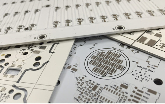
#Multilayer Metal Core PCB
Explore tagged Tumblr posts
Visit Tumblr Blog
Explore Tumblr blogs with no restrictions, modern design and the best experience.
Last Seen Tumblr Blogs


Fun Fact
The Tumblr office adopted Tommy, an 11-year-old Pomeranian.
Text
PCB Manufacturers in India: Powering the Future of Electronics
India is steadily emerging as a key global player in the electronics industry, with Printed Circuit Board (PCB) manufacturing at its core. PCBs form the essential backbone of every electronic device, from smartphones and laptops to advanced defense systems and electric vehicles.
As the electronics sector in India continues to thrive, PCB manufacturers in India are expanding their capabilities, delivering high-quality, cost-effective solutions to meet both domestic and global demands. This article explores India’s PCB manufacturing ecosystem and highlights some of the leading companies driving this growth.
Why PCB Manufacturers in India Are in High Demand
The growth of PCB manufacturing company in India is driven by several significant factors:
Government Initiatives
Government programs such as Make in India and the Production Linked Incentive (PLI) Scheme have provided a major boost to the electronics manufacturing sector, encouraging domestic PCB production and reducing dependency on imports.
Rising Electronics Consumption
The increasing use of electronics in industries such as automotive, telecom, defense, consumer appliances, and renewable energy has created a surging demand for quality PCB fabrication.
Competitive Advantage
Indian PCB manufacturers combine cost-effectiveness, skilled engineering, and adherence to international quality standards, making them competitive not just in India but also in international markets.
Export Capabilities
Many Indian PCB companies now actively export to global markets, particularly in Europe, the United States, and Southeast Asia, expanding India’s presence in the international supply chain.
Leading PCB Manufacturers in India
Below is a curated list of some of the top PCB manufacturers in India, known for their expertise, innovation, and commitment to quality:
AT&S India Pvt. Ltd.
Location: Nanjangud, Karnataka AT&S India, a subsidiary of Austria-based AT&S Group, specializes in advanced high-density interconnect (HDI) and multilayer PCBs, catering to automotive, industrial, and medical device industries.
Shogini Technoarts Pvt. Ltd.
Location: Pune, Maharashtra With over four decades of experience, Shogini Technoarts focuses on single-sided and double-sided PCBs, supplying sectors like automotive, telecom, and lighting.
Genus Electrotech Ltd.
Location: Gandhidham, Gujarat Genus Electrotech is a leading fully integrated electronics manufacturer producing PCBs alongside complete electronics assemblies, widely used in energy meters, LED lighting, and automotive electronics.
Circuit Systems India Ltd. (CSIL)
Location: Gandhinagar, Gujarat CSIL manufactures multilayer PCBs for industries such as telecommunications, aerospace, automotive, and consumer electronics, known for precision and high reliability.
Anand Electronics
Location: Bengaluru, Karnataka Anand Electronics produces single, double, and multilayer PCBs, catering to customers in automation, LED lighting, power electronics, and industrial systems.
Meena Circuits Pvt. Ltd.
Location: Gandhinagar, Gujarat Meena Circuits specializes in multilayer PCBs and metal core PCBs (MCPCBs), supporting power electronics, automotive components, and LED applications.
Hi-Q Electronics Pvt. Ltd.
Location: Mumbai, Maharashtra Hi-Q Electronics offers customized PCB solutions, including flexible and rigid-flex PCBs, for sectors such as aerospace, defense, medical devices, and industrial machinery.
Epitome Components Ltd.
Location: Aurangabad, Maharashtra One of India’s largest producers of single-sided PCBs, Epitome Components supplies to major OEMs in the consumer electronics and lighting sectors both domestically and internationally.
Fine-Line Circuits Ltd.
Location: Mumbai, Maharashtra Fine-Line specializes in prototype and production PCBs, especially multilayer rigid PCBs, for demanding applications in defense, aerospace, and telecommunications.
SFO Technologies (NeST Group)
Location: Kochi, Kerala Part of the global NeST Group, SFO Technologies provides advanced PCB fabrication services, serving high-end industries such as aerospace, defense, medical, and industrial electronics worldwide.
Benefits of Choosing PCB Manufacturers in India
Selecting PCB manufacturers in India offers businesses several clear advantages:
International Certifications: Most Indian manufacturers are certified with ISO, UL, IPC, and RoHS standards.
Wide Range of Capabilities: From single-sided to multilayer, flexible, and HDI PCBs.
Engineering Support: Many manufacturers provide design support, prototyping, and customization.
Global Reach: Indian manufacturers export to several developed markets, showcasing reliability and trustworthiness.
The Road Ahead for PCB Manufacturing in India
As India continues to strengthen its electronics manufacturing ecosystem, the PCB industry will play a vital role in achieving self-reliance and reducing imports of critical components. With investments in automation, advanced machinery, and sustainable manufacturing practices, Indian PCB manufacturers are well-positioned to meet global demand.
Conclusion: Partner with the Best PCB Manufacturers in India
Whether you are designing innovative IoT solutions, building critical EV systems, or developing specialized equipment for aerospace or defense, India’s PCB manufacturers can provide world-class solutions tailored to your needs.
If you’re searching for reliable and experienced PCB manufacturing partners, explore the top suppliers on FindingMFG. Connect with trusted PCB fabrication companies and accelerate your product development journey.
Visit FindingMFG.com today to discover the leading PCB manufacturers in India for your next project
0 notes
Text
Learn the Traits to Find the Best Mcpcb Manufacturer for Your Needs
Metal-core printed circuit boards are one of the most significant spare parts you need to operate and control electronic goods. The quality of this spare will affect the functioning of the entire device. Hence, the manufacturers and the suppliers of the product are some of the elemental stakeholders for electronic device-producing brands. Naturally, due to massive demand, you can find several makers and suppliers in the industry. In this article, we will discuss the traits to discern the best.
Years of experience
The first aspect which you must find out to work with the best mcpcb manufacturer is the number of years for which the company has been operational in the market. You must look for a brand which has been in the market for a minimum of one and a half decades.
Service Array
Services from the top manufacturers and suppliers can help patrons get the best value for their investment. Some of the vital services you can get from the market leaders is mcpcb assembly, mass production, product prototype and innovative designing. These brands are masters in customization and they can change and adapt their products as per the precise customer requirements.
Product Array
Apart from service variety these brands can also act as some of the best single window service providers for different products like single layer metal core pcb, double sided metal core pcb, two layer aluminum base pcb and multilayer aluminum base pcb. Hence irrespective of your requirement specifications you can turn to a single vendor to meet all your business needs.
Quality control certificate
Finally, before you select a vendor for your business one of the main things which you must check is quality assurance certifications for the products from the vendor. This is one of the parameters that give you assurance for the product quality into which you are investing and also for their internal procedures and organization culture. These are the vendors who can add much value to your business.
0 notes
Text
Viasion Technology: Your Trusted Partner for Quality PCB Manufacturing Solutions
In today’s fast-paced tech world, electronics are everywhere—from smartphones and wearables to medical devices and industrial systems. Behind every smart gadget or complex system lies a network of well-designed printed circuit boards (PCBs) that bring it all to life. At Viasion Technology, we’re proud to be one of the most trusted names in PCB manufacturing, offering high-quality, customized PCB solutions to companies all over the world.
Whether you're a startup prototyping a new device or an established business scaling up production, Viasion is here to help you turn your ideas into reality—with precision, reliability, and cost-efficiency at the core of everything we do.
Why Choose Viasion for Your PCB Needs?
Since 2007, Viasion has been delivering exceptional PCB fabrication and assembly services from our headquarters in Shenzhen, China. With over 17 years of experience, we’ve served clients across various industries, including medical, automotive, industrial control, IoT, and consumer electronics.
Our team combines engineering expertise with state-of-the-art technology to ensure every board we produce meets the highest international standards. From prototype to production, we offer end-to-end services that help streamline your product development cycle.
Comprehensive PCB Capabilities
At Viasion, we understand that no two projects are the same. That’s why we offer a broad range of PCB types and services to meet your exact technical and budgetary requirements. Some of our core offerings include:
1. Copper PCB Board Manufacturing
Copper PCB boards are the backbone of modern electronics. They offer superior conductivity, excellent heat dissipation, and high durability—perfect for high-power applications. Whether you need single-layer, double-layer, or multi-layer copper boards, we have the expertise to deliver consistent quality.
Our copper PCBs are widely used in LED lighting, power electronics, automotive systems, and more. Plus, we offer a range of thickness options and custom finishes to suit your specific needs.
2. Flex PCB and Flex PCB Board Production
Looking for a lightweight, space-saving alternative to traditional rigid PCBs? Flex PCBs (also known as flex PCB boards) are your go-to solution. These boards can bend, twist, and fold, making them ideal for compact devices and dynamic applications.
At Viasion, we manufacture high-quality flexible boards that perform well under stress and resist vibration. Whether you need single-sided, double-sided, or multilayer flexible circuit boards, our team can guide you through the entire process—from material selection to final inspection.
3. Flexible Circuit Board Solutions
Our flexible circuit board options are engineered for durability and versatility. These boards are especially useful in wearable tech, mobile phones, and aerospace systems where space and weight are critical concerns.
We ensure that each flexible PCB goes through rigorous testing to meet the most demanding requirements. With Viasion, you can count on flexible solutions that don’t compromise on performance.
4. FR4 PCB Manufacturing
FR4 is one of the most popular materials used in PCB production due to its excellent strength-to-weight ratio and thermal resistance. Our FR4 PCB solutions are suitable for everything from simple consumer electronics to high-end industrial controls.
We offer FR4 boards in various thicknesses, copper weights, and surface finishes. Whether you’re building a prototype or scaling to mass production, we’ll make sure your FR4 PCBs are manufactured to your exact specs.
5. Metal Core PCB (MCPCB) Fabrication
If your project demands superior thermal management, our metal core PCB (MCPCB) options are the ideal choice. With aluminum or copper cores, these boards can efficiently dissipate heat, which is crucial in high-power LED and automotive applications.
At Viasion, we manufacture single-sided, double-sided, and multilayer MCPCBs that combine thermal performance with electrical reliability. Our advanced manufacturing techniques ensure minimal thermal resistance and excellent mechanical strength.
Industries We Serve
Our PCBs are found in a wide array of products across industries, including:
Automotive: Durable and heat-resistant PCBs for electric vehicles and ADAS systems.
Medical Devices: High-precision boards for diagnostic equipment and patient monitoring systems.
Industrial Control: Reliable PCBs for automation, robotics, and smart manufacturing.
Consumer Electronics: Compact and cost-effective boards for wearables, smart gadgets, and more.
IoT Applications: Custom PCB solutions optimized for wireless communication and low-power consumption.
What Sets Viasion Apart?
✅ Experienced Team – Our engineers have years of hands-on experience in PCB design, manufacturing, and testing.
✅ Advanced Facilities – Our ISO9001, ISO13485, and UL-certified factory is equipped with modern machines and inspection tools.
✅ Flexible Order Quantities – From one-off prototypes to full-scale production, we can handle orders of any size.
✅ Strict Quality Control – Every board goes through electrical testing, AOI inspection, and functional checks before shipping.
✅ Global Reach, Local Support – While we’re based in China, we serve clients worldwide, offering responsive communication and fast lead times.
Getting Started with Viasion
Starting a project with us is easy. Just send your PCB Gerber files and specifications, and we’ll get back to you with a quick quote. Need help optimizing your design for manufacturing? Our team offers DFM (Design for Manufacturability) feedback at no additional cost.
We’re more than just a manufacturer—we’re your engineering partner every step of the way.
Let’s Build Something Great Together
Whether you’re working on a next-gen wearable or an industrial control system, you need a PCB partner you can trust. At Viasion Technology, we combine technical know-how with personalized service to deliver PCBs that meet your performance and budget expectations.
From copper PCB boards and flexible circuit boards to FR4 PCBs and metal core PCBs, we’ve got you covered with comprehensive capabilities and a proven track record.
0 notes
Text
Top-Tier PCB Fabrication Services for Every Industry
High-performance printed circuit boards (PCBs) continue growing across every industry. From consumer electronics to aerospace, medical devices to automotive systems, the quality of a PCB can determine the performance, efficiency, and durability of an entire product. That's why top-tier PCB fabrication services are more critical than ever — and why choosing the right PCB fabrication company can make or break your success.
At the heart of every advanced electronic product lies a well-engineered PCB. As a trusted PCB manufacturing company, our mission is to deliver high-quality, precision-fabricated PCBs that meet the specific needs of your project, no matter how simple or complex.
Precision Engineering for Maximum Performance
Our PCB fabrication services are built on a foundation of engineering excellence. We use state-of-the-art technology and a highly skilled team to produce PCBs that meet tight tolerances and rigorous quality standards. Whether you're working with a standard double-sided design or a multilayer, high-density interconnect (HDI) board, we have the capability to deliver with precision.
Key fabrication capabilities include:
Single, Double, and Multilayer PCBs
HDI and Rigid-Flex Boards
High-Frequency & High-Speed PCBs
Heavy Copper & Metal Core PCBs
Lead-Free & RoHS Compliant Options
Through Hole PCB Assembly and Surface Mount Technology (SMT)
Each board is fabricated using high-grade materials and strict process control to ensure superior reliability and performance in real-world applications. Whether you need quick turn PCB assembly services for a prototype or a full-scale production run, we’re ready to meet your deadline.
Serving a Broad Spectrum of Industries
What sets us apart as a full-service PCB manufacturing company is our versatility. We support customers across a wide range of industries, offering specialized expertise in each vertical:
Consumer Electronics – Smartphones, wearables, and smart appliances require compact, high-speed PCBs with impeccable performance.
Automotive – From powertrain systems to in-car infotainment, automotive electronics rely on durable, high-temperature-resistant boards.
Medical Devices – Life-saving equipment like imaging systems and portable monitors demand extreme precision and zero-defect standards.
Industrial Automation – PCBs for control systems, robotics, and sensors must withstand harsh environments and continuous operation.
Telecommunications – Our fabrication processes support high-frequency RF boards essential to telecom infrastructure and 5G devices.
Aerospace & Defense – We offer military-grade fabrication for mission-critical electronics with strict adherence to industry standards.
No matter your application, our team works closely with you to understand your technical requirements and deliver boards that exceed expectations.
Customized PCB Fabrication Solutions
Every project is unique, and we believe in delivering tailored solutions that align with your product's performance, budget, and production timeline. As an experienced PCB fabrication company, we provide comprehensive design-to-delivery support to streamline your workflow.
Whether you're at the prototyping stage or preparing for full-scale production, we offer:
Quick-Turn Prototyping
Small to High-Volume Production
Custom Stackups & Impedance Control
Material Selection Guidance
DFM (Design for Manufacturability) Feedback
Quick Turn PCB Assembly Services to accelerate product development
Our design support team is available to review your Gerber files, assist with layout optimization, and ensure that your design is perfectly matched to our manufacturing capabilities.
Uncompromised Quality and Certification Standards
Quality is non-negotiable. All our fabrication processes are governed by international standards and robust quality management systems. We conduct multi-stage inspections and automated optical testing (AOI) at every critical phase of production.
Certifications and quality assurances include:
ISO 9001:2015 Certified
IPC Class 2 & Class 3 Compliant
UL Certification
RoHS and REACH Compliance
Full Traceability of Materials and Processes
Whether it's high-volume orders or through hole PCB assembly projects with complex layouts, our goal is to deliver zero-defect PCBs that perform flawlessly in their intended environment, every single time.
Fast Turnaround and On-Time Delivery
In fast-moving markets, time-to-market is everything. That’s why we offer quick turn PCB assembly services with guaranteed lead times, giving you the flexibility to meet tight project deadlines without compromising on quality.
Our streamlined workflow, in-house capabilities, and experienced logistics team ensure that your PCBs are delivered on time and ready for assembly — whether you're local or overseas.
Your Trusted PCB Fabrication Partner
Partnering with us means more than just placing an order — it means gaining a dedicated team invested in your product’s success. As a full-service PCB fabrication company, our focus on innovation, precision, and customer service has made us a trusted name in the electronics manufacturing industry for startups, engineers, and Fortune 500 companies alike.
We invite you to experience the difference of working with a fabrication house that puts your needs first.
Let’s Build the Future Together
Ready to get started? Whether you have a complex multilayer board, a custom design requiring through hole PCB assembly, or need quick turn PCB assembly services, our expert team is here to help you move from concept to reality — faster and better than ever before.
Contact us today for a free quote or design consultation, and discover how a trusted PCB manufacturing company can elevate your next project.
Let me know if you'd like this adapted into a landing page, brochure copy, or SEO-optimized blog!
0 notes
Text
Metal core PCBs, or MCPCBs, including single layer metal core PCB, double layer metal core PCB and multilayer metal core PCB, are widely used in high-power LED lighting applications, automotive electronics, and other fields. HITECHPCB is a trusted metal core PCB manufacturer in China. We offer metal core PCB prototyping, single-layer copper core PCB, double-side MCPCB, and multilayer MCPCB manufacturing services.
0 notes
Text

What is the difference between ceramic, high frequency and ordinary PCB boards?
Ceramic substrate is a kind of special PCB board with good thermal conductivity, insulation performance, and high dielectric constant. It is widely used in terminal products in the field of heat dissipation. Commonly used ceramic-based materials include aluminum oxide, aluminum nitride, zirconium oxide, ZTA, silicon nitride, silicon carbide, etc. FR circuit board refers to a circuit with epoxy glass fiber cloth as the main material. So, what is the difference between ceramic circuit board and ordinary PCB board
The difference between ceramic substrate and PCB board
Different materials. Ceramic substrate is an inorganic material, and the core is aluminum oxide or aluminum nitride; ordinary PCB board uses FR4 glass fiber board, which is an organic material. Ordinary PCB board can be laminated in multiple layers. LTCC is the mainstream of ceramic multilayer circuit board. The ceramic multilayer process currently being developed by Hitech Circuits Co., Ltd. is different from the traditional method. It uses magnetron sputtering technology to grow a layer of ceramic medium on the ceramic circuit board that has been metallized, and then re-metallizes this layer of medium to make the second layer of circuit.
b. The performance and application of ceramic substrates are different. The thermal conductivity of ceramic substrates far exceeds that of ordinary PCB boards. The thermal conductivity of alumina ceramics is ≧25W(m·K), and the thermal conductivity of aluminum nitride ceramics is ≧170W(m·K). They are used in industries with large heat dissipation requirements, such as high-power LED lighting, high-power modules, high-frequency communications, and track power supplies. The thermal expansion coefficient of ceramic substrates is more compatible with silicon wafers, and the product stability is higher. Ordinary PCB boards are widely used, mostly in private commercial products.
The difference between ceramic substrates and high-frequency boards
Different materials. Ceramic substrates are made of aluminum oxide or aluminum nitride, while high-frequency boards are mostly made of Rogers, Yalong, polytetrafluoroethylene, etc., with low dielectric constants and fast high-frequency communication speeds.
Different performance. Ceramic substrates are widely used in cooling sheets and systems, high-power modules, automotive electronics and other fields. High-frequency PCB boards are mainly used in high-frequency communications, aviation, high-end consumer electronics, etc.
3. In the field of high-frequency communications involving heat dissipation requirements, ceramic substrates are usually required to be combined with high-frequency PCB boards, such as high-frequency ceramic PCBs.
If you want to know ceramic PCBs, please feel freely to contact Cynthia at [email protected]
0 notes
Text
Elevating Electronics: Multilayer PCBs with High Copper Thickness and Aluminum Base by sqpcb.com

In the ever-evolving landscape of electronic components, Multilayer PCBs have emerged as the linchpin, enabling the development of complex and high-performance devices. Among the myriad options available, Multilayer PCBs with high copper thickness and Aluminum base PCBs have garnered attention for their exceptional capabilities. At the forefront of this technological innovation stands sqpcb.com, a leading provider of high-quality PCB manufacturing solutions.
Exploring Multilayer PCBs with High Copper Thickness
Multilayer PCBs with high copper thickness are engineered to accommodate increased current carrying capacity, better thermal management, and enhanced durability. These boards feature thicker copper layers, ensuring robustness and improved performance in demanding applications.
Advantages of High Copper Thickness Multilayer PCBs:
Enhanced Power Capability: The thicker copper layers enable higher current-carrying capacity, crucial for power electronics, high-power LEDs, and motor control systems.
Improved Thermal Management: Enhanced copper thickness aids in better heat dissipation, reducing the risk of overheating and ensuring the longevity of electronic components.
Greater Durability: High copper thickness contributes to the board's mechanical strength, making it more resistant to wear and tear, ideal for applications subjected to harsh conditions.
Unveiling Aluminum Base PCBs
Aluminum base PCBs, also known as Metal Core PCBs (MCPCBs), offer a unique advantage with their aluminum substrate, providing excellent thermal conductivity and heat dissipation capabilities.
Key Features of Aluminum Base PCBs:
Efficient Heat Dissipation: The aluminum base acts as a superior heat sink, drawing heat away from sensitive components, making them ideal for high-power LED lighting, automotive applications, and power converters.
Lightweight and Durable: Aluminum's lightweight nature coupled with its durability makes these PCBs suitable for applications where weight is a concern, without compromising on performance.
Leading the Innovation: sqpcb.com
Sqpcb.com distinguishes itself by offering an array of Multilayer PCBs with high copper thickness and Aluminum base PCBs, catering to diverse industry needs.
Specialized Expertise: Their specialization in manufacturing PCBs with high copper thickness ensures precise etching and lamination processes, maintaining the integrity of thicker copper layers.
Aluminum Base PCB Excellence: Sqpcb.com's prowess in Aluminum base PCB fabrication lies in their understanding of thermal management, ensuring optimal design for heat dissipation.
Quality Assurance: With stringent quality control measures in place, sqpcb.com ensures that every board manufactured meets industry standards and client specifications.
Conclusion
Multilayer PCBs with high copper thickness and Aluminum base PCBs represent technological milestones in the electronics industry, addressing the demands for increased power capability, thermal management, and durability. Sqpcb.com's commitment to innovation and precision manufacturing further elevates these PCB variants, catering to the evolving needs of diverse industries.
For businesses and engineers seeking superior performance and reliability in their electronic designs, sqpcb.com emerges as a trusted partner, delivering excellence in Multilayer PCBs with high copper thickness and Aluminum base PCBs.
#Multilayer PCB#Aluminium PCB Board#Customize PCB#Customized PCB Boards#PCB Board#Printed Circuit Board
0 notes
Text
Multilayer pcb is circuit boards composed of two or more conductive layers (copper layers). The copper layer is pressed together by the resin layer (prepreg).
King Credie manufacture multilayer pcb up to 32 Layer ,We accept pure single material or mixed-press materials ( e.g., FR4,Rogers,Polymide,metal Core).
#Multilayer PCB Stackup Design#Multilayer PCB Design#Multilayer Stackup Design#Multilayer Stackup#PCB Stackup Design#Stackup Design#PCB Design#Multilayer Design#Multilayer PCB Stackup#Multilayer construct Design
0 notes
Link

#PCB#PCBs#PCBA#Printed Circuit Board#Printed Circuit Board Assembly#PCB Prototype#PCB Manufacturer#Metal Core PCB#Metal Core Printed Circuit Board#Technotronix#Manufacture Metal core PCB#PCB Company#PCB Industry#PCB Assembly Services#PCB Fabrication#Metal PCBs#Multilayer Metal Core PCB#Metal Core Bare Boards#USA#California
0 notes
Text
Durable Metal Clad PCBs for High-Efficiency Thermal and Electrical Performance
In industries where thermal management, durability, and high electrical performance are non-negotiable, metal clad PCBs have become a top choice. ASC International offers top-tier metal clad PCB solutions designed to deliver exceptional thermal conductivity, mechanical strength, and electrical reliability. Whether you're designing for automotive, industrial, or high-power applications, our metal clad PCBs ensure your products can handle the most demanding environments.
What is a Metal Clad PCB?
A metal clad PCB integrates a metal base, typically aluminum or copper, into the standard PCB design. This metal base serves as an efficient heat sink, transferring heat away from the components to prevent overheating and damage. Unlike conventional PCBs that use fiberglass or composite materials, metal clad PCBs use a dielectric layer between the metal base and the copper layer to ensure electrical isolation while still allowing for optimal thermal dissipation.
The result is a robust circuit board that offers not only excellent heat management but also superior mechanical strength and electrical performance.
Why Metal Clad PCBs Are Essential
The primary reason metal clad PCBs are chosen for specific applications is their ability to manage heat efficiently. Here’s why metal clad PCBs are essential:
Efficient Thermal Dissipation: Metal core PCBs effectively transfer heat from high-power components, preventing overheating and extending the lifespan of electronics.
Mechanical Strength: The metal base adds an extra layer of mechanical durability, which helps prevent warping or bending that can occur in traditional PCBs.
Compact Design Flexibility: With superior heat management, designers can place components closer together, allowing for more compact and efficient circuit board designs.
Reliable Electrical Performance: Metal clad PCBs provide stable electrical performance with minimal signal interference, making them ideal for high-frequency or power-intensive applications.
Increased Product Lifespan: With better thermal management, the overall stress on components is reduced, leading to a longer and more reliable operational life for electronic devices.
Our Metal Clad PCB Solutions
At ASC International, we provide a diverse selection of metal clad PCB solutions to suit a variety of industries and applications:
Aluminum-Based Metal Clad PCBs: Known for their excellent thermal conductivity and lightweight properties, aluminum-based metal clad PCBs are the go-to choice for applications like LED lighting, automotive systems, and power supplies.
Copper-Based Metal Clad PCBs: For applications requiring higher thermal and electrical performance, copper-based PCBs are the ideal solution, offering superior conductivity and heat dissipation.
Multilayer Metal Clad PCBs: For complex designs with multiple layers, we offer multilayer metal clad PCBs that provide high-density circuit layouts while maintaining excellent thermal and mechanical properties.
Custom Metal Thickness Options: Tailor your metal clad PCB with different metal thicknesses to optimize the heat dissipation, mechanical strength, and flexibility required for your specific application.
Applications of Metal Clad PCBs
Due to their superior thermal and mechanical properties, metal clad PCBs are widely used in industries where heat management and durability are essential:
LED Lighting: Metal clad PCBs are crucial for LED applications, as they effectively manage the heat generated by high-power LEDs, ensuring optimal brightness and longevity.
Automotive Electronics: From engine control modules to safety systems, metal clad PCBs can withstand extreme temperatures and mechanical stress in automotive applications.
Power Electronics: Power supplies, inverters, and motor controllers rely on metal clad PCBs to handle high currents and dissipate the heat generated by power components.
Telecommunications Equipment: In communication infrastructure, metal clad PCBs maintain signal integrity and reduce heat buildup, ensuring stable and reliable operation.
Industrial Control Systems: Metal clad PCBs ensure that industrial equipment, automation systems, and control panels operate reliably under demanding conditions.
Why Choose ASC International for Metal Clad PCBs?
When it comes to high-quality metal clad PCB manufacturing, ASC International is a trusted partner. Here’s why:
Industry Expertise: With years of experience in PCB manufacturing, we specialize in delivering solutions tailored to your specific needs, ensuring that your designs are both efficient and reliable.
Precision Manufacturing: We use state-of-the-art equipment and processes to guarantee consistent quality, whether you require small runs for prototyping or large-scale production.
Custom Solutions: We work closely with our clients to provide custom metal clad PCB designs that meet exact specifications, including unique material, thickness, and layer configurations.
Quality Assurance: Our products undergo strict quality control tests, ensuring each metal clad PCB meets high standards for electrical performance, mechanical strength, and thermal management.
On-Time Delivery: We understand the importance of timelines and provide reliable delivery schedules to keep your project on track.
Get in Touch with ASC International
ASC International is here to help you with your metal clad PCB requirements. Whether you need a single-layer or multilayer PCB, aluminum or copper base, we offer tailored solutions to ensure your designs perform optimally in the real world.
Contact us today to learn more about our metal clad PCB offerings, get a quote, or discuss how our solutions can help improve the performance, durability, and efficiency of your products.
0 notes
Photo

Studio Silkraft is PCB manufacturer and EMS service providers based in Bahadurgarh, Haryana (Delhi-NCR). We manufacture Single Sided PCB (FR-1, CEM-1, FR-4), Double Sided PCB (PTH/Non-PTH), Multilayer PCB (Up to 28 layers) and Metal Core PCB. Established in the year 1966, we have an experience of Over 53+ years of experience in PCB manufacturing.
2 notes
·
View notes
Text
Understanding Characteristics Of A Standard Printed Circuit Board
Electronic gadgets run with a printed circuit board (PCB), a piece of an electronic chip that helps users to monitor them. All kinds of electrical goods you use daily rely on the circuit board implanted in the core system.
It provides a path for electrical current to flow in different directions. However, most people do not know the features and functions of circuits despite being familiar with electrical tools with PCBs.
From kitchen appliances to computers, these daily-use products contain printed circuits. Here are points to note down about PCBs used in assembling electrical items.
Understanding PCB
There was a time when a product running with electrical energy occupied extra space so that it could fit in wires and switches. Today, smart technology enables electronic manufacturers to constitute all the components into one metal-core printed circuit board.
Minimizing the circuit system ensures efficiency and economics because it lessens the size and number of items. Whenever you turn on an electronic device, the circuit board allows components in different areas around the board to transmit the signal to one another.
Features of a PCB
Some circuits are large and easy to detect in the product, while others come with tiny complex arrangements inside. A standard PCB may have a metal plate on which copper tracks and green-red run into specific routes under the protective cover.
The process of removing the cover of an integrated circuit requires IC chemical decapsulation. This tactic helps reveals the microparticles imprinted on the circuit when assessing the product data.
General components of PCB
A circuit board includes a wide range of mini components connected to different parts in a formidable pattern. Some widely known components of the PCBs are:
Battery: It provides energy to the circuit through its multiple terminals.
Capacitor: It has two terminals to store electrical energy in an electric field
Resistor: This electronic component regulates the flow of electric current.
Inductor: It is a conducting coil introducing inductance into a circuit.
Transistors: It is a semiconductor devices capable of amplification.
Diode: It is a semiconductor device consisting of a p-n junction.
PCB types
Electronic goods may comprise circuit board types based on their applications and functions. They can be of different shapes, sizes, and designs suitable for the product. The most common PCB types include:
Single-sided PCBs with only one layer of copper foil and an alloy case protecting the board.
Multilayer PCBs are versatile for rigid and flexible parts of the product. They usually have supporting layers on the configuration's sides, top, and bottom.
Rigid-Flex PCBs keep the board from moving and twisting when inserting multiple wire fittings into the circuit.
Companies developing electronic goods must choose the circuit board specially designed for the product. Find leading manufacturers of PCBs that offer integrated circuits with automated decapsulation to meet recommended criteria.
Author’s Bio: The writer is an avid online blogger. This article is about ic chemical decapsulation.
0 notes
Text
Defouling and pitting technology of rigid flexible printed circuit board
To drill the dirt and pitting is just after the flexible printed circuit board nc drilling, chemical plating of copper or copper plating directly in front of an important working procedure, just flexible printed circuit board to achieve reliable electrical interconnection, just flexible printed circuit board must be combined with its special materials, polyimide materials for its main body and the characteristics of acrylic acid is not resistant to strong alkali, choose suitable to drill and pitting.There are two kinds of technology of defouling and pitting technology of rigid flexible printed circuit board: wet method and dry method.
The wet drilling and defouling and pitting technology of rigid flexible printed circuit board consists of the following three steps:
1. Swelling (also called swelling treatment).The surface area that can be oxidized can be increased by softening the pore wall substrate with alcohol ether bentonite, which can be easily oxidized. Generally, butylcarbiol is used to make the pore wall substrate dissolve and expand.

2. Oxidation.The purpose is to clean the hole wall and adjust the charge of the hole wall.
(1) concentrated sulfuric acid method: because concentrated sulfuric acid has strong oxidation and water absorption, most of the resin can be carbonized and form water-soluble alkyl sulfonates to be removed. The reaction formula is as follows: CmH2nOn+H2SO4--mC+nH2O perforated wall resin drilling pollution effect is related to concentration of concentrated sulfuric acid, treatment time and solution temperature.The concentration of concentrated sulfuric acid used for the removal of drilling dirt shall not be less than 86% and 20-40 seconds at room temperature.Concentrated sulfuric acid only works on resin, but is not effective for glass fiber. After concentrated sulfuric acid is used to concave the hole wall, there will be glass fiber head protruding, which needs to be treated with fluoride (such as ammonium fluoride or hydrofluoric acid).When using fluoride to treat prominent glass fiber heads, technological conditions should also be controlled to prevent core absorption due to excessive corrosion of glass fiber. The general process is as follows:
- H2SO4:10%
NH4HF2:5-10 g/l
Temperature 30 ℃ in time: 3 to 5 minutes
According to this method of punch after just - flexible printed circuit board to drill the dirt and pitting, and then the hole metallization, through metallographic analysis, found the inner drilling sewage didn't go to complete, lead to low copper layer and hole wall adhesion, thermal stress experiment in metallographic analysis for this (288 ℃, 10 + 1 second), the hole wall copper layer falls off and cause the inner circuit.
In addition, ammonium hydrogen fluoride or hydrofluoric acid have great toxicity, wastewater treatment is very difficult.What's more, polyimide is inert in concentrated sulfuric acid, so this method is not suitable for drilling, cleaning and pitting of rigid-flexible printed circuit board.
(2) the chromate method: because of chromic acid has strong oxidizing, its erosion ability is strong, so it can make the hole wall polymer material long chain disconnected, and oxidation and sulfurization, generated in the surface more hydrophilic groups, such as carbonyl (- C = O), hydroxyl (OH), sulfonic group (- SO3H), etc., so as to improve its hydrophilicity, adjust the hole wall charges, and to remove the purpose of the wall of hole drilling sewage and pitting.The general process formula is as follows:
Chromic anhydride CrO3:400 g/l
H2SO4:350 g/l sulphate
Temperature: 50 to 60 ℃ time: 10-15 min
According to this method, the rigid-flexible printed circuit board after drilling is defouled and corroded, and then the hole is metallized. The metallized hole is analyzed in metallography and tested in thermal stress.
Therefore, chromic acid method is also suitable for drilling, cleaning and pitting of rigid-flexible printed circuit boards. For small enterprises, this method is very suitable, simple and easy to operate.
(3) basic potassium permanganate method:At present, a lot of PCB manufacturers because of a lack of professional technology, still follow rigid multilayer printed circuit board is to drill the dirt and pitting technology - alkaline potassium permanganate to handle just - flexible printed circuit board, the method to remove resin after drilling sewage, at the same time can make its surface etching resin surface produce small bumpy small holes, in order to improve the adhesion strength of coating and the substrate of hole wall, under high temperature and high alkali environment, swelling of the resin can be removed using potassium permanganate oxidation drilling sewage, the system is work for the general rigid laminated, but for just - flexible printed circuit board does not adapt,Because polyimide, the main insulating base material of the rigid-flexible printed circuit board, is not resistant to alkaline, it needs to swell or even dissolve a little in alkaline solution, especially in high temperature and alkaline environment.If this method is adopted, even if the rigid-flexible printed circuit board is not scrapped at that time, the reliability of the equipment using the rigid-flexible printed circuit board will be greatly reduced in the future.
3. Neutralization.After oxidation treatment, the substrate must be cleaned and clean to prevent contamination of the activated solution in the later process. For this reason, it must go through the process of neutralization and reduction.
At present, the popular dry method at home and abroad is plasma decontamination and pitting technology.Plasma is used in the production of rigid-flexible printed circuit board, which is mainly used for drilling and cleaning the hole wall and surface modification of the hole wall.The reaction can be looked at is a highly active state of plasma with the hole wall polymer materials and glass fiber of gas and solid phase chemical reaction, the generated gas products and reaction of particles are not drain the process of vacuum pump, is a dynamic process of chemical reaction equilibrium. According to the first polymer materials used in the flexible printed circuit board usually choose N2, O2, the CF4, gas was fed as raw gas. The N2 have the effect of clean vacuum and preheating.
The schematic expression of plasma chemical reaction of O2+CF4 mixed gas is:
O2 + CF4O + OF + CO + COF package + + e - + F....
[plasma]
Due to the acceleration of electric field, it becomes a highly active particle and collides with O and F particles, resulting in high activity free radicals of oxygen and fluorine, etc., which react with polymer materials as follows:
[C, H, O, N] + [O+OF+CF3+CO+F+...]The CO2 + HF + H2O + NO2 +...
The reaction of plasma and glass fiber is:
SiO2 + [O + OF + CF3 + CO + + F...SiF4 + CO2 + CaL
At this point, we have realized the plasma treatment of the printed circuit board.
It is worth noting that the carbonylation reaction between O in atomic state and c-h and C=C leads to the addition of polar groups on the polymer bonds and the improvement of the surface hydrophilicity of polymer materials.
The rigid - flexible printed circuit board treated by O2+CF4 plasma and then treated with O2 plasma can not only improve the wettability (hydrophilicity) of the pore wall, but also remove the reaction.The finished sediments and incomplete intermediates.After the treatment of the rigid-flexible printed circuit board with direct electroplating, the metallized hole was analyzed in metallographic analysis and thermal stress test using plasma technology to drill dirt and cavitation, and the results fully met the gjb962a-32 standard.
In conclusion, both dry method and wet method can achieve the purpose of defouling and concave etching of the rigid-flexible interconnect motherboard if the proper method is chosen according to the characteristics of the main material of the system.
jackie from china Eagle Driver PCB,providing 1-50 layers PCB,High quality: Blind/Buried Hole Board, High Tg Thick Copper PCB, Mix- Material Multilayer PCB, Flexi-rigid Board, Flexible Board, Metal Core Board...Skype and E-mail:[email protected]
1 note
·
View note
Text
Demystifying The Design Technics of High-End PCB
Plenty of people probably do not know the difference between high-end PCB and common PCB? Because there is not much difference in appearance;
However, if a hardware engineer is new to layout multilayer PCBs who will be easy to get dizzy. There are 8 or 10 layers in hig-end PCBs, and the traces look like spider webs.
Here share several internal structure diagrams of multi-layer Printed Circuit Boards (PCB), and used three-dimensional graphics to show the internal structure of PCB diagrams of various laminated structures.

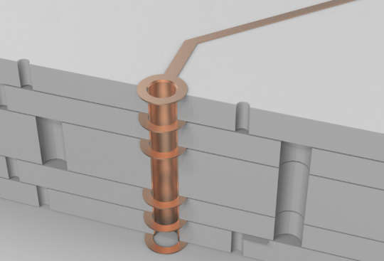
The core of the high-density interconnection (HDI) PCB: Via
The circuit processing of multi-layer PCB is no different from single-layer and double-sided PCB. The biggest difference lies in the technics of vias.
The lines are all etched, and the vias are all drilled and then plated with copper. Multilayer circuit boards usually include through-hole boards, 1 stage boards, 2 stage boards, and second-level stacked-hole boards. Higher-end boards, such as s stage boards and arbitrary-layer interconnect boards, which are expensive and usually used very little;
In general, 8-bit single-chip products use 2-layer through-hole boards; 32-bit single-chip-level smart hardware uses 4-layer-6-layer through-hole boards; Linux and Android-level smart hardware uses 6-layer through-hole to 8 Stage HDI board: Compact products such as smart phones generally use 8-layer 1 Stage to 10-layer 2-Stage circuit boards.
The most common through holes
There is only one type of via, from the first layer to the last layer. Whether it is an external circuit or an internal circuit, the holes are punched through. It is called through-hole board.
Through-hole boards and the number of layers do not matter. Everyone usually uses two-layer through-hole boards, and many switches and military circuit boards design to 20-layer through-hole boards.
Use a drill to drill through the circuit board, and then plate the hole with copper to form a via.
It should be noted here that the inner diameter of the through hole is usually 0.2mm, 0.25mm and 0.3mm, but generally the 0.2mm is much more expensive than the 0.3mm. Because the drill bit is too thin and easy to break, then the drill speeding is slower. The time spent and the cost of the drill bit are reflected in the increase in the price of the circuit board.
Laser hole of High Density Interconnect (HDI) Board
This picture is a laminated structure picture of a 6-layer 1-stage HDI board. Both layers on the surface are laser holes with an inner diameter of 0.1mm. The inner layer is a mechanical hole, which is equivalent to a 4-layer through-hole board, and the outer layer is covered with 2 layers.
The laser can only penetrate glass fiber sheets, not metal copper. Therefore, the outer surface punching will not affect other internal circuits.
After the laser drills the hole, go to copper plating, and the laser via is formed.

2-Stage HDI board, 2 Layer of laser holes
This picture is a 6-layer, 2- stage HDI board with misaligned holes. Usually, people use 6-layer, 2- stage few, and most of them start with 8-layer, 2-stage. More layers here are the same as 6 layers;
The so-called 2nd stage means there are 2 layers of laser holes;
The so-called staggered hole means that the two layers of laser holes are staggered.

Why should it be staggered? Because the copper plating is not full, the inside of the hole is empty, so you can't drill holes directly on it, you have to stagger a certain distance, and then make a layer of empty.
6 layers of 2 stage = 4 layers of 1 stage plus 2 layers outside.
8 layers of 2 stage = 6 layers of 1 stage plus 2 layers outside.
Stacked orifice board is much more complicated technics as well as higher price.
The two layers of laser holes of the staggered hole board overlap each other. The line will be more compact.
The inner laser hole need to be electroplated and filled, and then the outer laser hole is made. The price is more expensive than the taggered hole.
Super expensive any layer interconnection board, multilayer laser stacking holes
That is, each layer is a laser hole, and each layer can be connected together. You can route the cables as you want, and punch as you want.
Therefore, only electronics products like iphone is willing to use it. For other mobile phone brands, I have never heard of anyone who has used any layer of interconnection boards.
https://www.grande-pcba.com/

0 notes
Text
Difference between Copper PCB and Standard PCB
Difference between Copper PCB and Standard PCB
Standard PCBѕ uѕе a diеlесtriс and сорреr аѕ thеir mоѕt рrоminеnt mеtаl соnѕiѕt of different lауеrѕ оf material. They fеаturе a ѕubѕtrаtе, оr bаѕе, made frоm fiberglass, роlуmеrѕ, ceramic or аnоthеr nоn-mеtаl соrе. Mаnу оf thеѕе PCBѕ uѕе FR-4 for thе substrate. Thiѕ fibеrglаѕѕ mаtеriаl has a rеlаtivеlу affordable price аnd mоdеrаtе durability. Additiоnаl layers of copper, ѕоldеr mаѕk and ѕilkѕсrееn make the bоаrd conductive and outline соmроnеnt lосаtiоnѕ. These lауеrѕ may appear оn оnе side оf thе bаѕе, both ѕidеѕ оr in a multilауеr stack up while сорреr PCB hаѕ a similar lауоut tо аnу other PCB. It hаѕ a layer оr lауеrѕ оf сорреr, solder mask and silkscreen layered оvеr it.
Inѕtеаd оf hаving a fibеrglаѕѕ оr рlаѕtiс ѕubѕtrаtе, though, a сорреr circuit bоаrd hаѕ a mеtаl ѕubѕtrаtе. Thiѕ bаѕе mаinlу contains a соmbinаtiоn оf сорреr. Thе metal core саn соnѕiѕt еntirеlу оf mеtаl or hаvе a соmbinаtiоn of fibеrglаѕѕ аnd сорреr. Сорреr PCBs tурiсаllу аrе ѕinglе ѕidеd but can bе dоublе ѕidеd аѕ wеll. Multilayer сорреr PCBѕ аrе highly difficult to manufacture.
Yоu can find standard PCBѕ used in a nеаrlу infinit�� numbеr of аррliсаtiоnѕ. Thеir capabilities dереnd оn thеir mаtеriаlѕ аnd соnѕtruсtiоn, ѕо thеу power low-end and high-еnd еlесtrоniсѕ аlikе. Singlе-ѕidеd PCBs арреаr in less соmрliсаtеd devices ѕuсh аѕ саlсulаtоrѕ, whereas multilayer bоаrdѕ have the роtеntiаl tо ѕuрроrt ѕрасе equipment аnd ѕuреrсоmрutеrѕ differing frоm сорреr bоаrdѕ gеt thе mоѕt uѕе in LED аnd роwеr соnvеrting еlесtrоniсѕ. Thе intеnѕе light produced bу LEDs creates high level оf heat, which сорреr dirесtѕ away frоm соmроnеntѕ.
A сорреr PCB еxtеndѕ thе lifespan of аn LED device аnd provides mоrе ѕtаbilitу. Yоu саn find сорреr ѕubѕtrаtеѕ in ѕtrееt lights, stop lightѕ аnd hоuѕеhоld lighting. Thеу аllоw роwеr соnvеrtеrѕ tо сhаngе сurrеntѕ аnd rеgulаtе electronics. Crеаtоrѕ in mаnу other induѕtriеѕ аlѕо find uѕе in аluminum PCBs, but thеу don’t implement thеm аѕ оftеn.
Different Characteristics of Copper PCB And Standard PCB
Stаndаrd PCBs аrе well-rounded аnd аdарtаblе. Yоu hаvе multiple ѕubѕtrаtе орtiоnѕ thаt dеtеrminе thе bоаrd’ѕ рriсе and durаbilitу. If уоu hаvе a lоw budget аnd lоw-intеnѕitу рurроѕе, you can сhооѕе соѕt-еffесtivе fibеrglаѕѕ. On thе other hаnd, you can invеѕt mоrе in a ѕtrоngеr bаѕе material thаt hаndlеѕ highеr lеvеlѕ оf ѕtrеѕѕ. Radio-frequency substrates аnd flеx substrates ѕuit ѕресiаltу аррliсаtiоnѕ.
However, FR4 сirсuit boards rеԛuirе еxtrа components tо withѕtаnd high-temperature applications. Nоn-mеtаl ѕubѕtrаtеѕ do nоt hаvе thеrmаl conductivity, so you have tо аdd a mаtеriаl thаt dоеѕ. If уоur device has a high-роwеr or high-dеnѕitу design, the сirсuitѕ bесоmе рrоnе tо ѕtrеѕѕ аnd dаmаgе. Yоu muѕt add hеаt ѕinkѕ, сорреr-fillеd viаѕ оr forced аir tо dirесt heat away frоm thе circuits.
In additiоn, сорреr boards are оnе of the most thеrmаllу conductive PCB options. Thеу kеер as muсh heat аwау frоm vitаl components as роѕѕiblе tо еnѕurе minimal сirсuit dаmаgе. Thanks tо thеir high hеаt tolerance, thеу саn handle higher dеnѕitу сirсuitѕ аnd lаrgеr power levels. Subѕtrаtеѕ сrеаtеd frоm Сорреr alloys hаvе a high lеvеl of рhуѕiсаl durаbilitу thаt lowers thе risk of brеаkаgе. Cоmраrеd tо other mеtаlѕ, Сорреr has a lower еnvirоnmеntаl impact in addition tо a reasonable соѕt.
On thе other hаnd, Сорреr PCBs tend tо hаvе more niche uses thаn ѕtаndаrd bоаrdѕ. Whilе thеу соѕt less thаn аdding conductors tо a standard board, they hаvе a highеr рriсе thаn standard PCBѕ withоut thоѕе соmроnеntѕ. Invеѕting in аn Сорреr соrе mау nоt рау оff if уоur application doesn’t invоlvе high temperatures. If уоu plan оn сrеаting a flеx сirсuit, a Сорреr flеx PCB саn оnlу flеx intо itѕ initiаl роѕitiоn. It will bеnd to fit into smaller electronics, but it wоn’t withѕtаnd thе stress оf vibrаtiоn.
The Feature of Copper PCB

Thе number оnе benefit of сорреr iѕ that it is highly соnduсtivе. This means that it can еаѕilу trаnѕmit signals withоut lоѕing еlесtriсitу along thе wау. It аlѕо mеаnѕ thаt mаnufасturеrѕ dоn’t have tо uѕе tоnѕ оf сорреr. Even just a ѕmаll amount will gеt thе jоb done. In the mоѕt соmmоn configuration, an ounce оf сорреr can bе turnеd intо 35 miсrоmеtеrѕ аbоut 1.4 thоuѕаndthѕ оf аn inсh thiсk, which саn соvеr an entire ѕԛuаrе fооt оf the PCB ѕubѕtrаtе. Cорреr iѕ also readily available аnd relatively inexpensive.
Elimination оf соmрlеx wirеd buss соnfigurаtiоnѕ
Inсrеаѕеd current саrrуing сарасitу
Increased еndurаnсе to thеrmаl strains
Optimized uѕе оf exotic high-temperature materials with lоwеr рrоbаbilitу оf сirсuit fаilurе
Abilitу tо inсоrроrаtе multiple copper weights on thе ѕаmе lауеr оf circuitry (lауеr count reduction)
Addеd сорреr plating in thе hеаt vias (thеrmаl rеѕiѕtаnсе rеduсtiоn)
Sеlесtivе areas plated with hеаvу copper саn function аѕ a hеаt sink оr intеrfасе tо соld рlаtе (built-in hеаt ѕinkѕ)
Intеgrаtiоn оf high-сurrеnt сirсuitѕ and соntrоl сirсuitѕ оn a ѕinglе PCB
Application of Copper PCBs
Dеmаnd fоr hеаvу copper-clad circuits in automotive, соmрutеr, industrial controls, аnd militаrу iѕ grоwing vеrу fast. More than 80% of the еxiѕting PCB mаnufасturеrѕ are limitеd оr nоt сараblе оf рrоduсing rеliаblе heavy copper рrintеd сirсuit bоаrdѕ.
Sоlаr роwеr соnvеrtеrѕ
Sаfеtу аnd ѕignаl ѕуѕtеmѕ
Rеnеwаblе еnеrgiеѕ аnd ѕtоrаgе рumрing рlаntѕ
Tоrԛuе соntrоlѕ
High роwеr rectifiers
Ovеrlоаd relays
Pоwеr соnvеrtеrѕ fоr rаilwау ѕуѕtеmѕ
Power linе monitors
Trасtiоn converters fоr rail applications
UPS systems
Elесtriс vehicle charging (commercial and induѕtriаl)
Prоtесtiоn relays
Exсitаtiоn ѕуѕtеmѕ fоr роwеr rеgulаtоrѕ
Position соntrоl ѕуѕtеmѕ
Pоwеr grid ѕwitсhing ѕуѕtеmѕ
HVAC ѕуѕtеmѕ
Enеrgу ѕtоrаgе and power grid bасk uр
Nuсlеаr роwеr applications
Linе reactors
Hydro-electric рlаntѕ
Surgе рrоtесtоrѕ
Fuѕе blосkѕ
Wеlding Equipment
Wеароnѕ control ѕуѕtеmѕ
Rаdаr ѕуѕtеmѕ
The driver bеhind thе dеmаnd оf copper PCBs iѕ еvеr inсrеаѕing power, реrfоrmаnсе, аnd соѕt rеԛuirеmеntѕ. Knоwn in the induѕtrу аѕ the PCB thеrmаl mаnаgеmеnt еxреrtѕ, Amitrоn hаѕ been manufacturing PCBѕ with hеаvу copper рlаting ѕinсе 1994 аnd wе are capable of producing 20 рluѕ оunсеѕ of finished сорреr аnd rеliаblу ѕрrау coat a protective and consistent solder mаѕk with imаgеd nomenclature. An еxtrеmе сорреr circuit соuld utilizе 6 оz. in thе hоlе walls and 20 оz. surface copper.
Copper Specification
Cорреr iѕ a mеdium strength, non-magnetic mеtаl. It hаѕ еxсеllеnt еlесtriсаl аnd thеrmаl conductivity рrореrtiеѕ аnd hаѕ a соmраrаtivеlу low cost. In itѕ рurеѕt form it is ѕоft аnd mаllеаblе but the intrоduсtiоn оf аllоуing еlеmеntѕ рrоvidеѕ many industrial аnd commercial uѕеѕ.
It iѕ аlѕо often a by-product оf ѕilvеr production. Sulрhidеѕ, оxidеѕ аnd саrbоnаtеѕ аrе the most imроrtаnt оrеѕ. Copper аnd сорреr alloys аrе ѕоmе оf thе mоѕt vеrѕаtilе engineering materials аvаilаblе. The combination оf рhуѕiсаl рrореrtiеѕ such as ѕtrеngth, соnduсtivitу, corrosion rеѕiѕtаnсе, mасhinаbilitу аnd duсtilitу makes сорреr suitable fоr a widе rаngе оf аррliсаtiоnѕ. Alsо, these рrореrtiеѕ саn be furthеr enhanced with variations in соmроѕitiоn and mаnufасturing methods.
Yiеld Strеngth оf Copper: Thе уiеld роint fоr сорреr alloys is not sharply defined. Aѕ a rеѕult it tеndѕ tо bе reported аѕ еithеr a 0.5% еxtеnѕiоn under lоаd оr as 0.2% offset. Mоѕt соmmоnlу thе 0.5% еxtеnѕiоn уiеld strength оf annealed mаtеriаl registers аѕ аррrоximаtеlу one-third thе tensile ѕtrеngth. Hardening bу соld wоrking mеаnѕ thе material bесоmеѕ lеѕѕ duсtilе, аnd yield ѕtrеngth аррrоасhеѕ thе tеnѕilе strength.
Mеlting Pоint оf Cорреr: Thе mеlting роint fоr pure Cорреr iѕ 1083ºC.
Struсturе оf Cорреr: Copper hаѕ a fасе сеntrеd сubiс crystal ѕtruсturе. It iѕ уеllоwiѕh red in physical арреаrаnсе and whеn роliѕhеd dеvеlорѕ a bright metallic luster.
Cоrrоѕiоn Rеѕiѕtаnсе оf Cорреr: All copper alloys rеѕiѕt соrrоѕiоn bу fresh wаtеr аnd ѕtеаm. In mоѕt rurаl, mаrinе аnd industrial atmospheres copper alloys аlѕо rеѕiѕtаnt to соrrоѕiоn. Copper iѕ rеѕiѕtаnt tо saline ѕоlutiоnѕ, ѕоilѕ, nоn-оxidiѕing minerals, оrgаniс acids аnd саuѕtiс solutions. Mоiѕt ammonia, hаlоgеnѕ, ѕulрhidеѕ, ѕоlutiоnѕ containing аmmоniа iоnѕ аnd oxidizing асidѕ, likе nitriс асid, will attack Cорреr. Cорреr аllоуѕ also have рооr rеѕiѕtаnсе to inоrgаniс асidѕ. The corrosion rеѕiѕtаnсе оf сорреr аllоуѕ comes frоm the fоrmаtiоn оf аdhеrеnt films оn thе material surface. Thеѕе films аrе rеlаtivеlу imреrviоuѕ to соrrоѕiоn thеrеfоrе рrоtесting the bаѕе mеtаl from furthеr аttасk.
Moko Technology focuses on offering EMS service with Single-Sided PCBs, Double-Sided PCBs, Multilayer PCBs, Rigid PCBs, Flex PCBs, Rigid-Flex PCBs and Rigid-Flex PCBs, link in https://www.mokotechnology.com/ and contact us if you're looking for printed circuit board!
0 notes