#Printed Circuit Board (PCB) Design Market Industry
Text
#Printed Circuit Board (PCB) Design Market#Printed Circuit Board (PCB) Design Market Trends#Printed Circuit Board (PCB) Design Market Growth#Printed Circuit Board (PCB) Design Market Industry#Printed Circuit Board (PCB) Design Market Research
0 notes
Text
Printed Circuit Boards (PCBs) Market Analysis, Key Players, Share Dynamic Demand and Consumption to 2032

The printed circuit boards (PCBs) market refers to the industry involved in the design, production, and sale of PCBs, which are essential components in electronic devices. PCBs provide a platform for interconnecting and supporting various electronic components, such as integrated circuits (ICs), resistors, capacitors, and connectors.
printed circuit board market size is expected to increase USD 3.60 billion by 2032 and Growth Rate from 2023 CAGR of 3.9% Forecast Period 2023 To 2032
Here are some key points about the PCBs market:
Market Size and Growth: The PCBs market has experienced significant growth in recent years. Factors driving this growth include the increasing demand for consumer electronics, telecommunications equipment, automotive electronics, industrial automation, and healthcare devices. The proliferation of smart devices, Internet of Things (IoT) applications, and advancements in technologies like 5G and artificial intelligence also contribute to the expanding PCBs market.
Types of PCBs: PCBs come in different types, including single-sided, double-sided, multi-layered, rigid, flexible, and rigid-flex PCBs. Each type has its specific applications and advantages. For instance, flexible PCBs are used in wearable devices and applications where flexibility and compactness are essential, while multi-layered PCBs are commonly found in complex electronic systems like smartphones and computers.
Manufacturing Process: PCB manufacturing involves several steps, including design, substrate selection, copper etching, solder mask application, and component assembly. The industry has seen advancements in manufacturing techniques such as surface-mount technology (SMT) and advanced packaging, enabling smaller and more complex PCB designs.
Market Players: The PCBs market is highly competitive, with numerous manufacturers operating globally. Some of the key players in the industry include Nippon Mektron Ltd., Unimicron Technology Corp., Zhen Ding Technology Holding Limited, Tripod Technology Corporation, Samsung Electro-Mechanics Co., Ltd., and TTM Technologies, Inc. These companies offer a wide range of PCB products and services to cater to different industries and customer requirements.
Regional Market: Asia-Pacific dominates the global PCBs market, primarily due to the presence of major electronics manufacturing hubs in countries like China, Japan, South Korea, and Taiwan. These countries are known for their strong electronics industry, which drives the demand for PCBs. North America and Europe also contribute significantly to the market due to their established electronics and automotive sectors.
Emerging Trends: The PCBs market is influenced by several emerging trends. These include the miniaturization of electronic devices, the adoption of advanced materials and technologies for higher performance and reliability, the shift towards environmentally friendly and lead-free PCBs, and the growing demand for high-speed and high-frequency PCBs to support advanced applications.
It's worth noting that the PCBs market is subject to various factors, including technological advancements, regulatory requirements, supply chain dynamics, and customer demand. To obtain the most accurate and up-to-date information on the market, it's advisable to refer to industry reports, market research studies, and publications specific to the PCBs market.
I recommend referring to our Stringent datalytics firm, industry publications, and websites that specialize in providing market reports. These sources often offer comprehensive analysis, market trends, growth forecasts, competitive landscape, and other valuable insights into the humidity sensors market.
By visiting our website or contacting us directly, you can explore the availability of specific reports related to the humidity sensors market. These reports often require a purchase or subscription, but we provide comprehensive and in-depth information that can be valuable for businesses, investors, and individuals interested in the market.
Remember to look for recent reports to ensure you have the most current and relevant information.
Click Here, To Get Free Sample Report : https://stringentdatalytics.com/reports/printed-circuit-boards-(pcbs)-market/901/
Market Segmentations:
Global Printed Circuit Boards (PCBs) Market: By Company
• AT&S
• Nippon Mektron
• Unimicron
• Samsung
• Dynamic Electronics
• Daeduck Electronics
• CMK Corporation
• Nan Ya PCB Co.
• TTM Technologies
• Shenzhen Kinwong Electronic
Global Printed Circuit Boards (PCBs) Market: By Type
• Single-sided
• Double-sided
• Multi-layer
Global Printed Circuit Boards (PCBs) Market: By Application
• Consumer Electronics
• Aerospace and Defense
• Automotive
• Healthcare
• Others
Global Printed Circuit Boards (PCBs) Market: Regional Analysis
All the regional segmentation has been studied based on recent and future trends, and the market is forecasted throughout the prediction period. The countries covered in the regional analysis of the Global Printed Circuit Boards (PCBs) market report are U.S., Canada, and Mexico in North America, Germany, France, U.K., Russia, Italy, Spain, Turkey, Netherlands, Switzerland, Belgium, and Rest of Europe in Europe, Singapore, Malaysia, Australia, Thailand, Indonesia, Philippines, China, Japan, India, South Korea, Rest of Asia-Pacific (APAC) in the Asia-Pacific (APAC), Saudi Arabia, U.A.E, South Africa, Egypt, Israel, Rest of Middle East and Africa (MEA) as a part of Middle East and Africa (MEA), and Argentina, Brazil, and Rest of South America as part of South America.
Visit Report Page for More Details: https://stringentdatalytics.com/reports/printed-circuit-boards-(pcbs)-market/901/
Reasons to Purchase Printed Circuit Boards (PCBs) Market Report:
• To obtain insights into industry trends and dynamics, including market size, growth rates, and important factors and difficulties. This study offers insightful information on these topics.
• To identify important participants and rivals: This research studies can assist companies in identifying key participants and rivals in their sector, along with their market share, business plans, and strengths and weaknesses.
• To comprehend consumer behaviour: these research studies can offer insightful information about customer behaviour, including preferences, spending patterns, and demographics.
• To assess market opportunities: These research studies can aid companies in assessing market chances, such as prospective new goods or services, fresh markets, and new trends.
• To make well-informed business decisions: These research reports give companies data-driven insights that they may use to plan their strategy, develop new products, and devise marketing and advertising plans.
In general, market research studies offer companies and organization’s useful data that can aid in making decisions and maintaining competitiveness in their industry. They can offer a strong basis for decision-making, strategy development, and business planning.
Click Here, To Buy Premium Report: https://stringentdatalytics.com/purchase/printed-circuit-boards-(pcbs)-market/901/?license=single
About US:
Stringent Datalytics offers both custom and syndicated market research reports. Custom market research reports are tailored to a specific client's needs and requirements. These reports provide unique insights into a particular industry or market segment and can help businesses make informed decisions about their strategies and operations.
Syndicated market research reports, on the other hand, are pre-existing reports that are available for purchase by multiple clients. These reports are often produced on a regular basis, such as annually or quarterly, and cover a broad range of industries and market segments. Syndicated reports provide clients with insights into industry trends, market sizes, and competitive landscapes. By offering both custom and syndicated reports, Stringent Datalytics can provide clients with a range of market research solutions that can be customized to their specific needs
Contact US:
Stringent Datalytics
Contact No - 91-9763384149
Email Id - [email protected]
Web - https://stringentdatalytics.com/
#Printed Circuit Boards (PCBs) Market Analysis#Key Players#Share Dynamic Demand and Consumption to 2032#The printed circuit boards (PCBs) market refers to the industry involved in the design#production#and sale of PCBs#which are essential components in electronic devices. PCBs provide a platform for interconnecting and supporting various electronic compone#such as integrated circuits (ICs)#resistors#capacitors#and connectors.#printed circuit board market size is expected to increase USD 3.60 billion by 2032 and Growth Rate from 2023 CAGR of 3.9% Forecast Period#Here are some key points about the PCBs market:#1.#Market Size and Growth: The PCBs market has experienced significant growth in recent years. Factors driving this growth include the increas#telecommunications equipment#automotive electronics#industrial automation#and healthcare devices. The proliferation of smart devices#Internet of Things (IoT) applications#and advancements in technologies like 5G and artificial intelligence also contribute to the expanding PCBs market.#2.#Types of PCBs: PCBs come in different types#including single-sided#double-sided#multi-layered#rigid#flexible#and rigid-flex PCBs. Each type has its specific applications and advantages. For instance#flexible PCBs are used in wearable devices and applications where flexibility and compactness are essential
0 notes
Text
Advance your industry with top PCB manufacturers in India
Since the electronics industry is consistently changing, it becomes very important to develop good printed circuit boards. PCBs are the circuitry base of all the electronics, offering the support system needed for the electrical parts to operate effectively.
The industry of manufacturing printed circuit boards has been rapidly growing over the past decade in India. Being one of the most rapidly developing fields in electronics it is to grow further and reach the market value from 3 billion of dollars up to 5 billion of dollars. As a result, it is projected to reach $7 billion by 2025, growing at a compounded rate of 17% annually. 7%.
This rapid expansion is caused by the growing interest in important and growing segments as telecommunication, automotive, healthcare, and consumer electronics segments. The growth of IoT (Internet of Things) and wearable electronics in turn has accelerated this demand, making India a key contributor to the PCB market.

This is actually a move that can revolutionize your industry when you tie up with the top pcb manufacturers in India. These manufacturers provide the quality, technology, and supply chain that your electronics need to perform at their highest level. From this way you can improve reliability of products as well as lower costs and a competitive advantage can be achieved.
Looking for the best way to grow your industry to another level? Partner with the top pcb manufacturers in India today. Epsilon Electronics is delighted to assist you to find the top PCB Manufacturers in India.
#top PCB manufacturers in India#PCB manufacturers in India#ems solution provides#pcb assembly service provider#pcb assembly service provider in gujarat#pcb assembly service provider in india#pcb design company in gujarat#circuit design company in india#ems supplier in india#pcb design company in india
0 notes
Text
Note the Various Benefits of Clone PCB
A clone PCB is a replicated version of an existing printed circuit board (PCB), designed to mimic the layout, components, and functionality of the original PCB. It serves purposes such as backup, legacy support, cost reduction, customization, or reverse engineering. However, creating clone PCBs must be done while considering legal and ethical considerations regarding intellectual property rights.
Sometimes, clone PCBs are created through reverse engineering processes to replicate the functionality of an existing PCB without access to its original design files or documentation. PCB (Printed Circuit Board) reverse engineering is the process of deconstructing and analyzing the design and functionality of a printed circuit board to understand its schematics, layout, and operation.
There are multifaceted benefits of clone PCBs:
Continuity and redundancy - Clone PCBs provide a safety net for businesses by ensuring continuity in production processes. In case the original PCB design becomes unavailable due to damage, loss, or obsolescence, having clone PCBs allows manufacturing to continue without disruptions. This redundancy is crucial for industries where downtime can result in substantial financial losses.
Legacy support and maintenance - Many industries rely on equipment or devices with legacy PCB designs that may no longer be supported by the original manufacturer. Clone PCBs enable the continued operation, maintenance, and repair of such equipment, extending its lifespan and maximizing return on investment. This is particularly important in sectors like aerospace, defense, automotive, and industrial manufacturing, where equipment longevity is paramount.
Cost optimization - Clone PCBs offer opportunities for cost optimization in several ways. By replicating the original PCB design using more readily available or cost-effective components, manufacturers can reduce production costs without sacrificing quality or performance. Additionally, economies of scale can be leveraged when producing clone PCBs in bulk, further driving down per-unit costs.
Flexibility and customization - Clone PCBs can be tailored to meet specific requirements or to incorporate improvements over the original design. Manufacturers can modify aspects such as component selection, layout, or functionality to optimize performance, enhance reliability, or adapt to evolving technological standards. This flexibility enables businesses to stay competitive and responsive to changing market demands.
Reverse engineering and innovation - Clone PCBs support innovation by facilitating reverse engineering efforts. Analyzing and replicating existing PCB designs allows engineers to gain insights into complex electronic systems, identify best practices, and develop new products or technologies based on proven designs. This process fosters creativity, knowledge transfer, and continuous improvement within the industry.
Intellectual property protection - While not directly a benefit, clone PCBs can also help protect intellectual property (IP) by offering a legal and authorized means for manufacturers to reproduce their own designs. This ensures that valuable innovations are safeguarded against unauthorized replication or counterfeiting, preserving the competitive advantage of original equipment manufacturers.
0 notes
Text
Global Top 5 Companies Accounted for 83% of total PCB Software market (QYResearch, 2021)
PCB design software aids electronic engineers in designing layouts for printed circuit boards. Engineers leverage the software to collaborate on the design process, pull previously used circuit board component designs from PCB libraries, and verify circuit schematic designs. PCB design software is most often used by engineering firms and teams that may be involved with product development. PCB design software is often implemented as a part of other design software systems such as product and machine design software and general-purpose CAD software.
The PCB Software industry can be broken down into several segments, On Premises, Cloud Based.
Across the world, the major players cover Siemens, Altium, etc.
According to the new market research report “Global PCB Software Market Report 2023-2029”, published by QYResearch, the global PCB Software market size is projected to reach USD 1.82 billion by 2029, at a CAGR of 8.3% during the forecast period.
Figure. Global PCB Software Market Size (US$ Million), 2018-2029
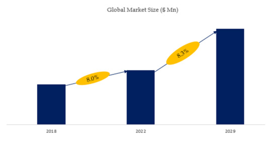
Figure. Global PCB Software Top 13 Players Ranking and Market Share(Based on data of 2021, Continually updated)
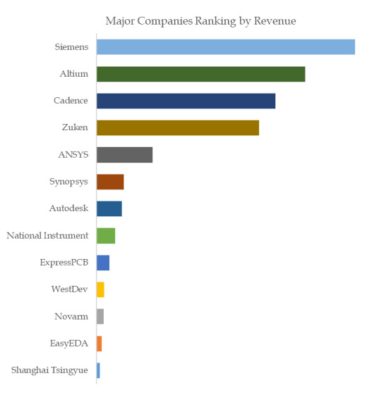
The global key manufacturers of PCB Software include Siemens, Altium, Cadence, Zuken, ANSYS, Synopsys, Autodesk, National Instrument, ExpressPCB, WestDev, etc. In 2021, the global top five players had a share approximately 83.0% in terms of revenue.
About QYResearch
QYResearch founded in California, USA in 2007.It is a leading global market research and consulting company. With over 16 years’ experience and professional research team in various cities over the world QY Research focuses on management consulting, database and seminar services, IPO consulting, industry chain research and customized research to help our clients in providing non-linear revenue model and make them successful. We are globally recognized for our expansive portfolio of services, good corporate citizenship, and our strong commitment to sustainability. Up to now, we have cooperated with more than 60,000 clients across five continents. Let’s work closely with you and build a bold and better future.
QYResearch is a world-renowned large-scale consulting company. The industry covers various high-tech industry chain market segments, spanning the semiconductor industry chain (semiconductor equipment and parts, semiconductor materials, ICs, Foundry, packaging and testing, discrete devices, sensors, optoelectronic devices), photovoltaic industry chain (equipment, cells, modules, auxiliary material brackets, inverters, power station terminals), new energy automobile industry chain (batteries and materials, auto parts, batteries, motors, electronic control, automotive semiconductors, etc.), communication industry chain (communication system equipment, terminal equipment, electronic components, RF front-end, optical modules, 4G/5G/6G, broadband, IoT, digital economy, AI), advanced materials industry Chain (metal materials, polymer materials, ceramic materials, nano materials, etc.), machinery manufacturing industry chain (CNC machine tools, construction machinery, electrical machinery, 3C automation, industrial robots, lasers, industrial control, drones), food, beverages and pharmaceuticals, medical equipment, agriculture, etc.
For more information, please contact the following e-mail address:
Email: [email protected]
Website: https://www.qyresearch.com
0 notes
Text
Advanced Materials for Electronics is Projected to Grow at a 7.4% CAGR between 2022 and 2031
The Advanced Materials for Electronics Market is predicted to reach US$ 57.8 billion by 2031. According to market forecasts, the market is expected to grow at a CAGR of 7.4% through 2031.
Electronics that are printed and flexible continue to grow at a fast rate. Along the value chain, energy and resource efficiency can be significantly increased through new technological approaches to both production and product design.
Electronics are undergoing constant reorganization to meet changing consumer demands, which results in continuously evolving technologies, materials, and business models. Innovations in the technology industry have been stimulated by the growing need for miniaturized and improved capacity computers and networks, faster data transmission speeds, and most importantly, sustainable technologies.
For instance, a new high-speed broadband standard protocol for digital subscriber lines (DSL) was approved by the International Telecommunication Union (ITU) in December 2014. It is referred to as Gaits for local loops under 500 meters that support uploads and downloads at 150 Mb/s to 2 Gb/s. A local loop's length determines how fast Gaits can transmit data. It is mandatory in Gaits to have an asymmetry ratio of 90/10 to 50/50 between downstream and upstream
Download Sample Copy with Graphs & List of Figures: https://www.transparencymarketresearch.com/sample/sample.php?flag=S&rep_id=85652
Market Segmentation
The advanced materials for electronics market can be segmented by service type, sourcing type, application, industry vertical, and region.
By Service Type
Design and Consulting
Integration and Implementation
Maintenance and Support
By Sourcing Type
In-house
Outsourced
By Application
Semiconductor Devices
Printed Circuit Boards (PCBs)
Display Panels
Batteries and Energy Storage
By Industry Vertical
Consumer Electronics
Automotive
Telecommunications
Healthcare
Energy and Power
By Region
North America
Europe
Asia-Pacific
Latin America
Middle East and Africa
Regional Analysis
North America: Dominates the market due to the presence of major semiconductor companies and substantial investments in R&D.
Europe: Shows significant growth driven by the automotive sector, particularly in EVs.
Asia-Pacific: Expected to witness the fastest growth owing to the large consumer electronics market and manufacturing hub in countries like China, Japan, and South Korea.
Latin America and Middle East & Africa: Emerging markets with growing investments in technology infrastructure and renewable energy projects.
Market Drivers and Challenges
Drivers:
Technological Advancements: Innovations in semiconductor and nanotechnology drive the demand for advanced materials.
Growing Consumer Electronics Market: Increased adoption of smartphones, tablets, and wearable devices.
Electric Vehicles and Renewable Energy: Rising demand for EVs and renewable energy solutions, which require advanced battery materials and energy storage systems.
Challenges:
High Production Costs: The advanced materials often require complex and costly manufacturing processes.
Supply Chain Issues: Dependency on specific raw materials which might be geographically concentrated or scarce.
Regulatory Hurdles: Stringent environmental regulations regarding material production and disposal.
Market Trends
Miniaturization of Electronic Devices: Increasing demand for smaller, lighter, and more efficient electronic components.
Development of Flexible and Wearable Electronics: Surge in demand for materials that are flexible and can be integrated into wearable technology.
Sustainability: Focus on environmentally friendly materials and sustainable manufacturing processes.
Future Outlook
The future of the advanced materials for electronics market looks promising with continuous innovations and increasing integration of these materials in various high-tech applications. The push towards 5G technology, AI, and IoT will further amplify the demand for advanced electronic materials. Additionally, the evolution of the EV market and renewable energy solutions will continue to create substantial growth opportunities.
Key Market Study Points
Detailed analysis of market size and growth projections.
Comprehensive segmentation analysis to understand market dynamics.
Regional performance and growth prospects.
Identification of key market drivers, challenges, and trends.
Future outlook and strategic recommendations for market participants.
Competitive Landscape
The market is characterized by intense competition with several key players investing heavily in R&D to gain a competitive edge. Major companies include BASF SE, DowDuPont Inc., Samsung SDI, LG Chem, and 3M. These players focus on strategic partnerships, mergers, acquisitions, and new product developments to expand their market presence.
Buy this Premium Research Report | Immediate Delivery Available: https://www.transparencymarketresearch.com/checkout.php?rep_id=85652<ype=S
Recent Developments
BASF SE recently announced the development of a new line of conductive polymers for flexible electronics.
Samsung SDI expanded its production capacity for advanced battery materials to meet the growing demand from the EV market.
3M launched a new range of high-temperature resistant adhesives for semiconductor applications.
About Transparency Market Research
Transparency Market Research, a global market research company registered at Wilmington, Delaware, United States, provides custom research and consulting services. Our exclusive blend of quantitative forecasting and trends analysis provides forward-looking insights for thousands of decision makers. Our experienced team of Analysts, Researchers, and Consultants use proprietary data sources and various tools & techniques to gather and analyses information.
Our data repository is continuously updated and revised by a team of research experts, so that it always reflects the latest trends and information. With a broad research and analysis capability, Transparency Market Research employs rigorous primary and secondary research techniques in developing distinctive data sets and research material for business reports.
Contact:
Transparency Market Research Inc.
CORPORATE HEADQUARTER DOWNTOWN,
1000 N. West Street,
Suite 1200, Wilmington, Delaware 19801 USA
Tel: +1-518-618-1030
USA – Canada Toll Free: 866-552-3453
Website: https://www.transparencymarketresearch.com
0 notes
Text
The Rise of Drone PCB Technology in China: An Aerial Revolution

Over the last decade, China's drone industry has seen explosive growth, emerging as a global leader. At the heart of drone technology lies its intricate electronic systems, with Printed Circuit Boards (PCB) playing an indispensable role. China's advancements in drone PCB technology not only enhance the operational capabilities of drones but also position the country at the forefront of the aerial technology sector.
Key Developments in China's Drone PCB Technology
Drone PCBs in China have evolved significantly, driven by both demand and technological innovation. These circuit boards are designed to be lightweight yet robust, capable of withstanding various environmental challenges while maintaining functionality. The integration of high-density interconnect (HDI) technology is a notable advancement. HDI PCBs allow for finer lines and spaces, smaller vias, and higher connection pad densities, which are crucial for the miniaturization of drones and enhancement of their functionality.
Another significant advancement is the use of flexible PCBs. These are particularly beneficial for drones as they conform to the contours of uniquely shaped devices, reducing weight and improving reliability. Flex PCBs are integral in drones, facilitating complex connections between different sections of the drone without sacrificing performance.
Impact on Commercial and Military Applications
China's drone technology is not limited to consumer applications but extends to significant military and commercial uses. In commercial sectors, drones equipped with advanced PCBs are used for agricultural monitoring, aerial photography, and logistics. These drones require highly reliable PCBs to perform tasks such as real-time data processing, navigation, and autonomous operation.
Military drones, on the other hand, demand even more from their PCBs. They must operate under extreme conditions and often carry additional payloads such as communication hardware, sensors, and sometimes weaponry. The reliability of these PCBs is critical, as they must ensure the drone's performance in critical missions.
Challenges and Innovations
Despite these advancements, the drone PCB manufacturing sector in China faces several challenges. One of the primary concerns is the need for continual innovation to keep up with the rapidly evolving drone technologies. This requires constant research and development efforts to devise more efficient, durable, and smaller PCBs that fit the new generations of drones.
Another challenge is environmental sustainability. The PCB manufacturing process can be resource-intensive and environmentally taxing. Addressing these concerns, many Chinese PCB manufacturers are increasingly turning towards more sustainable manufacturing processes and materials, which not only reduce the environmental impact but also cater to the global demand for greener electronics.
Collaboration and Global Influence
China's drone PCB industry is not operating in isolation but is part of a larger global ecosystem. There is extensive collaboration between Chinese PCB manufacturers and global technology firms, enhancing the overall quality and capabilities of drone technologies. These collaborations help set international standards for drone PCBs, which, in turn, influence global market trends.
China's influence in the drone sector also extends to its role in setting global regulatory standards. As a leading market player, the policies and standards set in China have a cascading effect, influencing how drones are manufactured and used worldwide.
The Future of Drone PCBs in China
Looking forward, the future of drone PCBs in China is tied to the broader trends in technology such as AI and IoT. Integration of AI allows drones to perform more complex tasks autonomously, such as predictive maintenance and threat assessment in military applications. IoT integration, on the other hand, enables better connectivity and control, essential for managing fleets of drones used in logistics or agricultural monitoring.
Moreover, as 5G technology becomes more widespread, the capabilities of drones are expected to expand further. The ultra-low latency and high-speed connectivity offered by 5G will enhance the real-time data transmission abilities of drones, opening up new possibilities for their application.
Conclusion
China’s rapid advancements in drone PCB technology showcase its capacity to lead in high-tech industries. As the country continues to innovate and push the boundaries of what drones can achieve, the global impact of its developments will undoubtedly continue to grow. The integration of cutting-edge technologies into drone PCBs not only transforms the landscape of the drone industry but also sets the stage for the next era of aerial innovation.
0 notes
Text
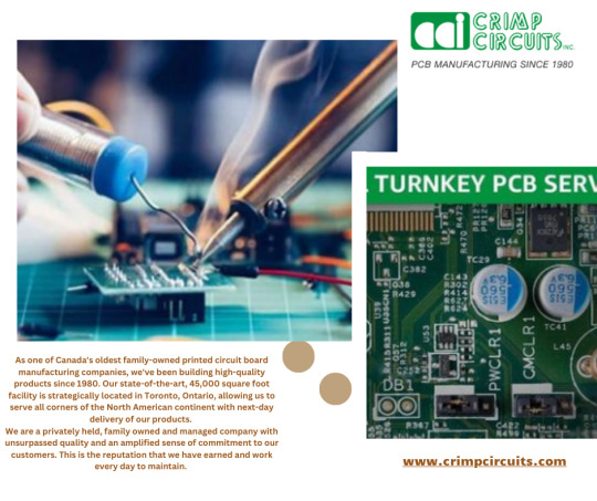
Unveiling the Excellence of PCB Manufacturing in Toronto with Crimp Circuits
Introduction: In the bustling hub of technological innovation that is Toronto, Canada, Crimp Circuits stands as a beacon of excellence in the realm of PCB manufacturing. With a rich history spanning over four decades, Crimp Circuits has established itself as a leader in the industry, delivering cutting-edge solutions to clients across a diverse range of sectors. In this blog, we'll delve into the world of PCB manufacturing in Toronto and shed light on how Crimp Circuits continues to set the standard for excellence in the field.
A Legacy of Innovation: Since our inception, Crimp Circuits has been at the forefront of technological innovation, pushing the boundaries of what's possible in PCB manufacturing. Our state-of-the-art facility, located in the heart of Toronto, boasts advanced equipment, experienced personnel, and a commitment to excellence that sets us apart from the competition. From concept to completion, we pride ourselves on delivering superior PCB solutions that meet and exceed the expectations of our clients.
Precision Engineering and Design: At Crimp Circuits, precision is our watchword. Our team of skilled engineers and designers leverage the latest technology, including Eagle software, to create PCB designs that are optimized for performance, reliability, and efficiency. Whether it's a simple two-layer board or a complex multilayered design, we have the expertise and experience to bring your vision to life with unparalleled precision and accuracy.
Diverse Range of Offerings: Crimp Circuits offers a comprehensive suite of PCB manufacturing services to meet the diverse needs of our clients. From printed circuit board design and prototyping to full-scale production and assembly, we have the capabilities and resources to handle projects of any size or complexity. Whether you're a startup looking to bring a new product to market or a large corporation in need of high-volume production, Crimp Circuits has you covered.
Quality Assurance and Compliance: Quality is ingrained in everything we do at Crimp Circuits. We adhere to stringent quality control measures at every stage of the manufacturing process to ensure that our clients receive PCBs of the highest quality and reliability. Additionally, we maintain compliance with industry standards and regulations, giving our clients peace of mind knowing that their products meet all necessary requirements.
Customer-Centric Approach: At Crimp Circuits, we understand that our success is directly tied to the success of our clients. That's why we take a customer-centric approach to every project, prioritizing open communication, collaboration, and responsiveness. We work closely with our clients to understand their unique needs and requirements, ensuring that we deliver solutions that not only meet but exceed their expectations.
Conclusion: In conclusion, PCB manufacturing in Toronto is synonymous with excellence, innovation, and reliability, thanks to companies like Crimp Circuits. With our state-of-the-art facilities, experienced team, and commitment to quality, we continue to set the standard for PCB manufacturing in the region and beyond. Contact us today to learn more about how Crimp Circuits can meet your PCB manufacturing needs.For more details visit our website: www.crimpcircuits.com
#pcb manufacturing toronto#printed circuit board design#metal clad pcb#printed circuits#rigid flex pcb#full turnkey pcb services#turnkey pcb services#pcb parts#eagle software#pcb designing#flexible pcb#pcb assembly#printed circuit board manufacturers#pcb manufacturers in canada#circuit board manufacturers in canada#pcb quote#pcb prototype services in canada
0 notes
Text
Decoding PCBA Board Manufacture: A Roadmap to Efficient Production
PCBA (Printed Circuit Board Assembly) board manufacture stands as a pivotal stage in the journey from electronic concept to tangible product. This blog offers a detailed roadmap, guiding both novices and seasoned professionals through the multifaceted process of PCBA board manufacture.
The journey initiates with an elucidation of PCBA board components, ranging from basic resistors to intricate microprocessors. Understanding the role and compatibility of each component is paramount in crafting a functional and efficient board.
Subsequently, the blog navigates through the intricacies of PCB fabrication, encompassing design optimization, material selection, and fabrication techniques. Through insights into surface finishes, layer stackups, and trace routing, readers will grasp the fundamentals necessary for creating robust and reliable PCBs.
The narrative then transitions to the assembly phase, shedding light on component placement, soldering methodologies, and quality assurance protocols. From manual soldering to automated pick-and-place systems, readers will gain insight into the diverse assembly techniques and their respective advantages.
Moreover, the blog addresses the significance of thorough testing and inspection procedures to identify and rectify potential defects before the final product reaches the market. Topics such as in-circuit testing, functional testing, and quality control standards underscore the importance of delivering reliable and high-performance PCBAs.
In conclusion, "Decoding PCBA Board Manufacture" serves as a comprehensive guide for navigating the complexities of PCB assembly manufacturing. By leveraging the insights and best practices shared in this blog, electronics enthusiasts and industry professionals alike can streamline their manufacturing processes, ultimately fostering innovation and excellence in the realm of electronic design and production.
#pcb circuit#fr4 pcb#pcb factory#circuit board#led circuit board#flex pcb#pcb assembly#aluminum pcb#fpc#ems pcba
0 notes
Text
What is Electronic Design Automation (EDA)

Electronic Design Automation (EDA) technologies are critical in the fast-paced field of electronics, where innovation is the key to success and Understanding EDA is essential for students interested in pursuing careers in electrical engineering and industrial automation also we will dissect the complexity of Electronic Design Automation, investigating its relevance, applicability, and critical position in the specialized subject of Industrial Automation within Electrical Engineering schools.
What Is Electronic Design Automation (EDA)?
Electronic Design Automation refers to a category of software tools used for designing electronic systems such as integrated circuits and printed circuit boards. EDA tools facilitate the design, analysis, and simulation of electronic systems, ensuring efficiency and accuracy in the development process.
Significance Of EDA In Electrical Engineering
Streamlining the Design Process:
EDA tools streamline the design process by providing a virtual platform where engineers can create, test, and modify their designs This iterative process enhances creativity and innovation.
Cost Efficiency:
By identifying errors and optimizing designs before physical prototypes are created, EDA tools significantly reduce development costs, also this cost efficiency is paramount, especially in large-scale industrial projects.
Simulation and Analysis:
EDA tools enable engineers to simulate and analyze the behavior of electronic circuits under different conditions as well as this virtual testing ensures that the final product meets the required specifications and standards.
Time-Saving:
In the competitive world of technology, time-to-market is crucial. EDA tools accelerate the design process, allowing engineers to meet tight deadlines without compromising on quality.
Applications of EDA:
Integrated Circuit (IC) Design:
EDA tools are extensively used in IC design, enabling engineers to create complex circuits with millions of transistors However, these circuits power various electronic devices, from smartphones to computers.
Printed Circuit Board (PCB) Design:
In PCB design, EDA tools assist engineers in creating the layout of electronic components on a board, So this layout is fundamental for the proper functioning of devices like laptops, televisions, and medical equipment.
FPGA (Field-Programmable Gate Array) Design:
FPGAs are versatile chips that can be programmed to perform specific tasks also EDA tools aid engineers in designing and programming FPGAs for applications in telecommunications, automotive, and aerospace industries.
Why Specialize In Industrial Automation?
Industrial Automation is the backbone of modern manufacturing processes specializing in this field, students gain expertise in automating industrial processes, leading to increased efficiency, reduced operational costs, and enhanced productivity.
Role of EDA in Industrial Automation:
In the Industrial Automation specialization program, students learn to leverage EDA tools to design electronic systems for automation, also students can understand how EDA contributes to the development of smart sensors, control systems, and robotic applications, essential components of modern industrial setups.
A strong grasp of Electronic Design Automation is essential in the ever-changing field of electrical engineering. EDA tools are the foundations of innovation, from envisioning complicated integrated circuits to optimizing PCB layouts and powering industrial automation. To make meaningful progress in the field of Industrial Automation, aspiring engineers must understand the complexities of EDA.
Students set the path for groundbreaking technological improvements by adopting the information and skills taught by EDA tools Remember that Electronic Design Automation is your passport to a future filled with invention, creativity, and endless possibilities as you start on your journey into the world of Electrical Engineering and Industrial Automation.
Arya College of Engineering & I.T. has a B.E. in Electronics & Communications Engineering (ECE) program is a cutting-edge, four-year undergraduate course meticulously designed in consultation with the electronics industry also with a focus on emerging technologies such as IoT, VLSI, and Embedded Systems, the curriculum provides a strong foundation in core electronics concepts while allowing students to specialize according to their interests.
The program offers invaluable experiential learning opportunities through collaborations with industry leaders like Nvidia and Texas Instruments, enabling students to work with state-of-the-art electronic training equipment, and a mandatory 6-month to 1-year industrial training stint and placement opportunities in Fortune 500 companies to ensure that graduates are not only academically adept but also industry-ready. The program equips students to pursue diverse career paths, from software analysis and network planning to research and development, in the rapidly evolving fields of electronics and communications.
Arya College of Engineering & I.T. ECE program stands as a beacon for aspiring engineers, providing a unique blend of theoretical knowledge and practical expertise. With a focus on hands-on learning, industry-oriented specializations, and world-class facilities, Arya prepares students to be the next generation of innovators and problem solvers. By choosing Arya, students embark on a transformative journey that not only hones their technical skills but also nurtures their entrepreneurial spirit, ensuring they are well-equipped to make a significant impact in the dynamic world of technology
Source: Click Here
#best btech college in jaipur#best engineering college in jaipur#best btech college in rajasthan#best private engineering college in jaipur#b tech electrical in jaipur#best engineering college in rajasthan#top engineering college in jaipur
0 notes
Text
The Gap Explore our PCB Reverse Engineering and Cloning Solutions
In today's fast-paced technological landscape, staying ahead of the curve is paramount for businesses aiming to innovate and thrive. One crucial aspect of this endeavor lies in printed circuit boards (PCBs), the backbone of electronic devices. PCBs serve as the foundation for the functionality and performance of countless electronic products, ranging from consumer electronics to industrial machinery.
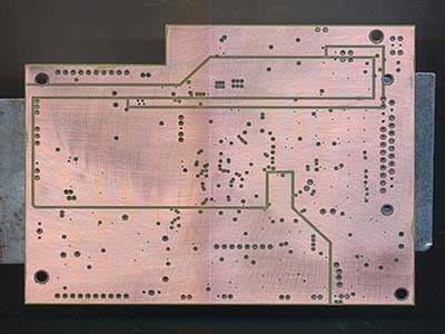
However, for many businesses, accessing and modifying existing PCB designs or replicating them for their own purposes can present significant challenges. This is where PCB reverse engineering and cloning services come into play, offering a pathway to unlocking innovation and accelerating product development cycles.
Understanding PCB Reverse Engineering:
PCB reverse engineering is a meticulous process that involves dissecting and analyzing an existing printed circuit board to understand its design, functionality, and components. This involves a combination of technical expertise, advanced tools, and a keen understanding of electronic systems.
The primary objective of PCB reverse engineering is to extract the schematic diagram, layout, and component information from the original board without access to its design files or documentation. This information serves as the blueprint for further analysis, modification, or replication of the PCB.
The Importance of PCB Cloning Services:
PCB cloning, a subset of reverse engineering, entails replicating an existing PCB design without the need for original design files or documentation. This service is invaluable for businesses seeking to reproduce obsolete or discontinued PCBs, upgrade outdated designs, or enhance the performance of existing products.
By leveraging PCB cloning services, businesses can:
Achieve Cost Efficiency: Creating new PCB designs from scratch can be time-consuming and expensive. PCB cloning offers a cost-effective alternative by leveraging existing designs as a foundation, reducing development time and expenses.
Maintain Legacy Systems: In industries where legacy equipment is prevalent, accessing replacement parts or upgrading outdated systems can be challenging. PCB cloning enables businesses to extend the lifespan of legacy systems by reproducing obsolete or hard-to-find PCBs.
Accelerate Time-to-Market: Time is of the essence in competitive markets. PCB cloning services expedite the product development process by providing ready-made solutions based on existing designs, allowing businesses to bring new products to market faster.
Enhance Product Performance: Through reverse engineering and analysis, PCB cloning services offer opportunities for optimizing existing designs, improving functionality, and integrating advanced features to enhance product performance.
Our Commitment to Excellence:
At PCB reverse engineering, we specialize in providing comprehensive PCB reverse engineering and cloning services tailored to meet the unique needs of our clients. With a team of experienced engineers and state-of-the-art facilities, we offer the following key capabilities:
Advanced Reverse Engineering Techniques: Our engineers are proficient in utilizing cutting-edge tools and methodologies to reverse engineer even the most complex PCB designs accurately. From schematic capture to layout extraction, we ensure precision and reliability throughout the process.
Customized Cloning Solutions: Whether you require exact replicas of existing PCBs or modifications to enhance performance, we tailor our cloning services to align with your specific requirements. Our team collaborates closely with clients to understand their objectives and deliver customized solutions that exceed expectations.
Comprehensive Component Analysis: Component sourcing plays a critical role in PCB cloning projects. We conduct thorough component analysis to identify and source compatible components, ensuring seamless integration and optimal performance of cloned PCBs.
Quality Assurance: Quality is at the forefront of everything we do. We adhere to stringent quality control measures throughout the PCB cloning process, from initial analysis to final production. Our commitment to quality ensures that every cloned PCB meets the highest standards of performance and reliability.
Unlocking Innovation Together:
At PCB reverse engineering, we believe that innovation knows no bounds. Whether you're a startup looking to disrupt the market or an established enterprise seeking to stay ahead of the competition, our PCB reverse engineering and cloning services provide the foundation for your success.
By partnering with us, you gain access to a wealth of expertise, resources, and support needed to turn your vision into reality. From concept to production, we're with you every step of the way, empowering you to unleash the full potential of your electronic products.
Get Started Today: Ready to take your PCB design to the next level? Contact us today to learn more about our PCB reverse engineering and PCB cloning services and discover how we can help you achieve your goals. Together, let's unlock innovation and shape the future of electronics.
#cloning services provide#PCB reverse engineering#PCB cloning services#PCB designs#Electronic System
0 notes
Text
The Role of PCB Test Fixtures in Waterloo and Montreal
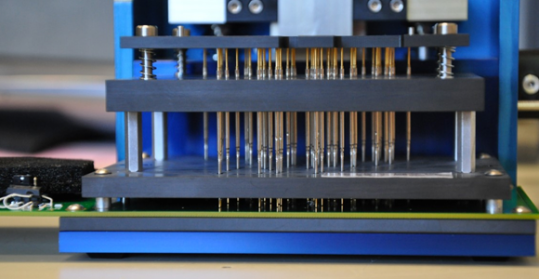
In the vibrant tech hubs of Waterloo and Montreal, where innovation and technology intersect, the demand for efficient electronics testing solutions is ever-present. PCB (Printed Circuit Board) test fixtures serve as indispensable tools for verifying the functionality and reliability of electronic components and assemblies. Let's delve into how PCB Test Fixture Waterloo and PCB Test Fixture Montreal play a crucial role in streamlining testing processes and driving technological advancement in these dynamic cities.
A PCB Test Fixture Waterloo, also known as a test jig or test rig, is a specialized tool designed to facilitate the testing of electronic circuits, assemblies, and devices. It consists of a custom-designed interface that securely holds the PCB in place and provides access to test points, connectors, and components for electrical testing.
PCB Test Fixture Waterloo are engineered to accommodate a wide range of PCB designs and configurations, from simple single-layer boards to complex multi-layer assemblies. They are essential for conducting functional tests, continuity checks, and performance evaluations to ensure the quality and reliability of electronic products before they reach the market.
The integration of advanced technologies such as automated test equipment (ATE), boundary scan testing, and in-circuit testing (ICT) further enhances the capabilities of PCB Test Fixture Waterloo, enabling faster and more comprehensive testing procedures.
In Waterloo, renowned for its vibrant tech ecosystem and world-class research institutions, PCB Test Fixture Waterloo play a pivotal role in accelerating product development cycles and driving innovation. Local companies and startups leverage these fixtures to validate prototypes, refine designs, and conduct rigorous testing to meet stringent quality standards.
With access to cutting-edge technologies and expertise in electronics design and manufacturing, PCB Test Fixture Montreal providers offer tailored solutions to address the diverse needs of clients across industries. Whether it's testing automotive electronics, medical devices, telecommunications equipment, or consumer electronics, these fixtures enable companies to achieve faster time-to-market and maintain a competitive edge in their respective markets.
In Montreal, a hub of technological excellence and innovation, PCB Test Fixture Montreal play an integral role in supporting the city's thriving aerospace, automotive, and electronics industries. Local companies and research institutions rely on these fixtures to validate designs, conduct reliability testing, and ensure compliance with industry regulations and standards.
PCB Test Fixture Montreal leverage their expertise in electronics engineering and manufacturing to deliver high-quality, reliable solutions tailored to the unique requirements of each client. Whether it's testing avionics systems, power electronics, or IoT devices, these fixtures enable companies to achieve optimal performance and reliability in their products.
Collaboration between PCB Test Fixture Waterloo and PCB Test Fixture Montreal, technology companies, and academic institutions drives innovation and technological advancement. By sharing knowledge, resources, and best practices, stakeholders in these cities contribute to the development of cutting-edge testing solutions that push the boundaries of what's possible in electronics design and manufacturing.
PCB Test Fixture Waterloo and PCB Test Fixture Montreal play a critical role in the electronics testing process, enabling companies in Waterloo and Montreal to validate designs, ensure quality, and drive technological advancement. By leveraging advanced technologies and expertise, these fixtures streamline testing procedures, accelerate product development cycles, and maintain the high standards of quality and reliability expected in today's competitive markets. As Waterloo and Montreal continue to thrive as centers of innovation and excellence, PCB Test Fixture Waterloo and PCB Test Fixture Montreal will remain essential tools for advancing technology and driving progress across industries.
0 notes
Text
Quick Turn PCB Services: Empowering Innovation in Boston's Tech Hub

In the vibrant tech ecosystem of Boston, where innovation thrives and breakthroughs are a daily occurrence, the need for rapid prototyping and agile manufacturing solutions is paramount. Quick Turn PCB Boston and Quick Turn PCB Assembly, play a pivotal role in accelerating product development cycles, enabling entrepreneurs, startups, and established companies alike to bring their ideas to market faster than ever before.
A Printed Circuit Board (PCB) serves as the foundation of nearly all electronic devices, providing a platform for connecting and mounting various electronic components. Quick Turn PCB Boston specialize in expediting the fabrication of custom-designed PCBs, offering rapid prototyping and short lead times to meet the demands of fast-paced development cycles.
Quick Turn PCB Boston leverage advanced manufacturing technologies and streamlined processes to deliver high-quality PCBs with unmatched speed and precision. Whether it's a simple single-layer board or a complex multi-layer design, these services prioritize efficiency and reliability, allowing innovators to iterate rapidly and refine their designs with confidence.
While rapid PCB fabrication is essential, the assembly of electronic components onto the board is equally critical in the product development process. Quick Turn PCB Assembly services complement rapid prototyping by offering fast and efficient assembly solutions tailored to the specific needs of each project.
In Boston's tech hub, Quick Turn PCB Assembly services excel in agility and responsiveness, leveraging state-of-the-art equipment and skilled technicians to assemble PCBs quickly and accurately. From surface mount technology (SMT) to through-hole assembly, these services accommodate diverse component types and assembly requirements, ensuring compatibility with a wide range of electronic applications.
The integration of Quick Turn PCB Assembly with rapid prototyping services streamlines the product development workflow, allowing designers and engineers to validate their designs in real-world conditions more rapidly. By shortening the time from concept to functional prototype, quick turn PCB assembly accelerates time-to-market and provides a competitive edge in today's fast-paced business landscape.
The benefits of Quick Turn PCB Boston and Quick Turn PCB Assembly extend far beyond speed and efficiency; they are enablers of innovation, driving progress and breakthroughs across industries. In Boston, where technological advancement is a way of life, these services serve as catalysts for creativity and ingenuity, fueling the next generation of groundbreaking products and solutions.
Whether it's developing cutting-edge medical devices, pioneering renewable energy technologies, or revolutionizing communication systems, Quick Turn PCB Boston and Quick Turn PCB Assembly play a pivotal role in transforming ideas into reality. By providing rapid prototyping and assembly solutions tailored to the unique needs of Boston's diverse tech community, these services empower innovators to push the boundaries of what's possible and shape the future of technology.
In the dynamic landscape of Boston's tech scene, Quick Turn PCB Boston and Quick Turn PCB Assembly are indispensable partners in the journey from concept to market. With their ability to deliver rapid prototyping and assembly solutions with unmatched speed and precision, these services fuel innovation, accelerate time-to-market, and drive progress across industries. As Boston continues to lead the way in technological innovation, quick turn PCB services will remain essential tools for turning ideas into reality and shaping the future of technology.
0 notes
Text
Insights of PCB Reverse Engineering Services Highlighting Its Benefits
PCB reverse engineering services or Printed Circuit boards have emerged as a crucial solution in the world of electronics. Essentially, it involves dissecting and analyzing the design and functionality of a PCB to reconstruct its schematics, layout, and components. This carefully designed process enables engineers to comprehend the intricacies of existing circuit boards without the aid of original documentation. While it may sound like a daunting task, SZOROD has made it easy for you! Delve into the world of PCB reverse engineering services including the benefits it offers that are substantial and multifaceted.
Unraveling Design Mysteries for Innovation
One of the primary advantages of our PCB reverse engineering services lies in its ability to create innovation. By unraveling the design mysteries of legacy PCBs or proprietary systems, our engineers gain invaluable insights into the underlying technology. This knowledge serves as a springboard for innovation, allowing us to develop enhanced versions of existing products or devise entirely new solutions based on proven designs. Whether it's optimizing performance, reducing costs, or adding new features, SZOROD empowers your businesses to stay competitive in dynamic markets.
Facilitating Legacy Product Support and Maintenance
In today's technological landscape, obsolescence is a constant challenge, particularly for legacy products. PCB reverse engineering services by SZOROD offer a lifeline in such scenarios by enabling the recreation of obsolete or discontinued circuit boards. This not only ensures continuity in product support but also extends the lifespan of your valuable assets, which ultimately saves time and resources in the long run.
Enhancing Supply Chain Flexibility and Resilience
The global supply chain is susceptible to various disruptions, ranging from component shortages to geopolitical tensions. In such volatile environments, having alternatives is paramount for business continuity. Our PCB reverse engineering services provide a strategic advantage by offering an alternative source for critical components or assemblies. By our reverse engineering PCBs, you can mitigate supply chain risks, reduce dependency on single suppliers, and maintain production continuity even in the face of unforeseen challenges.
Enabling Intellectual Property Protection and Compliance
Protecting intellectual property (IP) is a top priority for companies across industries. In an interconnected world, safeguarding proprietary designs can be challenging, especially when outsourcing manufacturing or collaborating with third-party vendors. SZOROD’s PCB reverse engineering services play a pivotal role in IP protection by enabling your company to assess the security of its designs and detect any potential vulnerabilities. Also, our reverse engineering can aid in ensuring compliance with industry standards and regulations, thus mitigating legal risks and liabilities.
Driving Cost-Efficiency and Time Savings
Last but not least, our PCB reverse engineering services offer significant cost-efficiency and time-saving benefits. Instead of starting from scratch, which involves extensive research, prototyping, and testing, our services will allow your company to leverage existing designs as a foundation. This streamlined approach reduces development cycles, accelerates time-to-market, and ultimately lowers overall project costs.
1 note
·
View note
Text
SMD Thick Film Resistor, Global Market Size Forecast, Top 14 Players Rank and Market Share
SMD Thick Film Resistor Market Summary
Surface Mount Device (SMD) thick film resistors are electronic components used in circuitry to control the flow of electric current. These resistors are made using a thick film deposition process, where a resistive paste is printed onto a ceramic substrate and then baked to form the resistive element. SMD thick film resistors are designed for surface mounting onto printed circuit boards (PCBs), offering advantages like space efficiency, ease of automated assembly, and good stability under various operating conditions. They come in various sizes and power ratings, catering to different application needs. The "thick film" aspect refers to the thicker layer of resistive material compared to thin film resistors, providing different electrical and thermal properties.
Figure. SMD Thick Film Resistors Product Picture

Source: Secondary Sources and QYResearch, 2024
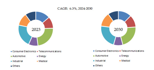
According to the new market research report “Global SMD Thick Film Resistor Market Report 2023-2030”, published by QYResearch, the global SMD Thick Film Resistor market size is projected to reach USD 2.55 billion by 2030, at a CAGR of 6.3% during the forecast period.
Figure. Global SMD Thick Film Resistor Market Size (US$ Million), 2019-2030

Above data is based on report from QYResearch: Global SMD Thick Film Resistor Market Report 2023-2030 (published in 2024). If you need the latest data, plaese contact QYResearch.
Figure. Global SMD Thick Film Resistor Top 14 Players Ranking and Market Share (Ranking is based on the revenue of 2023, continually updated)

Above data is based on report from QYResearch: Global SMD Thick Film Resistor Market Report 2023-2030 (published in 2024). If you need the latest data, plaese contact QYResearch.
According to QYResearch Top Players Research Center, the global key manufacturers of SMD Thick Film Resistor include Yageo, KOA, Walsin Technology, Vishay, Fenghua Advanced Technology, Ta-I Technology, Panasonic, Samsung Electro-Mechanics, Rohm, UniOhm, etc. In 2023, the global top 10 players had a share approximately 84.0% in terms of revenue.
Figure. SMD Thick Film Resistor, Global Market Size, Split by Product Segment
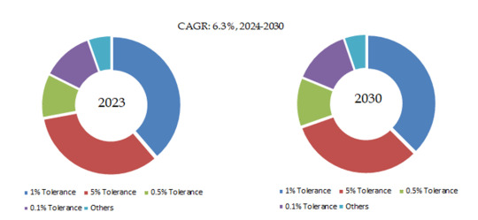
Based on or includes research from QYResearch: Global SMD Thick Film Resistor Market Report 2023-2030.
In terms of product type, 1% Tolerance is the largest segment, hold a share of 38.7%,
Figure. SMD Thick Film Resistor, Global Market Size, Split by Application Segment
Based on or includes research from QYResearch: Global SMD Thick Film Resistor Market Report 2023-2030.
In terms of product application, Automotive is the largest application, hold a share of 23.4%,
Figure. SMD Thick Film Resistor, Global Market Size, Split by Region
Based on or includes research from QYResearch: Global SMD Thick Film Resistor Market Report 2023-2030.
Market Drivers:
D1: Consumer Electronics Boom: The continuous growth in consumer electronics, including smart devices, home appliances, and entertainment systems, has contributed to the demand for SMD Thick Film Resistors in various applications.
D2: There is a stable demand for SMD thick film resistors in the automotive, industrial, medical, Telecommunication, energy and other fields of various countries.
D3: Growth in Demand in Emerging Economies such as China, India, Southeast Asia, Brazil etc.
Restraint:
R1: Price Volatility: Fluctuations in raw material prices used in SMD Thick Film Resistors, can affect production costs and subsequently impact pricing strategies.
R2: The design and R&D of SMD Thick Film Resistors require high-tech talents, and enterprises are facing the risk of brain drain.
R3: Global Economic Conditions: Economic downturns or uncertain market conditions can lead to reduced consumer spending on electronic devices, impacting the demand for SMD Thick Film Resistors.
Challenges:
C1: Miniaturization Demands: As technology advances, there's a constant need for smaller and more compact electronic devices. This requires SMD Thick Film Resistors to be even smaller while maintaining or improving performance, posing a challenge in manufacturing and precision.
C2: Cost Pressure: The market often experiences price pressure due to competitive forces and cost-cutting demands from manufacturers. Balancing quality and cost-effectiveness become crucial to sustain profitability.
C3: Technological Advancements: Rapid advancements in technology lead to newer materials, manufacturing processes, and innovative designs. Keeping up with these advancements requires substantial investments in research and development to stay competitive.
About the Authors
Wei Qin
Lead Author
Semiconductor and Electronics
Email: [email protected]
About QYResearch
QYResearch founded in California, USA in 2007. It is a leading global market research and consulting company. With over 16 years’ experience and professional research team in various cities over the world QY Research focuses on management consulting, database and seminar services, IPO consulting, industry chain research and customized research to help our clients in providing non-linear revenue model and make them successful. We are globally recognized for our expansive portfolio of services, good corporate citizenship, and our strong commitment to sustainability. Up to now, we have cooperated with more than 60,000 clients across five continents. Let’s work closely with you and build a bold and better future.
QYResearch is a world-renowned large-scale consulting company. The industry covers various high-tech industry chain market segments, spanning the semiconductor industry chain (semiconductor equipment and parts, semiconductor materials, ICs, Foundry, packaging and testing, discrete devices, sensors, optoelectronic devices), photovoltaic industry chain (equipment, cells, modules, auxiliary material brackets, inverters, power station terminals), new energy automobile industry chain (batteries and materials, auto parts, batteries, motors, electronic control, automotive semiconductors, etc.), communication industry chain (communication system equipment, terminal equipment, electronic components, RF front-end, optical modules, 4G/5G/6G, broadband, IoT, digital economy, AI), advanced materials industry Chain (metal materials, polymer materials, ceramic materials, nano materials, etc.), machinery manufacturing industry chain (CNC machine tools, construction machinery, electrical machinery, 3C automation, industrial robots, lasers, industrial control, drones), food, beverages and pharmaceuticals, medical equipment, agriculture, etc.
0 notes
Text
PCB Manufacturing: From Hand Assembly to Automated Processes
Printed Circuit Boards (PCBs) are the backbone of modern electronics, enabling the functionality of devices we use daily. The journey of PCB manufacturing has seen a remarkable evolution from manual hand assembly to highly automated processes, revolutionizing the electronics industry. In this article, we explore this evolution, highlighting key milestones, technologies, and the impact on product quality and efficiency.
Manual Assembly Era
In the early days of electronics, PCBs were assembled manually, often involving tedious and labor-intensive processes. Components were soldered onto the board by skilled technicians, requiring precision and expertise. This era was characterized by limited production capacities, longer lead times, and higher chances of human error affecting product quality.
Introduction of Automated Assembly
The shift towards automated assembly processes marked a significant turning point in PCB manufacturing. Automated equipment such as pick-and-place machines, soldering robots, and inspection systems were introduced to streamline production, increase throughput, and enhance consistency. This automation reduced labor costs, improved efficiency, and enabled manufacturers to meet growing demands for electronic components.
Advancements in Surface Mount Technology (SMT)
Surface Mount Technology revolutionized PCB assembly by replacing through-hole components with smaller, lighter, and more densely packed surface-mount components. SMT components are placed directly onto the board's surface, eliminating the need for drilling holes and simplifying assembly processes. This technology paved the way for miniaturization, higher component densities, and improved electrical performance in electronic devices.
Integration of AI and Robotics
The integration of Artificial Intelligence (AI) and robotics further accelerated the evolution of PCB manufacturing. AI algorithms optimize production workflows, detect defects, and enhance quality control measures. Robotics automate repetitive tasks with precision and speed, reducing cycle times and improving overall production efficiency. These advancements empower manufacturers to achieve higher yields, lower defect rates, and consistent product quality.
Industry 4.0 and Smart Manufacturing
The emergence of Industry 4.0 and smart manufacturing concepts has brought PCB manufacturing to new heights of efficiency and connectivity. IoT (Internet of Things) devices, data analytics, and real-time monitoring systems enable predictive maintenance, remote diagnostics, and agile production planning. Smart factories leverage interconnected technologies to create flexible, responsive, and data-driven manufacturing environments, driving continuous improvement and innovation in PCB production.
Impact on Product Quality and Efficiency
The evolution of PCB manufacturing from hand assembly to automated processes has had a profound impact on product quality, efficiency, and market competitiveness. Benefits include:
Improved Quality Control: Automated inspection systems detect defects with greater accuracy, ensuring higher product reliability and customer satisfaction.
Enhanced Efficiency: Automated processes reduce production cycle times, increase throughput, and optimize resource utilization, leading to cost savings and faster time-to-market.
Miniaturization and Innovation: Advanced technologies enable smaller form factors, higher component densities, and innovative designs, fueling advancements in electronic products and applications.
Scalability and Flexibility: Automated manufacturing facilities can scale production volumes quickly and adapt to changing market demands, providing agility and competitive advantage.
Conclusion
The evolution of PCB manufacturing from manual hand assembly to automated processes represents a journey of innovation, efficiency, and continuous improvement. Technologies such as AI, robotics, SMT, and smart manufacturing have transformed the electronics industry, empowering manufacturers to deliver high-quality, reliable, and innovative PCB solutions to meet the demands of today's interconnected world. As we embrace the era of Industry 4.0, the future of PCB manufacturing promises even greater advancements in quality, efficiency, and technological sophistication.
0 notes
Last Seen Blogs

karlieaphrodite
welcome to your friendly neighborhood titty deale

mais-nerdy-corner
✨Author Mai✨
mais-nerdy-corner
✨Author Mai✨

cocowhtb
Sin título

holografrick
i draw