#processing semiconductor
Explore tagged Tumblr posts
Visit Tumblr Blog
Explore Tumblr blogs with no restrictions, modern design and the best experience.
Last Seen Tumblr Blogs


Fun Fact
Tumblr was named as a finalist in Lead411’s New York City Hot 125 in Aug 2010.
Text

Hydrogen annealing approach sets new efficiency record for kesterite solar cells
Photovoltaics (PVs), devices that can convert sunlight into electrical power, are becoming increasingly widespread and more people worldwide are now relying on them to generate electricity. Renewable energy engineers worldwide are working to identify materials and processes that could help to further reduce the costs of solar technologies, while further boosting their power-conversion-efficiencies (PCEs). A promising material for the development of PVs is wide-bandgap kesterite Cu2ZnSnS4 (CZTS), a semiconductor that exhibits a large energy gap and could thus absorb light more efficiently. In contrast with silicon, which is currently the primary material used to fabricate PV technology, CZTS is non-toxic and made of elements that are abundant on Earth. Thus, it could be used to create more sustainable and affordable solar cells.
Read more.
#Materials Science#Science#Hydrogen#Materials processing#Solar power#Efficiency#Photovoltaics#Kesterite#Semiconductors#University of New South Wales
24 notes
·
View notes
Text
email SENT! let's see if i get this job 😹
#i rly want it bro it's literally what i want to do w my life#like#semiconductor processing is so interesting#i must get this job and gain experience or i might cry#ashlee's bs
3 notes
·
View notes
Text
Explore Texas Instruments Incorporated stock forecast for 2025–2029, with price targets, dividend insights, and investment tips. #TexasInstrumentsIncorporated #TXN #TXNstockforecast #Semiconductorstocks #Dividendstocks #Stockpriceprediction #Investmentopportunities #
#2025 stock picks#Analog and embedded processing market trends#Analog chips#Best dividend stocks for 2025#Dividend Stocks#Embedded processing#How to invest in Texas Instruments stock#Investment#Investment Insights#Investment Opportunities#Is Texas Instruments a good investment in 2025?#Semiconductor industry outlook for Texas Instruments#Semiconductor stocks#Stock Forecast#Stock Insights#Stock price prediction#Texas Instruments Incorporated#Texas Instruments stock#Texas Instruments stock analysis and price targets#Texas Instruments stock buy recommendation#Texas Instruments stock price forecast 2025–2029#TI stock analysis#TXN#TXN stock dividend yield and buyback policy#TXN stock forecast#TXN stock performance and competitive landscape
1 note
·
View note
Text
to add even more fuel to the “Electra as a Musk figure pisses me off beyond belief” fire, god rail as an industry is the antithesis of everything he stands for. It’s all so regulated and clunky and high reliability/durability is a huge thing in it, it’s literally where stuff like metal fatigue as a serious topic came from. It’s anything but “move fast and break things” and on the ground tends to be hostile to tech changing, ESPECIALLY if unproven. It has way more in common with the high-reliability circuit board factory I worked at that still used a shocking amount of 80s equipment because changing methods and equipment was such a slow process.
#even semiconductor manufacturing uses a surprising amount of old equipment for processes that don’t need stuff more advanced#lol half my current job is retrofitting that older stuff
1 note
·
View note
Text
0 notes
Text
#GPU Market#Graphics Processing Unit#GPU Industry Trends#Market Research Report#GPU Market Growth#Semiconductor Industry#Gaming GPUs#AI and Machine Learning GPUs#Data Center GPUs#High-Performance Computing#GPU Market Analysis#Market Size and Forecast#GPU Manufacturers#Cloud Computing GPUs#GPU Demand Drivers#Technological Advancements in GPUs#GPU Applications#Competitive Landscape#Consumer Electronics GPUs#Emerging Markets for GPUs
0 notes
Text
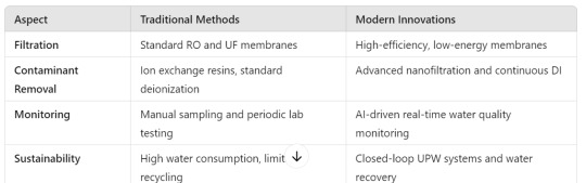
Ultrapure Water Production: Advanced Technologies and Challenges in Semiconductor Fabrication
Semiconductor fabrication demands an exceptionally high level of water purity to ensure defect-free chip production. Ultrapure water (UPW) is used throughout the manufacturing process for wafer cleaning, etching, and rinsing, requiring the removal of even the smallest impurities at the molecular level. Achieving this level of purity involves advanced water treatment processes that eliminate dissolved solids, organic compounds, and microscopic particulates. This article provides a step-by-step breakdown of UPW production, explores the challenges of maintaining extreme purity, and discusses the latest innovations in real-time monitoring, nanofiltration, and sustainable water management.
Step-by-Step Process of Ultrapure Water Production
Producing ultrapure water for semiconductor manufacturing requires a multi-stage treatment system designed to remove all contaminants, including dissolved ions, bacteria, organic molecules, and nanoparticles.
Pre-Treatment: Raw water undergoes filtration and chemical conditioning to remove large particles, suspended solids, and microbial contaminants.
Reverse Osmosis (RO): A semi-permeable membrane removes up to 99% of dissolved salts, bacteria, and organic compounds, forming the foundation of UPW production.
Deionization (DI): Ion exchange resins eliminate remaining dissolved ions, ensuring extremely low conductivity in the water.
Ultrafiltration (UF): A fine membrane filtration system removes microscopic particles and endotoxins that could compromise wafer processing.
UV Oxidation: High-intensity ultraviolet light is used to break down organic contaminants and disinfect the water by destroying bacteria and viruses.
Degasification: Dissolved gases such as oxygen and carbon dioxide are removed to prevent oxidation and unwanted chemical reactions in semiconductor fabrication.
Final Polishing: A combination of microfiltration and high-efficiency ion exchange further refines the water, ensuring it meets the highest purity standards required for semiconductor manufacturing.
Challenges in UPW Production for Semiconductor Fabs
Despite the effectiveness of these treatment processes, several challenges must be addressed to maintain UPW purity and ensure system efficiency:
Maintaining Extreme Purity Levels: Any deviation in water quality can result in contamination, leading to defects in semiconductor wafers. Real-time monitoring and precise control of UPW systems are essential.
System Reliability and Operational Efficiency: Downtime in UPW systems can halt semiconductor production, requiring highly efficient, redundant purification processes.
Water Wastage and Sustainability: UPW production consumes significant amounts of water, making waste reduction and recycling crucial for both cost-efficiency and environmental responsibility.
Microbial and Particulate Contamination: Even ultra-low levels of bacteria or nanoparticles can interfere with semiconductor fabrication, necessitating advanced filtration and disinfection techniques.
Innovations in UPW Production Technologies
To address these challenges, new technologies are continuously being developed to improve ultrapure water treatment.
Real-Time Monitoring and Smart Sensors: AI-powered monitoring systems detect impurities instantly, allowing for automated adjustments to maintain water quality.
Nanofiltration for Enhanced Purity: This advanced membrane technology provides an additional layer of purification, removing even the smallest contaminants without excessive energy consumption.
Energy-Efficient UPW Systems: New-generation RO and UF membranes require lower pressure, reducing energy use while maintaining superior filtration efficiency.
Sustainable Water Recycling Technologies: Semiconductor manufacturers are investing in water recovery and reuse strategies to minimize waste and optimize resource utilization.
Traditional vs. Modern UPW Treatment Methods
Comparing conventional water purification techniques with modern innovations highlights the evolution of UPW
Conclusion
Ultrapure water is a critical component in semiconductor fabrication, requiring precise treatment processes and cutting-edge purification technologies. The continuous evolution of UPW production, driven by real-time monitoring, nanofiltration, and sustainable water management, ensures that semiconductor fabs achieve higher efficiency while minimizing contamination risks. As the demand for advanced semiconductors grows, innovative ultrapure water systems will remain essential in maintaining high production standards and environmental sustainability.
SWJAL PROCESS Pvt. Ltd. offers industry-leading ultra pure water solutions tailored for semiconductor manufacturing, ensuring unmatched purity and reliability in every process.
#high purity water plant#high purity water system#high pure water for semiconductor productionr#pure water solution for critical industry#Swjal process
0 notes
Text
SiC Seeding for Sustainable Green Energy: An Overview of SiC Crystal Growth and Wafer Processing
Silicon carbide (SiC) is rapidly emerging as a game-changing material in the semiconductor industry. Its superior performance in high-power applications — such as electric vehicles, power grids, and renewable energy — sets it apart from traditional silicon-based solutions. With a wide bandgap, high electron mobility, and excellent thermal conductivity, SiC enables more efficient power devices, reducing energy loss and enhancing performance.
This article explores SiC crystal growth and wafer processing techniques, shedding light on the challenges and innovations driving the scalability and cost-effectiveness of SiC semiconductor manufacturing.
1. Fundamentals of SiC Crystal Growth and Material Properties
1.1 SiC Requirements
SiC is integral to modern power applications due to its exceptional properties, including a bandgap three times wider than silicon and a significantly higher critical electric field. These characteristics enable SiC-based power devices to operate at higher voltages and temperatures while reducing power losses and heat dissipation requirements.
Orbit & Skyline Semiconductor Fab Services specializes in precision processing and advanced fabrication solutions tailored for SiC technology, ensuring high-performance outcomes for semiconductor manufacturers.
1.2 SiC Crystal Structure
Silicon carbide exists in over 250 polytypes, each with unique electrical properties. Among them, 4H-SiC is the most favored due to its high electron mobility, breakdown voltage, and thermal conductivity. However, growing SiC crystals at industrial scales presents significant challenges, primarily due to the high processing temperatures (exceeding 2000°C) and the slow growth rates required to maintain quality and minimize defects.
1.3 SiC Boule Growth Methods
The semiconductor industry primarily employs three major methods for growing SiC boules, with the Physical Vapor Transport (PVT) method being the most prevalent. PVT relies on sublimation due to the lack of a stable liquid phase for SiC. Despite its advantages, challenges such as micropipes, stacking faults, and dislocation densities persist.
Orbit & Skyline’s process engineering team optimizes growth techniques to maximize yield and reduce defects, ensuring superior wafer quality. By fine-tuning parameters such as temperature control and pressure regulation, we enhance SiC crystal production efficiency.
1.4 Physical Vapor Transport (PVT) Process
The PVT process involves melting high purity SiC powder in a growth chamber at temperatures exceeding 2000°C. The sublimated vapor then deposits onto a seed crystal, gradually forming a high-quality SiC boule. This method enables precise control over doping levels, essential for tailoring electrical characteristics. N-type doping (typically using nitrogen) enhances conductivity, while p-type doping (using aluminium) influences the polytype formation, affecting overall device performance.
2. From Boule to Epi-Ready Wafer
2.1 SiC Hardness and Processing Challenges
SiC is one of the hardest materials known, ranking 9–9.5 on the Mohs scale. This extreme hardness complicates the slicing and processing of SiC boules into wafers. Specialized grinding, lapping, and polishing techniques are required to achieve the precise dimensions necessary for semiconductor applications.
Orbit & Skyline’s Equipment Engineering services provide tailored solutions to overcome these challenges, ensuring precise wafer preparation for further processing.
2.2 Wafer Slicing and Surface Preparation
SiC boules undergo slicing using multi-wire saws coated with diamond slurry. This process must balance kerf loss (material waste) and throughput efficiency. Following slicing, wafers undergo lapping to ensure uniform thickness and surface quality, crucial for subsequent epitaxial growth.
2.3 Epi-Ready Polishing and Surface Finishing
To achieve EPI-ready surfaces, wafers undergo Chemical Mechanical Polishing (CMP), combining mechanical abrasion with chemical etching. Innovations in CMP technology, such as rapid thinning techniques, enhance material removal rates while maintaining surface integrity. This ensures defect-free epitaxial layers, which are critical for high-performance semiconductor applications.
3. Epitaxial Growth and Doping of SiC
3.1 High-Temperature Chemical Vapor Deposition (HT-CVD)
Epitaxial growth involves depositing thin, defect-free SiC layers on wafers to enhance electrical performance. HT-CVD is the industry standard, offering precise control over doping concentration and layer thickness. By using silicon and carbon precursors, diluted in hydrogen or argon carrier gases, HT-CVD facilitates uniform SiC layer growth.
3.2 Alternative Epitaxy Methods
Other epitaxy methods, such as Molecular Beam Epitaxy (MBE) and Liquid Phase Epitaxy (LPE), have been explored. However, challenges in impurity control, growth rate limitations, and scalability make HT-CVD the preferred approach for large-scale SiC production.
3.3 Scaling to 8” and 200mm Wafers
With the industry shifting towards 8” (200mm) SiC wafers, significant improvements in slicing and polishing processes have been made. Advanced wafer thinning and surface finishing techniques ensure high yield and minimal defect rates. The transition to larger wafers increases device yield per wafer while optimizing fabrication costs.
Conclusion
SiC wafer technology continues to evolve, with advances in boule growth, wafer slicing, and epitaxial deposition driving the transition from 6” to 8” wafers. The industry’s focus on improving material quality and reducing processing costs ensures that SiC remains a competitive alternative to silicon in high-power applications.
Orbit & Skyline brings 15+ years of expertise, and a global team of 500+ engineers dedicated to advancing semiconductor technologies. As a trusted partner in the industry, we provide innovative solutions for SiC processing, fabrication, and equipment engineering.
For partnership inquiries, reach out to us at [email protected]
#semiconductor#Top Semiconductor Companies in India#Semiconductor Companies#Semiconductor Fab#Process Engineer
1 note
·
View note
Text
詠翊科技有限公司
YONG YI CNCTETCH.Co.,LTD.
詠翊科技創立於2005年4月,團隊已擁有CNC銑床加工約二十年之專業加工經驗,其生產領域涵蓋電子、光學及半導體自動化設備…等產業。
目前廠內設備共有CNC銑床機台10台、傳統銑床7台、傳統車床及平面研磨機台共近20台精密設備。 此外亦陸續積極擴大規模及採購新的生產設備以有效擴張產能及服務範圍。 本公司可依據客戶之需求協助開發設計加工,各零件接單生產流程皆採嚴謹加工生產技術及品管檢驗作業,搭配各項表面處理,如:陽極、電鍍、代工代料代表處,全都處理到好。
詠翊科技本著「感恩的心、勤儉向上、追求創新、技術增長,並懷著努力不懈的敬業態度」,贏得各設備大廠及日本客戶一致的好評與信任。日後亦會秉持我們一貫的優良作風,「品質第一、快速交貨」,繼續為客戶服務。
Yongyi Technology was founded in April 2005. The team has about 20 years of professional processing experience in CNC milling machine processing. Its production fields cover electronics, optics and semiconductor automation equipment… and other industries.
Currently, the factory has 10 CNC milling machines, 7 traditional milling machines, and nearly 20 traditional lathes and surface grinding machines, a total of nearly 20 precision equipment. In addition, it has also been actively expanding its scale and purchasing new production equipment to effectively expand its production capacity and service scope. Our company can assist in the development, design and processing according to the needs of customers. The production process of each part order adopts rigorous processing and production technology and quality control inspection operations, with various surface treatments, such as anodizing, electroplating, and OEM representative offices. Handled well.
Yongyi Technology has won unanimous praise and trust from major equipment manufacturers and Japanese customers with its “gratitude, thrift, pursuit of innovation, technological growth, and unremitting dedication”. In the future, we will uphold our consistent good style of “quality first, fast delivery” and continue to serve customers.

#cncprocessing#cncprecision processing#semiconductor components#automation equipment#precision components#robot arm#stainless steel processing#engineering plastic#ceramic processing#cnc加工#cnc精密加工#半導體零組件#自動化設備#精密零組件#機器手臂#不鏽鋼加工#工程塑膠#陶瓷加工
0 notes
Text
University of Missouri scientists are unlocking the secrets of halide perovskites -- a material that's poised to reshape our future by bringing us closer to a new age of energy-efficient optoelectronics. Suchi Guha and Gavin King, two physics professors in Mizzou's College of Arts and Science, are studying the material at the nanoscale: a place where objects are invisible to the naked eye. At this level, the extraordinary properties of halide perovskites come to life, thanks to the material's unique structure of ultra-thin crystals -- making it astonishingly efficient at converting sunlight into energy. Think solar panels that are not only more affordable but also far more effective at powering homes. Or LED lights that burn brighter and last longer while consuming less energy.
Read more.
#Materials Science#Science#Perovskites#Halide perovskites#Halogens#University of Missouri#Layered materials#Crystals#Semiconductors#Thin films#Materials processing
22 notes
·
View notes
Text
Machine learning applications in semiconductor manufacturing
Machine Learning Applications in Semiconductor Manufacturing: Revolutionizing the Industry
The semiconductor industry is the backbone of modern technology, powering everything from smartphones and computers to autonomous vehicles and IoT devices. As the demand for faster, smaller, and more efficient chips grows, semiconductor manufacturers face increasing challenges in maintaining precision, reducing costs, and improving yields. Enter machine learning (ML)—a transformative technology that is revolutionizing semiconductor manufacturing. By leveraging ML, manufacturers can optimize processes, enhance quality control, and accelerate innovation. In this blog post, we’ll explore the key applications of machine learning in semiconductor manufacturing and how it is shaping the future of the industry.
Predictive Maintenance
Semiconductor manufacturing involves highly complex and expensive equipment, such as lithography machines and etchers. Unplanned downtime due to equipment failure can cost millions of dollars and disrupt production schedules. Machine learning enables predictive maintenance by analyzing sensor data from equipment to predict potential failures before they occur.
How It Works: ML algorithms process real-time data from sensors, such as temperature, vibration, and pressure, to identify patterns indicative of wear and tear. By predicting when a component is likely to fail, manufacturers can schedule maintenance proactively, minimizing downtime.
Impact: Predictive maintenance reduces equipment downtime, extends the lifespan of machinery, and lowers maintenance costs.
Defect Detection and Quality Control
Defects in semiconductor wafers can lead to significant yield losses. Traditional defect detection methods rely on manual inspection or rule-based systems, which are time-consuming and prone to errors. Machine learning, particularly computer vision, is transforming defect detection by automating and enhancing the process.
How It Works: ML models are trained on vast datasets of wafer images to identify defects such as scratches, particles, and pattern irregularities. Deep learning algorithms, such as convolutional neural networks (CNNs), excel at detecting even the smallest defects with high accuracy.
Impact: Automated defect detection improves yield rates, reduces waste, and ensures consistent product quality.
Process Optimization
Semiconductor manufacturing involves hundreds of intricate steps, each requiring precise control of parameters such as temperature, pressure, and chemical concentrations. Machine learning optimizes these processes by identifying the optimal settings for maximum efficiency and yield.
How It Works: ML algorithms analyze historical process data to identify correlations between input parameters and output quality. Techniques like reinforcement learning can dynamically adjust process parameters in real-time to achieve the desired outcomes.
Impact: Process optimization reduces material waste, improves yield, and enhances overall production efficiency.
Yield Prediction and Improvement
Yield—the percentage of functional chips produced from a wafer—is a critical metric in semiconductor manufacturing. Low yields can result from various factors, including process variations, equipment malfunctions, and environmental conditions. Machine learning helps predict and improve yields by analyzing complex datasets.
How It Works: ML models analyze data from multiple sources, including process parameters, equipment performance, and environmental conditions, to predict yield outcomes. By identifying the root causes of yield loss, manufacturers can implement targeted improvements.
Impact: Yield prediction enables proactive interventions, leading to higher productivity and profitability.
Supply Chain Optimization
The semiconductor supply chain is highly complex, involving multiple suppliers, manufacturers, and distributors. Delays or disruptions in the supply chain can have a cascading effect on production schedules. Machine learning optimizes supply chain operations by forecasting demand, managing inventory, and identifying potential bottlenecks.
How It Works: ML algorithms analyze historical sales data, market trends, and external factors (e.g., geopolitical events) to predict demand and optimize inventory levels. Predictive analytics also helps identify risks and mitigate disruptions.
Impact: Supply chain optimization reduces costs, minimizes delays, and ensures timely delivery of materials.
Advanced Process Control (APC)
Advanced Process Control (APC) is critical for maintaining consistency and precision in semiconductor manufacturing. Machine learning enhances APC by enabling real-time monitoring and control of manufacturing processes.
How It Works: ML models analyze real-time data from sensors and equipment to detect deviations from desired process parameters. They can automatically adjust settings to maintain optimal conditions, ensuring consistent product quality.
Impact: APC improves process stability, reduces variability, and enhances overall product quality.
Design Optimization
The design of semiconductor devices is becoming increasingly complex as manufacturers strive to pack more functionality into smaller chips. Machine learning accelerates the design process by optimizing chip layouts and predicting performance outcomes.
How It Works: ML algorithms analyze design data to identify patterns and optimize layouts for performance, power efficiency, and manufacturability. Generative design techniques can even create novel chip architectures that meet specific requirements.
Impact: Design optimization reduces time-to-market, lowers development costs, and enables the creation of more advanced chips.
Fault Diagnosis and Root Cause Analysis
When defects or failures occur, identifying the root cause can be challenging due to the complexity of semiconductor manufacturing processes. Machine learning simplifies fault diagnosis by analyzing vast amounts of data to pinpoint the source of problems.
How It Works: ML models analyze data from multiple stages of the manufacturing process to identify correlations between process parameters and defects. Techniques like decision trees and clustering help isolate the root cause of issues.
Impact: Faster fault diagnosis reduces downtime, improves yield, and enhances process reliability.
Energy Efficiency and Sustainability
Semiconductor manufacturing is energy-intensive, with significant environmental impacts. Machine learning helps reduce energy consumption and improve sustainability by optimizing resource usage.
How It Works: ML algorithms analyze energy consumption data to identify inefficiencies and recommend energy-saving measures. For example, they can optimize the operation of HVAC systems and reduce idle time for equipment.
Impact: Energy optimization lowers operational costs and reduces the environmental footprint of semiconductor manufacturing.
Accelerating Research and Development
The semiconductor industry is driven by continuous innovation, with new materials, processes, and technologies being developed regularly. Machine learning accelerates R&D by analyzing experimental data and predicting outcomes.
How It Works: ML models analyze data from experiments to identify promising materials, processes, or designs. They can also simulate the performance of new technologies, reducing the need for physical prototypes.
Impact: Faster R&D cycles enable manufacturers to bring cutting-edge technologies to market more quickly.
Challenges and Future Directions
While machine learning offers immense potential for semiconductor manufacturing, there are challenges to overcome. These include the need for high-quality data, the complexity of integrating ML into existing workflows, and the shortage of skilled professionals. However, as ML technologies continue to evolve, these challenges are being addressed through advancements in data collection, model interpretability, and workforce training.
Looking ahead, the integration of machine learning with other emerging technologies, such as the Internet of Things (IoT) and digital twins, will further enhance its impact on semiconductor manufacturing. By embracing ML, manufacturers can stay competitive in an increasingly demanding and fast-paced industry.
Conclusion
Machine learning is transforming semiconductor manufacturing by enabling predictive maintenance, defect detection, process optimization, and more. As the industry continues to evolve, ML will play an increasingly critical role in driving innovation, improving efficiency, and ensuring sustainability. By harnessing the power of machine learning, semiconductor manufacturers can overcome challenges, reduce costs, and deliver cutting-edge technologies that power the future.
This blog post provides a comprehensive overview of machine learning applications in semiconductor manufacturing. Let me know if you’d like to expand on any specific section or add more details!
#semiconductor manufacturing#Machine learning in semiconductor manufacturing#AI in semiconductor industry#Predictive maintenance in chip manufacturing#Defect detection in semiconductor wafers#Semiconductor process optimization#Yield prediction in semiconductor manufacturing#Advanced Process Control (APC) in semiconductors#Semiconductor supply chain optimization#Fault diagnosis in chip manufacturing#Energy efficiency in semiconductor production#Deep learning for semiconductor defects#Computer vision in wafer inspection#Reinforcement learning in semiconductor processes#Semiconductor yield improvement using AI#Smart manufacturing in semiconductors#AI-driven semiconductor design#Root cause analysis in chip manufacturing#Sustainable semiconductor manufacturing#IoT in semiconductor production#Digital twins in semiconductor manufacturing
0 notes
Text
From Silicon To Chips: Understanding The Semiconductor Manufacturing Process
Semiconductors are at the core of modern technology, powering everything from smartphones to supercomputers. The process of manufacturing semiconductors is highly complex, involving multiple stages of precision engineering and advanced materials science. This blog explores the key steps involved in transforming raw silicon into functional semiconductor chips.
1. Silicon Extraction and Purification
The semiconductor production process begins with silicon, which is derived from silica (SiO₂), commonly found in sand. To be used in semiconductor manufacturing, silicon must be purified to an extremely high level—99.9999% or higher. This is achieved through a process called the Czochralski method, in which raw silicon is melted and crystallized into a large, highly pure monocrystalline silicon ingot.
2. Wafer Formation
The purified silicon ingot is sliced into thin discs known as wafers using a diamond-tipped saw. These wafers, typically 200mm to 300mm in diameter, undergo chemical and mechanical polishing to achieve a smooth, defect-free surface. The quality of the wafer surface is crucial, as any imperfections can affect the performance of the final semiconductor chip.
3. Photolithography and Patterning
One of the most critical steps in semiconductor manufacturing is photolithography, which is used to create intricate circuit patterns on the wafer. The process involves several key steps:
Coating: The wafer is covered with a light-sensitive material called photoresist.
Exposure: A mask containing the circuit design is placed over the wafer, and UV light is projected through it. The light alters the chemical properties of the exposed photoresist.
Etching: The unwanted photoresist is removed, leaving behind the circuit pattern on the wafer.
This process is repeated multiple times, with each layer forming a different part of the semiconductor’s structure.
4. Doping and Ion Implantation
To modify the electrical properties of silicon, impurities are introduced through a process called doping. Ion implantation is commonly used to precisely insert atoms such as phosphorus or boron into specific regions of the silicon wafer, altering its conductivity and enabling transistor functionality.
5. Deposition and Layering
Semiconductor chips consist of multiple layers of materials, including metals and insulators. These layers are deposited onto the wafer using techniques like:
Chemical Vapor Deposition (CVD) – Uses chemical reactions to form thin films on the wafer.
Physical Vapor Deposition (PVD) – Deposits materials via high-energy plasma.
Each layer plays a role in forming transistors, capacitors, and interconnects essential for the chip’s operation.
6. Etching and Planarization
After deposition, unwanted material is removed using etching techniques. Wet etching (chemical-based) and dry etching (plasma-based) are used depending on the required precision. Chemical Mechanical Planarization (CMP) is then applied to smooth the wafer surface, ensuring uniformity across layers.
7. Testing and Packaging
Once fabrication is complete, the wafers undergo electrical testing to identify defective chips. Functional chips are then cut from the wafer and enclosed in protective packaging. The packaging process involves attaching the chip to a circuit board, adding wiring for connectivity, and sealing it to protect against environmental damage.
The semiconductor manufacturing process is a highly sophisticated and precise operation, requiring advanced materials, equipment, and engineering techniques. As technology continues to evolve, manufacturers are constantly pushing the boundaries of miniaturization and efficiency, enabling the development of smaller, faster, and more powerful semiconductor chips.
0 notes
Text
Immersion Heaters for Semiconductor and screw plug immersion heaters

Process Technology manufactures and supplies various types of immersion heaters; screw plug immersion heaters and semiconductor heaters. These immersion heaters are specially intended for direct immersion heating of liquid, increase performance in the industrial application. Different chemical compatibility and different temperatures make sure Process Technology can provide you the right heat exchanger for your heating needs.
For more details Visit: https://www.processtechnology.com/products/electric-immersion-heaters/
#processtechnology#technology#immersionheaters#heaters#electric#process#thermalpower#Semiconductor#screwplugimmersionheaters#immersionheatersforwater
0 notes
Text
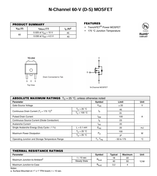
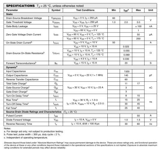
Application of VBE1638 MOSFET in Automotive Instrument Control Unit: Enhancing Power Management and Signal Processing
With the continuous advancement of automotive electronics technology, the Instrument Control Unit (ICU) serves as a crucial module in automotive electronic systems, responsible for processing and displaying key vehicle information. To meet the high demands for efficiency and reliability in modern vehicles, the ICU module requires superior performance in power management and switching control. The VBE1638 MOSFET, launched by VBsemi, provides an ideal solution with its excellent electrical characteristics, significantly improving the efficiency of signal processing and power management in ICU modules.

Efficient Power Management The ICU module must achieve stable power management under various load conditions, and the VBE1638, with its 60V drain-source voltage and maximum drain current of 45A, meets the demands of high-power applications. Utilizing advanced trench technology, it reduces on-resistance (with a typical value of only 25mΩ), which minimizes power loss, enhances power management efficiency, reduces heat generation, and extends the lifespan of the device.
Precise Signal Processing Precise signal processing is critical in automotive ICU modules, especially when dealing with complex sensor data. The VBE1638 MOSFET, with its low threshold voltage of 1.7V, enables quick response, ensuring the circuit can switch rapidly and adapt to different working states. Its +20V gate-source voltage (V<sub>GS</sub>) ensures high reliability and stability in various driving environments.
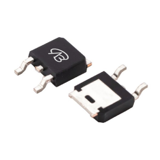
Robust Thermal Performance The automotive environment is highly demanding, requiring ICU modules to operate stably over long periods under high temperatures, vibrations, and current fluctuations. The VBE1638, packaged in a TO252 casing, offers excellent thermal performance, effectively preventing overheating in high-temperature environments, ensuring long-term stable operation, and reducing vehicle system maintenance costs.
Application Advantages The VBE1638 MOSFET is widely used in automotive instrument control unit modules, with optimized power management and power control performance ensuring reliable operation under varying load conditions. Whether in power management systems or complex control scenarios, the VBE1638 delivers stable and efficient performance.
Product Specifications
Model: VBE1638
Package: TO252
Polarity: N-channel
Drain-Source Voltage (VDS): 60V
Gate-Source Voltage (VGS): +20V
Threshold Voltage (Vth): 1.7V
On-Resistance (RDS(on) @VGS=4.5V): 30mΩ
On-Resistance (RDS(on) @VGS=10V): 25mΩ
Maximum Drain Current (ID): 45A
Technology: Trench
Other Applicable Areas
Power Tools: In the power tool sector, such as drills and hammers, MOSFETs provide stable power output. With its high current-handling capacity and low on-resistance, the VBE1638 is an ideal choice for these modules, ensuring high efficiency and stable performance under heavy workloads.
Industrial Automation: The VBE1638 is suitable for industrial automation equipment, including PLC controllers and motor drivers, supporting efficient automation and continuous innovation in smart manufacturing systems.
LED Lighting: In LED lighting applications, the VBE1638 is used in LED driver modules, providing stable and efficient power support, ensuring long life and low energy consumption for LED lamps, streetlights, and landscape lighting products.
As a high-performance MOSFET designed for automotive instrument control unit modules, the VBE1638 excels in power management and signal processing. Whether in complex signal processing scenarios or high-load power management, it helps enhance the overall efficiency and stability of ICU modules. As automotive electronics continue to evolve, the VBE1638 will play a vital role in more automotive applications, contributing to the innovation and upgrading of automotive electronic systems.
#MOSFETs,#Semiconductor,#Electronics,#Technology ,#Automotive,#Power management#On-resistance#Signal processing
0 notes
Text
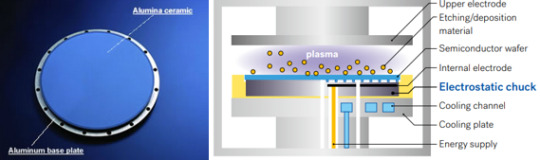
Global Top 14 Companies Accounted for 96% of total Electrostatic Chuck for Semiconductor Process market (QYResearch, 2021)
An electrostatic chuck is a component inside semiconductor equipment that is used to hold the semiconductor wafer. In the IoT Society, the demand for semiconductor is growing, which in turn has led to annual increases in the need for installing semiconductor-manufacturing equipment.
The Electrostatic Chuck for Semiconductor Process market covers Coulomb Type, Johnsen-Rahbek (JR) Type, etc. The typical players include Applied Materials, Lam Research, SHINKO, TOTO, Sumitomo Osaka Cement, Creative Technology Corporation, Kyocera, Entegris, etc.
According to the new market research report “Global Electrostatic Chuck for Semiconductor Process Market Report 2023-2029”, published by QYResearch, the global Electrostatic Chuck for Semiconductor Process market size is projected to reach USD 2.55 billion by 2029, at a CAGR of 5.3% during the forecast period.
Figure. Global Electrostatic Chuck for Semiconductor Process Market Size (US$ Million), 2018-2029

Figure. Global Electrostatic Chuck for Semiconductor Process Top 14 Players Ranking and Market Share (Ranking is based on the revenue of 2022, continually updated)

The global key manufacturers of Electrostatic Chuck for Semiconductor Process include Applied Materials, Lam Research, SHINKO, TOTO, Sumitomo Osaka Cement, Creative Technology Corporation, Kyocera, Entegris, NTK CERATEC, II-VI M Cubed, etc. In 2021, the global top five players had a share approximately 93.0% in terms of revenue.
About QYResearch
QYResearch founded in California, USA in 2007.It is a leading global market research and consulting company. With over 16 years’ experience and professional research team in various cities over the world QY Research focuses on management consulting, database and seminar services, IPO consulting, industry chain research and customized research to help our clients in providing non-linear revenue model and make them successful. We are globally recognized for our expansive portfolio of services, good corporate citizenship, and our strong commitment to sustainability. Up to now, we have cooperated with more than 60,000 clients across five continents. Let’s work closely with you and build a bold and better future.
QYResearch is a world-renowned large-scale consulting company. The industry covers various high-tech industry chain market segments, spanning the semiconductor industry chain (semiconductor equipment and parts, semiconductor materials, ICs, Foundry, packaging and testing, discrete devices, sensors, optoelectronic devices), photovoltaic industry chain (equipment, cells, modules, auxiliary material brackets, inverters, power station terminals), new energy automobile industry chain (batteries and materials, auto parts, batteries, motors, electronic control, automotive semiconductors, etc.), communication industry chain (communication system equipment, terminal equipment, electronic components, RF front-end, optical modules, 4G/5G/6G, broadband, IoT, digital economy, AI), advanced materials industry Chain (metal materials, polymer materials, ceramic materials, nano materials, etc.), machinery manufacturing industry chain (CNC machine tools, construction machinery, electrical machinery, 3C automation, industrial robots, lasers, industrial control, drones), food, beverages and pharmaceuticals, medical equipment, agriculture, etc.
0 notes