#spintronics
Text
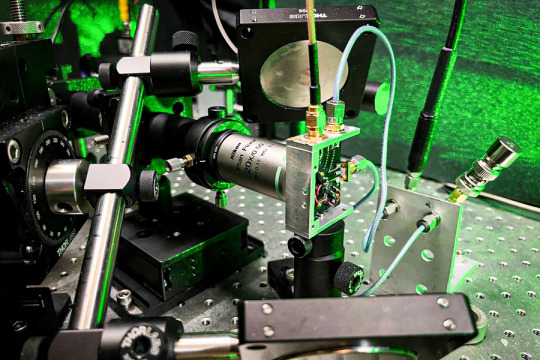
Scientists discover single atom defect in 2D material can hold quantum information at room temperature
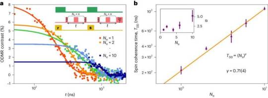
Scientists have discovered that a "single atomic defect" in a layered 2D material can hold onto quantum information for microseconds at room temperature, underscoring the potential of 2D materials in advancing quantum technologies.
The defect, found by researchers from the Universities of Manchester and Cambridge using a thin material called hexagonal boron nitride (hBN), demonstrates spin coherence—a property where an electronic spin can retain quantum information—under ambient conditions. They also found that these spins can be controlled with light.
Up until now, only a few solid-state materials have been able to do this, marking a significant step forward in quantum technologies.
The findings, published in Nature Materials, further confirm that the accessible spin coherence at room temperature is longer than the researchers initially imagined it could be.
Read more.
#Materials Science#Science#Defects#Quantum mechanics#2D materials#Layered materials#Boron nitride#Boron#Nitrides#Spintronics#University of Manchester
22 notes
·
View notes
Text
Study shows robotic third thumb enhances dexterity across diverse users, highlights need for inclusive design

- By Nuadox Crew -
Researchers at the University of Cambridge (UK) demonstrated that the Third Thumb, a robotic prosthetic, can be quickly mastered by a diverse range of people, enhancing manual dexterity.
Their study emphasizes the importance of inclusive design to ensure that new technologies benefit everyone, including marginalized communities.
The Third Thumb, controlled by foot pressure sensors, was tested on 596 participants aged 3 to 96, showing that nearly all could use it effectively within a minute.
Performance varied but showed no gender or handedness bias. The study underscores the need for early-stage inclusivity in developing wearable technologies to ensure accessibility and functionality for a wide range of users.
youtube
Video: "Testing the Third Thumb" by University of Cambridge, YouTube.
Read more at University of Cambridge
Header image credit: Dani Clode Design & The Plasticity Lab.
Scientific paper: Clode, D & Dowdall, L et al. Assessing First Time Usability of a Hand Augmentation Device in a Large Sample of Diverse Users. Science Robotics; 29 May 2024; DOI: 10.1126/scirobotics.adk5183
--
Other recent news:
Spintronics Advancements: Researchers have made a new milestone in spintronics, which could revolutionize electronics by better predicting and controlling spin currents, studying magnetic properties, and temperature effects on materials.
Tandem Solar Cells: Tandem solar cells have achieved over 20% efficiency, marking a significant step forward in solar technology.
NASA’s X-59 Quiet Supersonic Aircraft: NASA’s X-59 quiet supersonic aircraft project has passed a critical milestone, setting the stage for future flight tests.
Lithium Batteries: Korean researchers have developed a revolutionary new lightweight structure for lithium batteries, enhancing ion transport and battery performance.
“Metaholograms”: Scientists have developed a new type of hologram that could transform AR/VR technologies by enabling crosstalk-free, high-fidelity image projection with increased information capacity.
Memristors Mimic Neural Timekeeping: An AI chip breakthrough has occurred with memristors that can mimic the timekeeping of neurons.
#robotics#hand#spintronics#solar energy#energy#nasa#space#x59#lithium#batteries#vr#ar#metaholograms#memristors#ai#semiconductors
0 notes
Text


🐔 or 🥚❓


#filtration#air filter#big tech#technology#tech#spintronics#infrastructure#architecture#cityscape#industrial#development
1 note
·
View note
Text

𝐍𝐚𝐧𝐨𝐦𝐚𝐭𝐞𝐫𝐢𝐚𝐥𝐬: Nanoscience focuses on understanding the properties and behavior of nanomaterials, which can exhibit unique properties due to their small size and high surface area.
𝐈𝐧𝐭𝐞𝐫𝐝𝐢𝐬𝐜𝐢𝐩𝐥𝐢𝐧𝐚𝐫𝐲 𝐍𝐚𝐭𝐮𝐫𝐞: Nanoscience and nanotechnology draw from multiple disciplines, including physics, chemistry, biology, engineering, and materials science, to explore phenomena at the nanoscale.
Visit @ https://symbiosisonlinepublishing.com/nanoscience-technology/
#nanoscience#technology#nanosciencetech#nanostructures#nanometerscales#transmissionelectronmicroscopy#nanoscalematerials#nanomedicine#carbondots#nanofabrication#nanolithography#photonics#Macroscope#spintronics#nanomotor#insulintherapy#molecularmachine#nanodevices#journal#journals#pubmed#peerreview#peerreviewed#OpenAccess#openaccessjournal#symbiosisonlinepublishing
1 note
·
View note
Text


Had a great week at Diamond Light Source during my summer studentship.
#student#physics student#physics studyblr#physics#Diamond Light Source#Harwell#Syncatron#PEEM#XMLD#XMCD#Spintronics
1 note
·
View note
Text
I want to buy something but it's not available in my country :(
0 notes
Text
Spintronics Technology: Reshaping the Market Landscape
The spintronics market is projected to reach a value of US$ 687.1 million in 2023, with a forecasted compound annual growth rate (CAGR) of 7.3% leading to a market size of US$ 1,394.2 million by 2033.
The introduction of spintronics technology has revolutionized the storage and processing of massive data, leading to increased market share. Further, the demand for spintronics is driven by its applications in hard drives, digital electronics, sensors, and more.
Spintronics utilizes the spin of electrons rather than their charges, enabling energy-efficient chips and memory-storage devices. Magnetic RAM (MRAM) has emerged as a prominent spintronics technology, offering large storage space and potentially replacing conventional RAMs.
Accelerate Your Success: Unlock the Secrets of the Spintronics Market – Download the Sample Report @
https://www.futuremarketinsights.com/reports/sample/rep-gb-5912
Spintronics enables increased data storage and is considered a rising nanotechnology trend. The adoption of spintronics devices, driven by their superior performance and low power consumption, is predicted to expand the market, particularly in smart devices, IoT, and memory components.
Cost savings in manufacturing and continual research and initiatives are key drivers for market growth. However, challenges such as a lack of awareness among end users and an incomplete understanding of the technology, as well as the need for control over spin from a distance, may restrain the market.
Key Takeaways:
North America holds a 28.9% global share in the spintronics market, driven by its advanced technological infrastructure and strong investment in research and development.
Germany has emerged as a leading player, with government support and prominent companies involved in spintronics technologies.
India, with a CAGR of 10.4%, showcases potential for spintronics adoption, particularly in the automotive industry.
The United Kingdom exhibits a growth trajectory of 8.1% with its innovative startups, research institutions, and spintronic companies driving advancements.
Semiconductor-based spintronics holds a market share of 44.5%, benefiting from advancements in materials and device designs.
Hard disks and MRAMs account for a significant share of 29.8%, enabling high storage densities and improved energy efficiency.
Ask an Analyst @
https://www.futuremarketinsights.com/ask-the-analyst/rep-gb-5912
These trends highlight the global growth and applications of spintronics across various regions and categories.
Competitive Landscape
The spintronics market is distinguished by increasing product penetration, limited product differentiation, and intense rivalry. Also, innovation is critical to gaining a competitive advantage. In recent years, certain important market participants, such as Avalanche Technology and Crocus Technologies, have obtained investment to further their product innovation. As a result, competitive rivalry is intense.
Renesas Electronic Corporation announced the development of circuit technology for an integrated spin-transfer torque magnetoresistive random-access memory (STT-MRAM) test chip with read and write operations produced on a 22-nm process in June 2022.
February 20, 2022 – The spin transport properties of nanoscale graphene-based electrical devices have been enhanced by researchers at the University of Manchester. The National Graphene Institute researchers created an extraordinarily high-quality graphene channel in partnership with Japan and internationally supported students from Ecuador and Mexico, eliminating interference or electronic doping by standard 2D tunnel interactions.
In September 2022, Avalanche Technology announced the availability of new High-Reliability Persistent SRAM (P-SRAM) memory devices manufactured on the 22nm manufacturing technology of UMC. Using Avalanche’s newest Spin Transfer Torque Magnetoresistive RAM technology, the third-generation product platform outperforms previous non-volatile solutions in terms of density, durability, reliability, and power.
Segmentation Analysis of the Spintronics Market
By Device Type:
Semiconductor Based Spintronics
Metallic Based Spintronics
Alloy Based Spintronics
By Application:
Magnetic Sensors
Hard Disks and MRAMs
Electric Vehicles
Quantum Computing
Others
By Region:
North America
Latin America
Europe
East Asia
South Asia
Oceania
The Middle East & Africa
0 notes
Text
Ruby: What would you be doing if you weren’t a hunter?
Jaune: What? I’m alright with numbers. Maybe make machines think. I’m not like Dr. Polendina. He sorta does it all. Information theory.
Ruby: What do you mean?
Jaune: I understand the statistical forces behind machine learning programs but he’s on another level. He made Penny. He actually understands the mechanisms behind consciousness. He has three doctorates. I don’t get it at all.
Ruby: You could ask him. He might explain it to you.
Jaune: I’ve bothered him about physics questions and spintronics too much already.
Ruby: What are spintronics?
Jaune: You can make photons and electrons do math based on their spin and chirality. That’s probably how brains and Penny actually function. But I don’t understand the physics behind it. How do point particles spin? I just don’t understand.
35 notes
·
View notes
Text

'Miracle' filter turns store-bought LEDs into spintronic devices
Traditional electronics use semiconductors to transmit data through bursts of charged carriers (electrons or holes) to convey messages in "1s" and "0s." Spintronic devices can process an order of magnitude more information by assigning binary code to the orientation of electrons' magnetic poles, a property known as spin— an "up" spin is a 1, a "down" is a 0.
A major barrier to commercial spintronics is setting and maintaining the electron spin orientation. Most devices tune spin-orientation using ferromagnets and magnetic fields, a burdensome and unreliable process. Decades of research has shown that carriers lose their spin orientation moving from materials with high-conductivity to low-conductivity—for example, from metallic ferromagnets to undoped silicon and conjugated polymer materials that make up most modern semiconductors.
For the first time, scientists transformed existing optoelectronic devices into ones that can control electron spin at room temperature, without a ferromagnet or magnetic field.
Read more.
#Materials Science#Science#Light emitting diodes#LEDs#Spintronics#Magnetism#Optoelectronics#University of Utah
19 notes
·
View notes
Photo

NEW ⬆️ Build mechanical circuits with zero electricity or batteries (except for this string-powered one). For ages 8 to adult, Spintronics from Upper Story is a hands-on engineering toy that teaches electronics through puzzle solving and storytelling.
Start with Act One, or buy it with Act Two. There’s also a Power Pack and individual parts. Highly-rated across the internet and by Purdue Engineering. This is on my list.
Upper Story also created Turing Tumble, one of my absolute favorites ICYMI.
Get Spintronics
#toys#toys and games#Braingame#the big gift#science#technology#Science and Technology#teens#diy#kits#puzzle#amazon alternatives#2023
3 notes
·
View notes
Text
youtube
🐔 or 🥚❓
0 notes
Text
Quantum materials refer to a class of materials that exhibit exotic quantum mechanical properties at the atomic or subatomic level, leading to unique electronic, magnetic, and optical behaviors. These materials have become an exciting area of research due to their potential applications in various fields, including electronics, computing, energy storage, and quantum information science. Some common types of quantum materials include:
visit:
https://lnkd.in/gTRbxHbb
https://www.instagram.com
https://twitter.com/home
#QuantumMaterials#QuantumTech#QuantumComputing#QuantumDots#TopologicalInsulators#Superconductivity#DiracSemimetals#WeylSemimetals#Spintronics#QuantumHallEffect#NanoMaterials#AdvancedMaterials#CondensedMatterPhysics#QuantumEngineering#QuantumInformation
0 notes
Text
𝐇𝐞𝐚𝐥𝐭𝐡𝐜𝐚𝐫𝐞: Nanoparticles can be used to deliver drugs to specific parts of the body, to diagnose diseases, and to create new medical devices.
𝐄𝐧𝐞𝐫𝐠𝐲: Nanotechnology can be used to create new solar cells, batteries, and fuel cells.
𝐈𝐧𝐟𝐨𝐫𝐦𝐚𝐭𝐢𝐨𝐧 𝐭𝐞𝐜𝐡𝐧𝐨𝐥𝐨𝐠𝐲: Nanotechnology can be used to create new computer chips, sensors, and displays.
Visit: https://symbiosisonlinepublishing.com/nanoscience-technology/
#nanoscience#technology#nanosciencetech#nanostructures#nanometerscales#transmissionelectronmicroscopy#nanoscalematerials#nanomedicine#carbondots#nanofabrication#nanolithography#photonics#Macroscope#spintronics#nanomotor#insulintherapy#molecularmachine#nanodevices#Nanotoxicity#nanoparticles#Nanobiosensors#nanopharmaceuticals#journal#journals#pubmed#peerreview#peerreviewed#OpenAccess#openaccessjournal#symbiosisonlinepublishing
0 notes
Text
Sensing and controlling microscopic spin density in materials
By fine-tuning the spin density in some materials, researchers may be able to develop new quantum sensors or quantum simulations.
David L. Chandler | MIT News
Electronic devices typically use the charge of electrons, but spin — their other degree of freedom — is starting to be exploited. Spin defects make crystalline materials highly useful for quantum-based devices such as ultrasensitive quantum sensors, quantum memory devices, or systems for simulating the physics of quantum effects. Varying the spin density in semiconductors can lead to new properties in a material — something researchers have long wanted to explore — but this density is usually fleeting and elusive, thus hard to measure and control locally.
Now, a team of researchers at MIT and elsewhere has found a way to tune the spin density in diamond, changing it by a factor of two, by applying an external laser or microwave beam. The finding, reported this week in the journal PNAS, could open up many new possibilities for advanced quantum devices, the authors say. The paper is a collaboration between current and former students of professors Paola Cappellaro and Ju Li at MIT, and collaborators at Politecnico of Milano. The first author of the paper, Guoqing Wang PhD ’23, worked on his PhD thesis in Cappellaro’s lab and is now a postdoc at MIT.
A specific type of spin defect known as a nitrogen vacancy (NV) center in diamond is one of the most widely studied systems for its potential use in a wide variety of quantum applications. The spin of NV centers is sensitive to any physical, electrical, or optical disturbance, making them potentially highly sensitive detectors. “Solid-state spin defects are one of the most promising quantum platforms,” Wang says, partly because they can work under ambient, room-temperature conditions. Many other quantum systems require ultracold or other specialized environments.
“The nanoscale sensing capabilities of NV centers makes them promising for probing the dynamics in their spin environment, manifesting rich quantum many body physics yet to be understood”, Wang adds. “A major spin defect in the environment, called P1 center, can usually be 10 to 100 times more populous than the NV center and thus can have stronger interactions, making them ideal for studying many-body physics.”
But to tune their interactions, scientists need to be able to change the spin density, something that had previously seldom been achieved. With this new approach, Wang says, “We can tune the spin density so it provides a potential knob to actually tune such a system. That’s the key novelty of our work.”
Such a tunable system could provide more flexible ways of studying the quantum hydrodynamics, Wang says. More immediately, the new process can be applied to some existing nanoscale quantum-sensing devices as a way to improve their sensitivity.
Li, who holds a joint appointment in MIT’s departments of Nuclear Science and Engineering and Materials Science and Engineering, explains that today’s computers and information processing systems are all based on the control and detection of electrical charges, but some innovative devices are beginning to make use of the property called spin. The semiconductor company Intel, for example, has been experimenting with new kinds of transistors that couple spin and charge, potentially opening a path to devices based on spintronics.
“Traditional CMOS transistors use a lot of energy,” Li says, “but if you use spin, as in this Intel design, then you can reduce the energy consumption by a lot.” The company has also developed solid-state spin qubit devices for quantum computing, and “spin is something people want to control in solids because it’s more energy efficient, and it’s also a carrier of quantum information.”
In the study by Li and his colleagues, the newly achieved level of control over spin density allows each NV center to act like a kind of atomic-scale “radar” that can both sense and control the nearby spins. “We basically use a particular NV defect to sense the surrounding electronic and nuclear spins. This quantum sensor reveals the nearby spin environment and how that’s affected dynamically by the charge flow, which in this case is pumped up by the laser,” Li says.
This system makes it possible to dynamically change the spin concentration by a factor of two, he says. This could ultimately lead to devices where a single point defect or a single atom could be the basic computational unit. “In the long run, a single point defect, and the localized spin and the localized charge on that single point defect, can be a computing logic. It can be a qubit, it can be a memory, it can be a sensor,” he says.
He adds that much work remains to develop this newly found phenomenon. “We’re not exactly there yet,” he says, but what they have demonstrated so far shows that they have “really pushed down the measurement and control of the spin and charge state of point defects to an unprecedented level. So, in the long run, I think this would support using individual defect, or a small number of defects, to become the information processing and sensing devices.”
In this work so far, Wang says, “we find this phenomenon and we demonstrate it,” but further work is needed to fully understand the physical mechanism of what is taking place in these systems. “Our next step is to dig more deeply into the physics, so we would like to know better what’s the underlying physical mechanism” behind the effects they see. In the long term, “with better understanding of these systems, we hope to explore more quantum simulation and sensing ideas, such as simulating interesting quantum hydrodynamics, and even transporting quantum information between different spin defects.”
The findings were made possible, in part, by the team’s development of a new wide-field imaging setup that allows them to measure many different spatial locations within the crystalline material simultaneously, using a fast single-photon detector array, combined with a microscope. “We are able to spatially image the density distribution over different spin species like a fingerprint, and the charge transport dynamics,” although that work is still preliminary, Wang says.
Although their work was done using lab-grown diamond, the principles could be applied to other crystalline solid-state defects, he says. NV centers in diamond have been attractive for research because they can be used at room temperature and they have already been well-studied. But silicon vacancy centers, donors in silicon, rare-earth ions in solids, and other crystal materials may have different properties that could turn out to be useful for particular kinds of applications.
“As information science progresses, eventually people will be able to control the positions and the charge of individual atoms and defects. That’s the long-term vision,” Li says. “If you can have every atom storing different information, it’s a much larger information storage and processing capability” compared to existing systems where even a single bit is stored by a magnetic domain of many atoms. “You can say it’s the ultimate limit of Moore’s Law: eventually going down to one defect or one atom.”
While some applications may require much more research to develop to a practical level, for some kinds of quantum sensing systems, the new insights can be quickly translated into real-world uses, Wang says. “We can immediately improve the quantum sensors’ performance based on our results,” he says.
“Overall, this result is very exciting for the field of solid-state spin defects,” says Chong Zu, an assistant professor of physics at Washington University in St. Louis, who specializes in quantum information but was not involved in this work. “In particular, it introduces a powerful approach of using charge ionization dynamics to continuously tune the local spin defect density, which is important in the context of applications of NV centers for quantum simulation and sensing.”
The research team included Changhao Li, Hao Tang, Boning Li, Francesca Madonini, Faisal Alsallom, and Won Kyu Calvin Sun, all at MIT; Pai Peng at Princeton University; and Federica Villa at the Politecnico de Milano, in Italy. The work was partly supported by the U.S. Defense Advanced Research Projects Agency.
Make sure to follow us on Tumblr!
3 notes
·
View notes
Photo

Spintronics: Clockwork metaphor for Electronics
5 notes
·
View notes
Last Seen Blogs

smallduty
Untitled

boy-darkparadise
Killer Suicide

cjtourshuahin-blog
Finest Tours in Hua Hin

smarttrainings
SMART Afghan International Trainings & Consultancy

eimanasworld
إيمان